

ST L6229 User Manual
L6229
Fi
DMOS DRIVER FOR
THREE-PHASE BRUSHLESS DC MOTOR
1FEATURES
■ OPERATING SUPPLY VOLTAGE FROM 8 TO
52V
■ 2.8A OUTPUT PEAK CURRENT (1.4A DC)
■ R
■ OPERATING FREQUENCY UP TO 100KHz
■ NON DISSIPATIVE OVERCURRENT
0.73Ω TYP. VALUE @ Tj = 25 °C
DS(ON)
DETECTION AND PROTECTION
■ DIAGNOSTIC OUTPUT
■ CONSTANT t
PWM CURRENT
OFF
CONTROLLER
■ SLOW DECAY SYNCHR. RECTIFICATION
■ 60° & 120° HALL EFFECT DECODING LOGIC
■ BRAKE FUNCTION
■ TACHO OUTPUT FOR SPEED LOOP
■ CROSS CONDUCTION PROTECTION
■ THERMAL SHUTDOWN
■ UNDERVOLTAGE LOCKOUT
■ INTEGRATED FAST FREEWEELING DIODES
2 DESCRIPTION
The L6229 is a DMOS Fully Integrated Three-Phase
Motor Driver with Overcurrent Protection.
Realized in MultiPower-BCD technology, the device
combines isolated DMOS Power Transistors with
CMOS and bipolar circuits on the same chip.
The device includes all the circuitry needed to drive a
three-phase BLDC motor including: a three-phase
DMOS Bridge, a constant off time PWM Current Controller and the decoding logic for single ended hall
sensors that generates the required sequence for the
power stage.
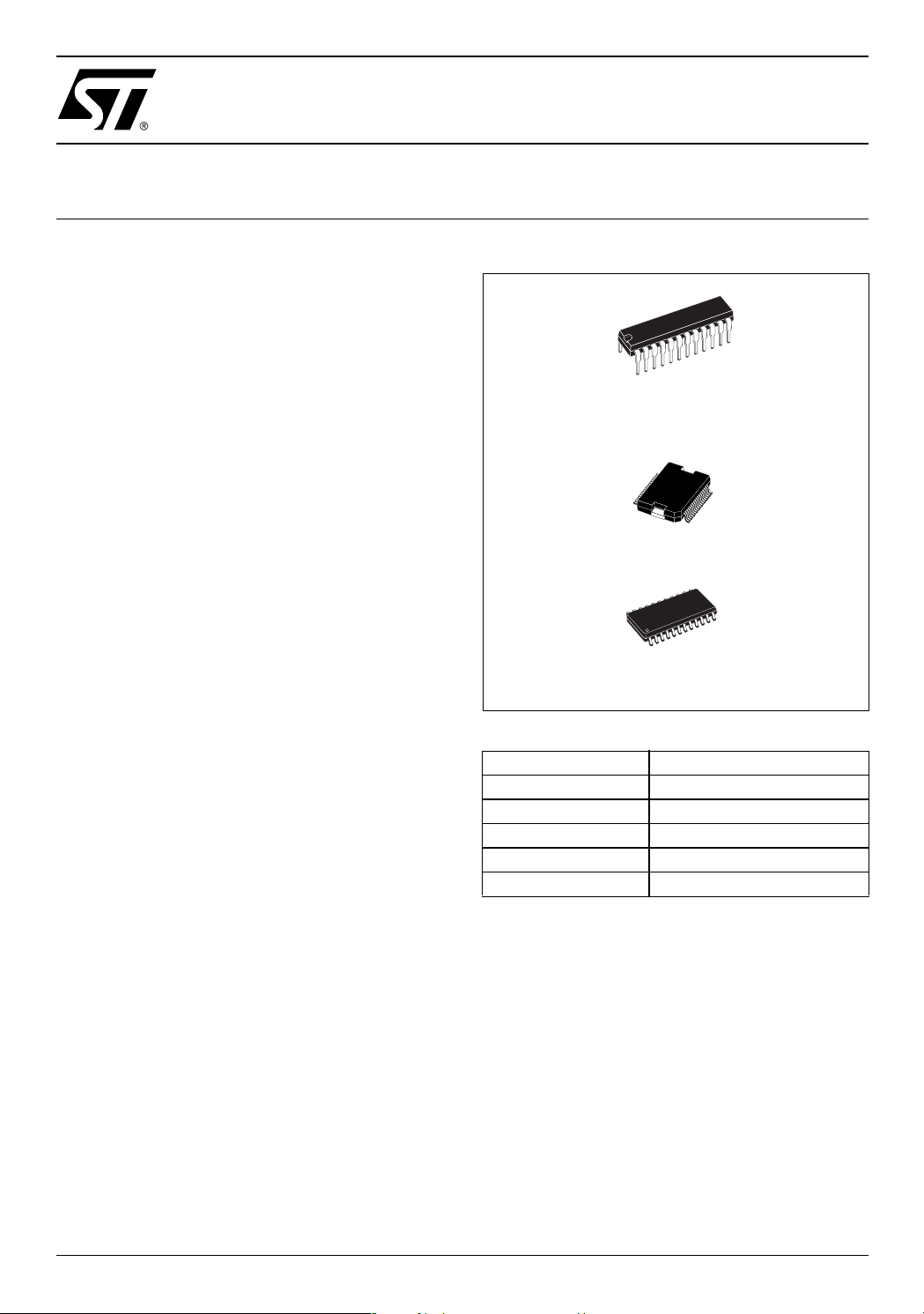
Available in PowerDIP24 (20+2+2), PowerSO36 and
SO24 (20+2+2) packages, the L6229 features a non-
gure 1. Package
PowerDIP24
(20+2+2)
PowerSO36
SO24
(20+2+2)
Table 1. Order Codes
Part Number Package
L6229N PowerDIP24
L6229PD PowerSO36
L6229PDTR PowerSO36 in Tape & Reel
L6229D SO24
L6229DTR SO24 in Tape & Reel
dissipative overcurrent protection on the high side
Power MOSFETs and thermal shutdown.
October 2004
Rev. 3
1/25
L6229
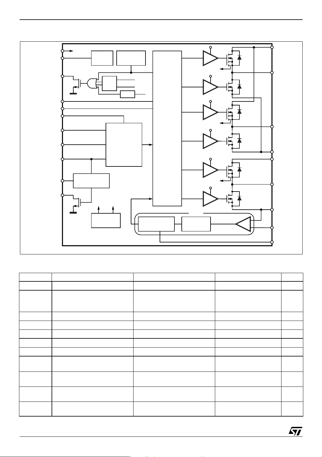
Figure 2. Block Diagram
VBOOT V
VCP
DIAG
EN
BRAKE
FWD/REV
H
3
H
2
H
1
RCPULSE
TACHO
BOOT
CHARGE
PUMP
TACHO
MONOSTABLE
10V
VOLTAGE
REGULATOR
THERMAL
PROTECTION
OCD1
OCD
OCD2
HALL-EFFECT
SENSORS
DECODING
LOGIC
5V
OCD
OCD3
ONE SHOT
MONOSTABLE
GATE
LOGIC
PWM
MASKING
TIME
V
BOOT
OCD1
10V
V
BOOT
OCD2
10V
V
BOOT
OCD3
10V
COMPARATOR
SENSE
VS
A
OUT
1
OUT
2
SENSE
A
VS
B
OUT
3
SENSE
B
+
-
VREF
RCOFF
D99IN1095B
Table 2. Absolute Maximum Ratings
Symbol Parameter Test conditions Value Unit
V
V
V
RCPULSE
V
I
T
2/25
V
V
OD
V
BOOT
, V
IN
V
REF
RCOFF
SENSE
S(peak)
I
S
, T
stg
Supply Voltage VSA = VSB = V
S
Differential Voltage between:
VS
, OUT1, OUT2, SENSEA
A
and VS
, OUT3, SENSE
B
B
VSA = VSB = VS = 60V;
V
SENSEA
Bootstrap Peak Voltage VSA = VSB = V
Logic Inputs Voltage Range -0.3 to 7 V
EN
= V
S
SENSEB
S
= GND
60 V
60 V
VS + 10 V
Voltage Range at pin VREF -0.3 to 7 V
Voltage Range at pin RCOFF -0.3 to 7 V
Voltage Range at pin RCPULSE -0.3 to 7 V
Voltage Range at pins SENSEA
and SENSE
B
Pulsed Supply Current (for each
VS
and VSB pin)
A
DC Supply Current (for each
VS
and VSB pin)
A
Storage and Operating
OP
= VSB = VS; T
V
SA
= VSB = V
V
SA
S
< 1ms 3.55 A
PULSE
-1 to 4 V
1.4 A
-40 to 150 °C
Temperature Range

Table 3. Recommended Operating Condition
Symbol Parameter Test Conditions MIN MAX Unit
L6229
V
V
V
SENSE
I
OUT
f
V
OD
REF
T
SW
Supply Voltage VSA = VSB = V
S
Differential Voltage between:
VS
, OUT1, OUT2, SENSEA and
A
, OUT3, SENSE
VS
B
VSA = VSB = VS;
V
SENSEA
B
= V
S
SENSEB
Voltage Range at pin VREF -0.1 5 V
Voltage Range at pins SENSEA
and SENSE
B
DC Output Current VSA = VSB = V
Operating Junction Temperature -25 125 °C
J
(pulsed tW < trr)
(DC)
S
Switching Frequency 100 KHz
Table 4. Thermal Data
Symbol Description PDIP24 SO24
R
th(j-pins)
R
th(j-case)
R
th(j-amb)1
Maximum Thermal Resistance Junction-Pins 19 15 °C/W
Maximum Thermal Resistance Junction-Case 2 °C/W
MaximumThermal Resistance Junction-Ambient
(1)
44 55 - °C/W
12 52 V
52 V
-6
-1
6
1
1.4 A
PowerSO36
Unit
V
V
(3)
(2)
(4)
--36°C/W
--16°C/W
59 78 63 °C/W
R
th(j-amb)1
R
th(j-amb)1
R
th(j-amb)2
(1) Mounted on a multi-layer FR4 PCB with a dissipating copper surface on the bottom side of 6 cm2 (with a thickness of 35 µm).
(2) Mounted on a multi-layer FR4 PCB with a dissipating copper surface on the top side of 6 cm2 (with a thickness of 35 µm).
(3) Mounted on a multi-layer FR4 PCB with a dissipating copper surface on the top side of 6 cm2 (with a thickness of 35 µm),
(4) Mounted on a multi-layer FR4 PCB without any heat-sinking surface on the board.
Maximum Thermal Resistance Junction-Ambient
MaximumThermal Resistance Junction-Ambient
Maximum Thermal Resistance Junction-Ambient
16 via holes and a ground layer.
3/25
L6229
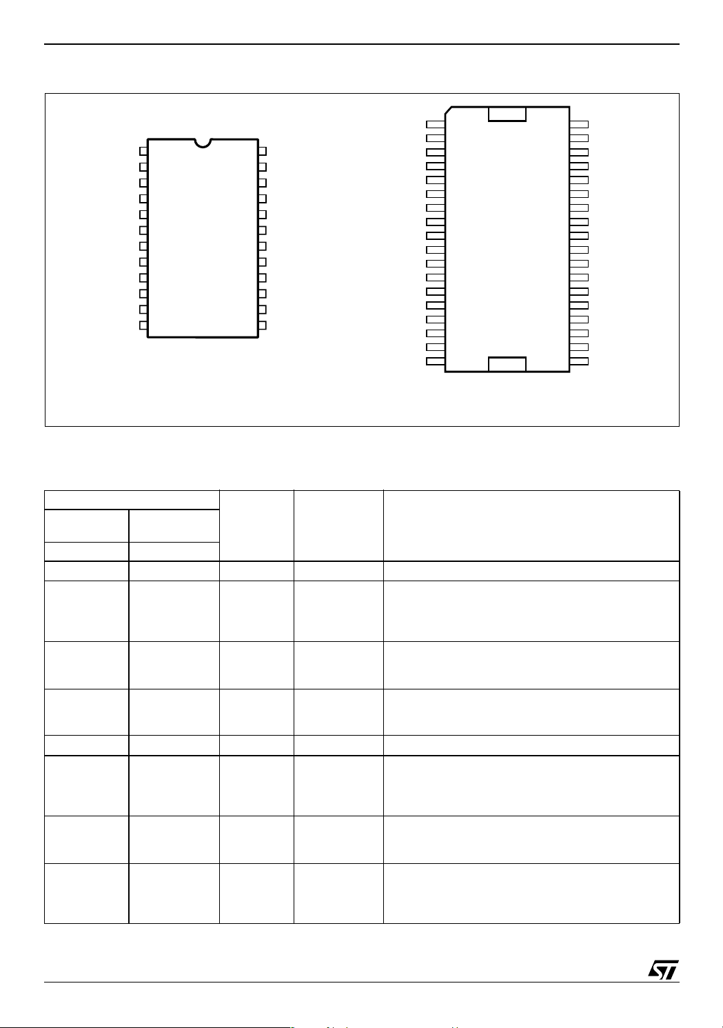
Figure 3. Pin Connections (Top view)
DIAG
SENSE
RCOFF
OUT
GND
GND
TACHO
RCPULSE
SENSE
FWD/REV
EN
1
H
1
2
3
A
4
5
1
6
7
8
9
10
B
11
12
PowerDIP24/SO24
D01IN1194A
GND
N.C.
24
H
3
23
H
2
22
VCP
21
OUT
2
VS
20
18
17
16
15
14
13
A
GND19
GND
VS
B
OUT
3
VBOOT
BRAKE
VREF
N.C.
VS
OUT
N.C.
VCP
DIAG
SENSE
RCOFF
N.C.
OUT
N.C.
N.C.
GND
1
2
3
4
A
5
2
7
H
8
2
H
3
H
10
1
11
12
A
13
14
15
1
16
17
18
D01IN1195A
PowerSO36
36
35
34
33
32
31
30
29
28
27
26
25
24
23
22
21
20
19
(5)
(5) The slug is internally connected to pins 1, 18, 19 and 36 (GND pins).
Table 5. Pin Description
PACKAGE
SO24/
PowerDIP24
PowerSO36
PIN # PIN #
110H
2 11 DIAG Open Drain
3 12 SENSE
4 13 RCOFF RC Pin RC Network Pin. A parallel RC network connected
515OUT
6, 7,
18, 19
1, 18,
19, 36
8 22 TACHO Open Drain
9 24 RCPULSE RC Pin RC Network Pin. A parallel RC network connected
Name Type Function
1
Sensor Input Single Ended Hall Effect Sensor Input 1.
Overcurrent Detection and Thermal Protection pin. An
Output
internal open drain transistor pulls to GND when an
overcurrent on one of the High Side MOSFETs is
detected or during Thermal Protection.
Power Supply Half Bridge 1 and Half Bridge 2 Source Pin. This pin
A
must be connected together with pin SENSE
Power Ground through a sensing power resistor.
between this pin and ground sets the Current
Controller OFF-Time.
Power Output Output 1
1
GND GND Ground terminals. On PowerDIP24 and SO24
packages, these pins are also used for heat
dissipation toward the PCB. On PowerSO36 package
the slug is connected on these pins.
Frequency-to-Voltage open drain output. Every pulse
Output
from pin H
is shaped as a fixed and adjustable length
1
pulse.
between this pin and ground sets the duration of the
Monostable Pulse used for the Frequency-to-Voltage
converter.
GND
N.C.
N.C.
VS
B
OUT
3
N.C.6
VBOOT
BRAKE
VREF9
EN
FWD/REV
SENSE
B
RCPULSE
N.C.
TACHO
N.C.
N.C.
GND
B
to
4/25

Table 5. Pin Description (continued)
PACKAGE
SO24/
PowerDIP24
PowerSO36
PIN # PIN #
10 25 SENSE
11 26 FWD/REV Logic Input Selects the direction of the rotation. HIGH logic level
12 27 EN Logic Input Chip Enable. LOW logic level switches OFF all Power
13 28 VREF Logic Input Current Controller Reference Voltage.
14 29 BRAKE Logic Input Brake Input pin. LOW logic level switches ON all High
15 30 VBOOT Supply Voltage Bootstrap Voltage needed for driving the upper Power
16 32 OUT
17 33 VS
20 4 VS
21 5 OUT
22 7 VCP Output Charge Pump Oscillator Output.
23 8 H
24 9 H
Name Type Function
Power Supply Half Bridge 3 Source Pin. This pin must be connected
B
together with pin SENSE
to Power Ground through a
A
sensing power resistor. At this pin also the Inverting
Input of the Sense Comparator is connected.
sets Forward Operation, whereas LOW logic level sets
Reverse Operation.
If not used, it has to be connected to GND or +5V..
MOSFETs.
If not used, it has to be connected to +5V.
Do not leave this pin open or connect to GND.
Side Power MOSFETs, implementing the Brake
Function.
If not used, it has to be connected to +5V.
MOSFETs.
Power Output Output 3.
3
Power Supply Half Bridge 3 Power Supply Voltage. It must be
B
connected to the supply voltage together with pin VS
Power Supply Half Bridge 1 and Half Bridge 2 Power Supply Voltage.
A
It must be connected to the supply voltage together
with pin VS
Power Output Output 2.
2
2
3
Sensor Input Single Ended Hall Effect Sensor Input 2.
Sensor Input Single Ended Hall Effect Sensor Input 3.
.
B
L6229
A
.
Table 6. Electrical Characteristics
(V
= 48V , T
S
Symbol Parameter Test Conditions Min Typ Max Unit
V
Sth(ON)
V
Sth(OFF)
T
J(OFF)
Turn ON threshold 5.8 6.3 6.8 V
Turn OFF threshold 5 5.5 6 V
Quiescent Supply Current All Bridges OFF;
I
S
Thermal Shutdown Temperature 165 °C
Output DMOS Transistors
R
DS(ON)
High-Side + Low-Side Switch ON
Resistance
I
Leakage Current EN = Low; OUT = V
DSS
= 25 °C , unless otherwise specified)
amb
Tj = -25 to 125°C
Tj = 25 °C 1.47 1.69 Ω
T
=125 °C
j
EN = Low; OUT = GND -0.3 mA
(7)
(6)
CC
510mA
2.35 2.70 Ω
2mA
5/25

L6229
Table 6. Electrical Characteristics (continued)
(V
= 48V , T
S
Symbol Parameter Test Conditions Min Typ Max Unit
Source Drain Diodes
V
Forward ON Voltage ISD = 1.4A, EN = LOW 1.15 1.3 V
SD
t
Reverse Recovery Time If = 1.4A 300 ns
rr
t
Forward Recovery Time 200 ns
fr
Logic Input (H1, H2, H3, EN, FWD/REV, BRAKE)
Low level logic input voltage -0.3 0.8 V
V
IL
V
High level logic input voltage 2 7 V
IH
I
Low level logic input current GND Logic Input Voltage -10 µA
IL
High level logic input current 7V Logic Input Voltage 10 µA
I
IH
V
th(ON)
V
th(OFF)
V
thHYS
Turn-ON Input Threshold 1.8 2.0 V
Turn-OFF Input Threshold 0.8 1.3 V
Input Thresholds Hysteresys 0.25 0.5 V
Switching Characteristics
t
D(on)EN
t
D(off)EN
t
D(on)IN
Enable to out turn-ON delay time
Enable to out turn-OFF delay time
Other Logic Inputs to Output TurnON delay Time
t
D(off)IN
Other Logic Inputs to out Turn-OFF
delay Time
t
RISE
t
FAL L
Output Rise Time
Output Fall Time
Dead Time 0.5 1 µs
t
DT
Charge Pump Frequency
f
CP
PWM Comparator and Monostable
I
RCOFF
V
OFFSET
Source current at pin RC
Offset Voltage on Sense
Comparator
t
prop
Turn OFF Propagation delay
t
blank
Internal Blanking Time on Sense
Comparator
t
ON(min)
t
I
BIAS
Minimum on Time
PWM RecirculationTime R
OFF
Input Bias Current at pin VREF 10 µA
Tacho Monostable
I
RCPULSE
Source Current at pin RCPULSE V
= 25 °C , unless otherwise specified)
amb
(7)
I
LOAD
(7
)
I
LOAD
I
LOAD
I
LOAD
(7)
(7)
I
LOAD
I
LOAD
Tj = -25 to 125°C
V
OFF
(8)
RCOFF
V
ref
V
ref
OFF
R
OFF
RCPULSE
= 1.4 A, Resistive Load 500 650 800 ns
= 1.4 A, Resistive Load 500 1000 ns
= 1.4 A, Resistive Load 1.6 µs
= 1.4 A, Resistive Load 800 ns
= 1.4 A, Resistive Load 40 250 ns
= 1.4 A, Resistive Load 40 250 ns
(6)
0.6 1 MHz
= 2.5 V 3.5 5.5 mA
= 0.5 V ±5 mV
= 0.5 V 500 ns
1µs
2.5 3 µs
= 20kΩ ; C
= 100kΩ ; C
OFF
OFF
=1nF
=1nF
13
61
= 2.5V 3.5 5.5 mA
µs
µs
6/25
L6229
Table 6. Electrical Characteristics (continued)
(V
= 48V , T
S
Symbol Parameter Test Conditions Min Typ Max Unit
t
PULSE
R
TACHO
Monostable of Time R
Open Drain ON Resistance 40 60 Ω
Over Current Detection & Protection
I
SOVER
Supply Overcurrent Protection
Threshold
R
OPDR
t
OCD(ON)
t
OCD(OFF)
(6) Tested at 25°C in a restricted range and guaranteed by characterization.
(7) See Fig. 4.
(8) Measured applying a voltage of 1V to pin SENSE and a voltage drop from 2V to 0V to pin VREF.
(9) See Fig. 5.
Open Drain ON Resistance I
OCD high level leakage current V
I
OH
OCD Turn-ON Delay Time
OCD Turn-OFF Delay Time
Figure 4. Switching Characteristic Definition
= 25 °C , unless otherwise specified)
amb
PUL
R
PUL
= -25 to 125°C
T
J
DIAG
DIAG
(9)
(9)
I
DIAG
I
DIAG
= 20kΩ ; C
= 100kΩ ; C
PUL
PUL
(6)
=1nF
=1nF
12
60
2 2.8 3.55 A
= 4mA 40 60 Ω
= 5V 1 µA
= 4mA; C
= 4mA; C
< 100pF 200 ns
DIAG
< 100pF 100 ns
DIAG
µs
µs
EN
V
th(ON)
V
th(OFF)
I
OUT
90%
10%
D01IN1316
t
D(OFF)EN
Figure 5. Overcurrent Detection Timing Definition
I
OUT
I
SOVER
ON
BRIDGE
OFF
V
DIAG
90%
t
FALL
t
D(ON)EN
t
RISE
t
t
10%
t
OCD(ON)
t
OCD(OFF)
D02IN1387
7/25
L6229
3 CIRCUIT DESCRIPTION
3.1 POWER STAGES and CHARGE PUMP
The L6229 integrates a Three-Phase Bridge, which consists of 6 Power MOSFETs connected as shown on the
Block Diagram. Each Power MOS has an R
diode. Switching patterns are generated by the PWM Current Controller and the Hall Effect Sensor Decoding
Logic (see relative paragraphs). Cross conduction protection is implemented by using a dead time (t
typical value) set by internal timing circuit between the turn off and turn on of two Power MOSFETs in one leg
of a bridge.
Pins VS
and VSB MUST be connected together to the supply voltage (VS).
A
Using N-Channel Power MOS for the upper transistors in the bridge requires a gate drive voltage above the
power supply voltage. The Bootstrapped Supply (V
ternal components to realize a charge pump circuit as shown in Figure 6. The oscillator output (pin VCP) is a
square wave at 600KHz (typically) with 10V amplitude. Recommended values/part numbers for the charge
pump circuit are shown in Table 7.
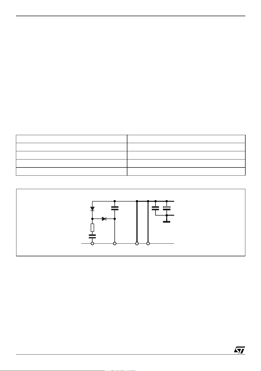
Table 7. Charge Pump External Component Values.
C
BOOT
C
P
R
P
D
1
D
2
= 0.73Ω (typical value @25°C) with intrinsic fast freewheeling
DS(ON)
) is obtained through an internal oscillator and few ex-
BOOT
220nF
10nF
100Ω
1N4148
1N4148
DT
= 1µs
Figure 6. Charge Pump Circuit
V
S
D1
D2
R
P
C
P
VCP VBOOT VS
C
BOOT
VS
B
D01IN1328
A
3.2 LOGIC INPUTS
Pins FWD/REV, BRAKE, EN, H1, H2 and H3 are TTL/CMOS and µC compatible logic inputs. The internal structure is shown in Figure 4. Typical value for turn-ON and turn-OFF thresholds are respectively V
th(OFF)
= 1.3V.
V
th(ON)
= 1.8V and
Pin EN (enable) may be used to implement Overcurrent and Thermal protection by connecting it to the open collector
DIAG output If the protection and an external disable function are both desired, the appropriate connection must be
implemented. When the external signal is from an open collector output, the circuit in Figure 8 can be used . For external circuits that are push pull outputs the circuit in Figure 9 could be used. The resistor R
Ω
the range from 2.2K
to 180KΩ. Recommended values for REN and CEN are respectively 100KΩ and 5.6nF. More
should be chosen in
EN
information for selecting the values can be found in the Overcurrent Protection section.
8/25
 Loading...