ST L6227 User Manual

DMOS DUAL FULL BRIDGE DRIVER
WITH PWM CURRENT CONTROLLER
■
OPERATING SUPPLY VOLTAGE FROM 8 TO 52V
■ 2.8A OUTPUT PEAK CURRENT (1.4A DC)
■ R
■ OPERATING FREQUENCY UP TO 100KHz
■ NON DISSIPATIVE OVERCURRENT
PROTECTION
■ DUAL INDEPENDENT CONSTANT t
CURRENT CONTROLLERS
■ SLOW DECAY SYNCHRONOUS
RECTIFICATION
■ CROSS CONDUCTION PROTECTION
■ THERMAL SHUTDOWN
■ UNDER VOLTAGE LOCKOUT
■
INTEGRATED FAST FREE WHEELING DIODES
TYPICAL APPLICATIONS
■ BIPOLAR STEPPER MOTOR
■ DUAL DC MOTOR
DESCRIPTION
The L6227 is a DMOS Dual Full Bridge designed for
motor control applications, realized in MultiPower-
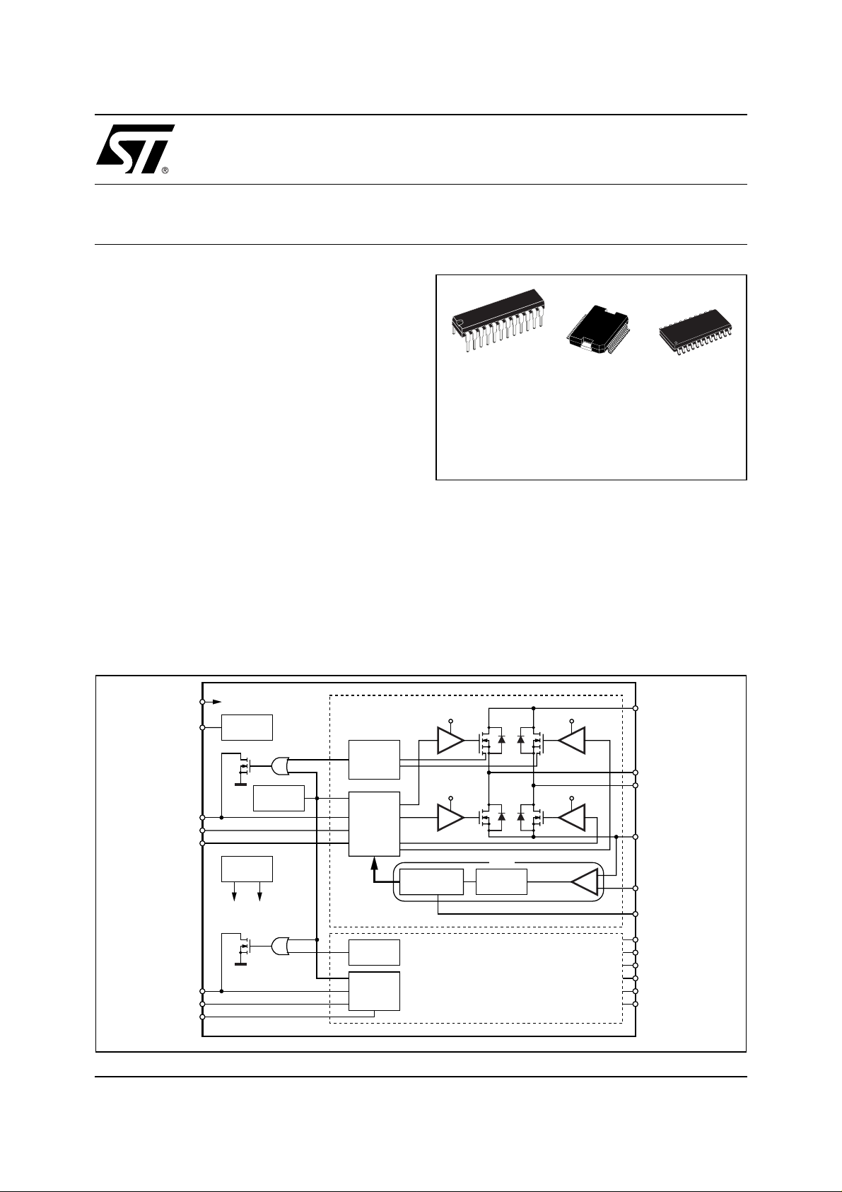
BLOCK DIAGRAM
0.73Ω TYP. VALUE @ Tj = 25 °C
DS(ON)
OFF
PWM
L6227
PowerDIP24
(20+2+2)
BCD technology, which combines isolated DMOS
Power Transistors with CMOS and bipolar c ir cuits on
the same chip. The device also includes two independent constant off time PWM Current Controllers
that performs the chopping regulation. Available in
PowerDIP24 (20+2+2), PowerSO36 and SO24
(20+2+2) packages, the L6227 features a non-dissipative overcurrent protection on the high side Power
MOSFETs and thermal shutdown.
PowerSO36
ORDERING NUMBERS:
L6227N (PowerDIP24)
L6227PD (PowerSO36)
L6227D (SO24)
SO24
(20+2+2)
VBOOT
September 2003
VCP
EN
IN1
IN2
EN
IN1
IN2
V
BOOT
CHARGE
PUMP
OCD
A
THERMAL
PROTECTION
A
A
A
VOLTAGE
REGULATOR
5V10V
OCD
B
B
B
B
OVER
CURRENT
DETECTION
GATE
LOGIC
OVER
CURRENT
DETECTION
GATE
LOGIC
V
BOOT
10V 10V
ONE SHOT
MONOSTABLE
MASKING
PWM
TIME
V
BOOT
SENSE
COMPARATOR
BRIDGE A
BRIDGE B
+
-
D99IN1085A
VS
A
OUT1
OUT2
SENSE
VREF
RC
A
V
S
B
OUT1
OUT2
SENSE
VREF
RC
B
A
A
A
A
B
B
B
B
1/22

L6227
ABSOLUTE MAXIMUM RATINGS
Symbol Parameter Test conditions Value Unit
V
S
V
OD
V
BOOT
V
IN,VEN
V
REFA
V
REFB
V
RCA, VRCB
V
SENSEA,
V
SENSEB
I
S(peak)
I
S
, T
T
stg
Supply Voltage
Differential Voltage between
VSA, OUT1A, OUT2A, SENSEA and
VSB, OUT1B, OUT2B, SENSE
Bootstrap Peak Voltage
VSA =
VSB = V
VSA =
VSB = VS = 60V;
V
SENSEA
B
VSA =
VSB = V
= V
S
SENSEB
S
= GND
60 V
60 V
VS + 10 V
Input and Enable Voltage Range -0.3 to +7 V
,
Voltage Range at pins V
and V
REFB
REFA
Voltage Range at pins RCA and
RC
B
Voltage Range at pins SENSEA
and SENSE
B
Pulsed Supply Current (for each
pin), internally limited by the
V
S
VSA =
t
PULSE
VSB = VS;
< 1ms
-0.3 to +7 V
-0.3 to +7 V
-1 to +4 V
3.55 A
overcurrent protection
RMS Supply Current (for each
pin)
V
S
Storage and Operating
OP
VSA =
VSB = V
S
1.4 A
-40 to 150 °C
Temperature Range
RECOMMENDED OPERATING CONDITIONS
Symbol Parameter Test Conditions MIN MAX Unit
V
S
V
OD
,
V
REFA
V
REFB
V
SENSEA,
V
SENSEB
I
OUT
T
j
f
sw
Supply Voltage
Differential Voltage Between
VSA, OUT1A, OUT2A, SENSEA and
VSB, OUT1B, OUT2B, SENSE
Voltage Range at pins V
and V
REFB
REFA
Voltage Range at pins SENSEA
and SENSE
B
RMS Output Current 1.4 A
Operating Junction Temperature -25 +125 °C
Switching Frequency 100 KHz
VSA =
VSA =
V
SENSEA
B
(pulsed tW < trr)
(DC)
VSB = V
VSB = VS;
= V
SENSEB
S
852V
52 V
-0.1 5 V
-6
-1
6
1
V
V
2/22

L6227
THERMA L D ATA
Symbol Description PowerDIP24 SO24 PowerSO36 Unit
R
th-j-pins
R
th-j-case
R
th-j-amb1
R
th-j-amb1
R
th-j-amb1
R
th-j-amb2
(1) Mounted on a multi-layer FR4 PCB with a dissipati ng copper surface on the bottom side of 6cm2 (with a thickness of 35µm).
(2) Mounted on a multi-layer FR4 PCB with a dissipati ng copper surface on the top side of 6cm2 (with a thic kness of 35µm ).
(3) Mounted on a multi-layer FR4 PCB with a dissipating copper surface on the top side of 6cm2 (with a thickness of 35µm), 16 via holes
and a groun d l ayer.
(4) Mounted on a multi-layer FR4 PCB without any hea t s i nking surfac e on the board.
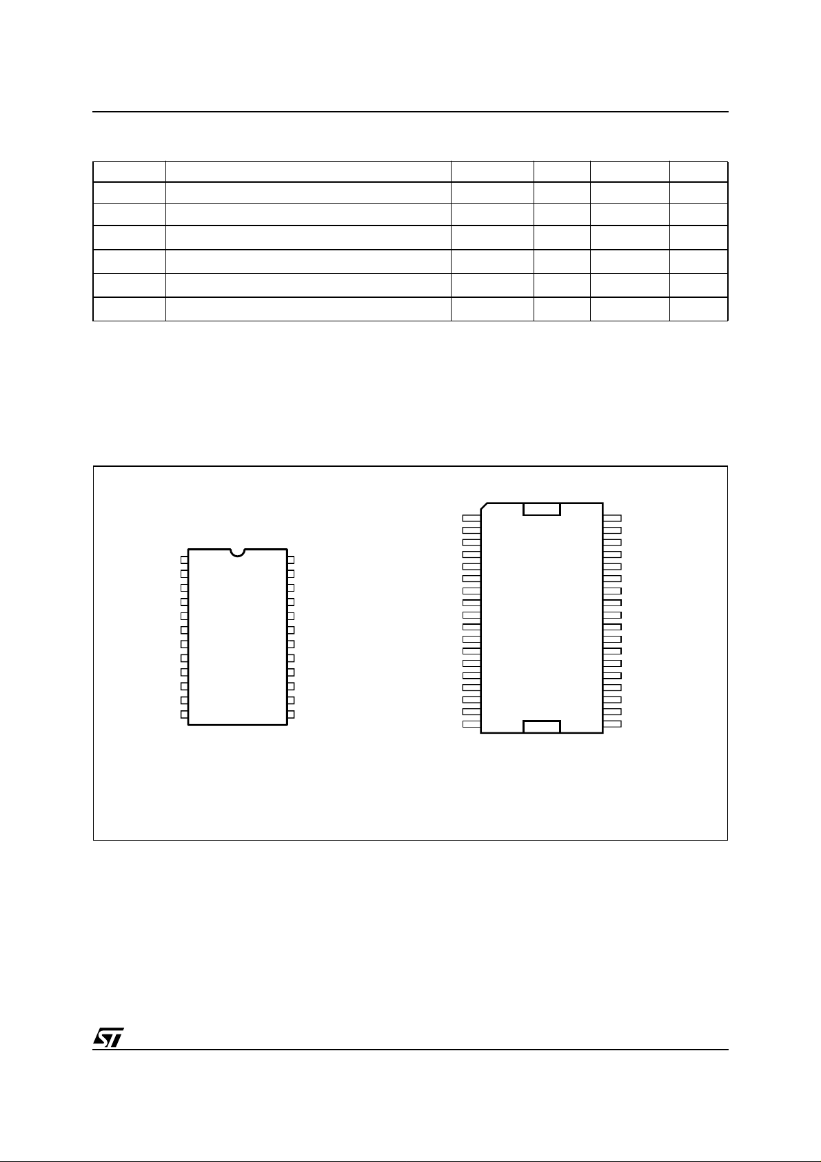
PIN CONNECTIONS (Top View)
Maximum Thermal Resistance Junction-Pins 19 15 - °C/W
Maximum Thermal Resistance Junction-Case - - 2 °C/W
Maximum Thermal Resistance Junction-Ambient
Maximum Thermal Resistance Junction-Ambient
Maximum Thermal Resistance Junction-Ambient
Maximum Thermal Resistance Junction-Ambient
1
2
3
4
44 52 - °C/W
--36°C/W
--16°C/W
59 78 63 °C/W
IN1
IN2
SENSE
RC
OUT1
GND
GND
OUT1
RC
SENSE
IN1
IN2
1
A
2
A
3
A
4
A
5
A
6
7
8
B
9
B
10
B
11
B
12
B
D02IN1346
VREF
24
23
22
21
20
EN
VCP
OUT2
VS
A
A
A
A
GND19
GND
18
VS
17
B
OUT2
16
15
14
13
VBOOT
EN
B
VREF
B
B
PowerDIP24/SO24
(5) The slug is internally connected to pins 1,18,19 and 36 (GND pins).
GND
N.C.
N.C.
VS
OUT2
N.C. N.C.
VCP
EN
VREF
IN1
IN2
SENSE
RC
N.C.
OUT1
N.C.
N.C. N.C.
GND GND
1
2
3
4
A
5
A
6
7
8
A
9
A
10 27
A
11
A
12
A
13 24
A
14
15
A
16
17
18
D02IN1347
PowerSO36
36
35
34
33
32
31
30
29
28
26
25
23
22
21
20
19
(5)
GND
N.C.
N.C.
VS
B
OUT2
VBOOT
EN
B
VREF
IN2
B
IN1
B
SENSE
RC
B
N.C.
OUT1
N.C.
B
B
B
B
3/22

L6227
PIN DESCRIPTION
PACKA GE
SO24/
PowerDIP24
PowerSO36
Name Type Function
PIN # PIN #
1 10 IN1
2 11 IN2
3 12 SENSE
413RC
5 15 OUT1
6, 7,
18, 19
1, 18,
19, 36
GND GND Signal Ground terminals. In Power DIP and SO packages,
8 22 OUT1
924RC
10 25 SENSE
11 26 IN1
12 27 IN2
13 28 VREF
14 29 EN
A
A
Logic input Bridge A Logic Input 1.
Logic input Bridge A Logic Input 2.
Power Supply Bridge A Source Pin. This pin must be connected to Power
A
Ground through a sensing power resistor.
A
RC Pin RC Network Pin. A parallel RC network connected
between this pin and ground sets the Current Controller
OFF-Time of the Bridge A.
Power Output Bridge A Output 1.
A
these pins are also used for heat dissipation toward the
PCB.
Power Output Bridge B Output 1.
B
B
RC Pin RC Network Pin. A parallel RC network connected
between this pin and ground sets the Current Controller
OFF-Time of the Bridge B.
Power Supply Bridge B Source Pin. This pin must be connected to Power
B
Ground through a sensing power resistor.
B
B
Logic Input Bridge B Input 1
Logic Input Bridge B Input 2
Analog Input Bridge B Current Controller Reference Voltage.
B
Do not leave this pin open or connect to GND.
Logic Input (6) Bridge B Enable. LOW logic level switches OFF all Power
B
MOSFETs of Bridge B. This pin is also connected to the
collector of the Overcurrent and Thermal Protection
transistor to implement over current protection.
If not used, it has to be connected to +5V through a
resistor.
15 30 VBOOT Supply
Voltage
16 32 OUT2
17 33 VS
Power Output Bridge B Output 2.
B
Power Supply Bridge B Power Supply Voltage. It must be connected to
B
Bootstrap Voltage needed for driving the upper Power
MOSFETs of both Bridge A and Bridge B.
the supply voltage together with pin VS
20 4 VS
Power Supply Bridge A Power Supply Voltage. It must be connected to
A
the supply voltage together with pin VS
21 5 OUT2
Power Output Bridge A Output 2.
A
22 7 VCP Output Charge Pump Oscillator Output.
4/22
.
A
.
B

L6227
PIN DESCRIPTION
23 8 EN
(continued)
Logic Input (6) Bridge A Enable. LOW logic level switches OFF all Power
A
MOSFETs of Bridge A. This pin is also connected to the
collector of the Overcurrent and Thermal Protection
transistor to implement over current protection.
If not used, it has to be connected to +5V through a
resistor.
24 9 VREF
Analog Input Bridge A Current Controller Reference Voltage.
A
Do not leave this pin open or connect to GND.
(6) Also connected a t t he output drain of the Over cu rrent and Thermal protection M OSFET. Therefore, i t has to be driven pu tti n g in
series a re si stor with a v al ue in the ran ge of 2.2KΩ - 180KΩ, recomme nded 100KΩ.
ELECTRICAL CHARACTERISTICS
(T
= 25 °C, Vs = 48V, unless otherwise specified)
amb
Symbol Parameter Test Conditions Min Typ Max Unit
V
Sth(ON)
V
Sth(OFF)
T
j(OFF)
Output DMOS Transistors
Turn-on Threshold 5.8 6.3 6.8 V
Turn-off Threshold 5 5.5 6 V
I
Quiescent Supply Current All Bridges OFF;
S
T
j
= -25°C to 125°C
(7)
510mA
Thermal Shutdown Temperature 165 °C
R
DS(ON)
High-Side +Low-Side Switch ON
Resistance
I
DSS
Leakage Current EN = Low; OUT = V
Source Drain Diodes
V
Forward ON Voltage ISD = 1.4A, EN = LOW 1.15 1.3 V
SD
t
Reverse Recovery Time If = 1.4A 300 ns
rr
t
Forward Recovery Time 200 ns
fr
Logic Input
V
V
V
th(ON)
V
th(OFF)
V
th(HYS)
Low level logic input voltage -0.3 0.8 V
IL
High level logic input voltage 2 7 V
IH
I
Low Level Logic Input Current GND Logic Input Voltage -10 µA
IL
I
High Level Logic Input Current 7V Logic Input Voltage 10 µA
IH
Turn-on Input Threshold 1.8 2.0 V
Turn-off Input Threshold 0.8 1.3 V
Input Threshold Hysteresis 0.25 0.5 V
Tj = 25 °C 1.47 1.69 Ω
T
=125 °C
j
(7)
S
2.35 2.7 Ω
2mA
EN = Low; OUT = GND -0.3 mA
Switching Characteristics
t
D(on)EN
Enable to out turn ON delay time
(8)
I
=1.4A, Resistive Load 500 800 ns
LOAD
5/22

L6227
ELECTRICAL CHARACTERISTICS (continued)
(T
= 25 °C, Vs = 48V, unless otherwise specified)
amb
Symbol Parameter Test Conditions Min Typ Max Unit
t
D(on)IN
t
RISE
t
D(off)EN
t
D(off)IN
t
FALL
f
Input to out turn ON delay time
Output rise time
(8)
Enable to out turn OFF delay time
Input to out turn OFF delay time
Output Fall Time
Dead Time Protection 0.5 1 µs
t
dt
CP
Charge pump frequency
(8)
PWM Comparator and Monostable
I
RCA, IRCB
V
offset
Source Current at pins RCA and
RC
B
Offset Voltage on Sense
Comparator
t
PROP
t
BLANK
Turn OFF Propagation Delay
Internal Blanking Time on
SENSE pins
I
=1.4A, Resistive Load
LOAD
1.9 µs
(dead time included)
I
=1.4A, Resistive Load 40 250 ns
LOAD
(8)
I
=1.4A, Resistive Load 500 800 1000 ns
LOAD
I
=1.4A, Resistive Load 500 800 1000 ns
LOAD
I
=1.4A, Resistive Load 40 250 ns
LOAD
-25°C<Tj <125°C 0.6 1 MHz
V
(9)
= V
RCA
V
REFA, VREFB
= 2.5V 3.5 5.5 mA
RCB
= 0.5V ±5 mV
500 ns
1µs
t
ON(MIN)
t
OFF
I
BIAS
Minimum On Time 2.5 3 µs
PWM Recirculation Time R
OFF
R
OFF
= 20KΩ; C
= 100KΩ; C
OFF
OFF
= 1nF
= 1nF
Input Bias Current at pins VREFA
and VREF
B
Over Current Protection
I
SOVER
R
OPDR
t
OCD(ON)
t
OCD(OFF)
(7) Tested at 25°C in a restricted range and guaranteed by characterization.
(8) See Fig. 1.
(9) Measured applying a voltage of 1V to pin SEN S E and a voltag e drop from 2V to 0V to pin VREF.
(10) See Fig. 2.
Input Supply Overcurrent
Protection Threshold
= -25°C to 125°C
T
j
Open Drain ON Resistance I = 4mA 40 60 Ω
OCD Turn-on Delay Time (10) I = 4mA; CEN < 100pF 200 ns
OCD Turn-off Delay Time (10) I = 4mA; CEN < 100pF 100 ns
(7)
2 2.8 3.55 A
13
61
µs
µs
10 µA
6/22

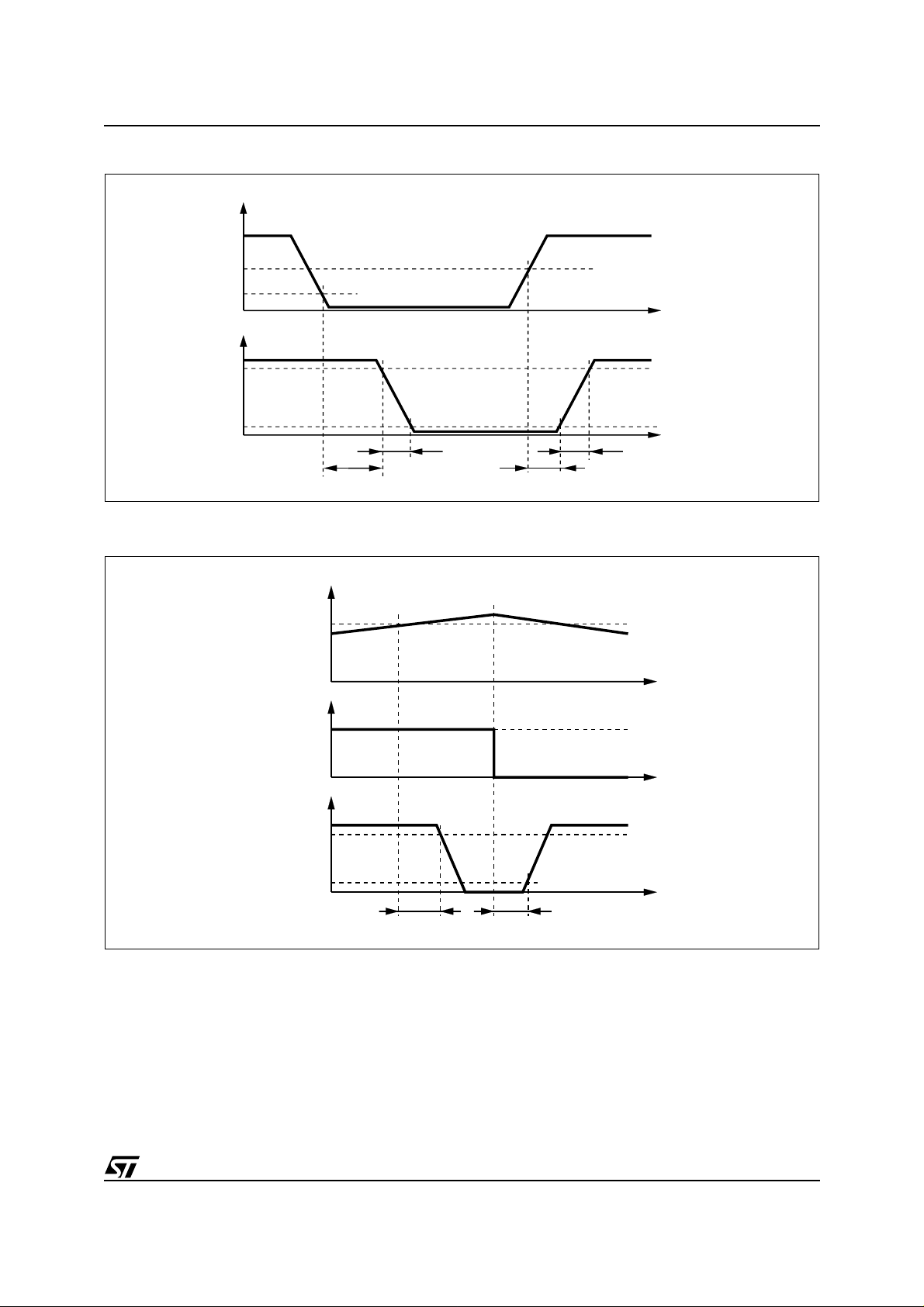
Figure 1. Switching Characteristic Definition
EN
V
th(ON)
V
th(OFF)
I
OUT
90%
10%
D01IN1316
t
D(OFF)EN
t
FALL
Figure 2. Ove rcurrent Detect i on Timi ng Definition
t
D(ON)EN
t
RISE
L6227
t
t
I
OUT
I
SOVER
ON
BRIDGE
OFF
V
EN
90%
10%
t
OCD(ON)
t
OCD(OFF)
D02IN1399
7/22
 Loading...