

Features
■ Operating supply voltage from 8 to 52 V
■ 2.8 A output peak current (1.4 A DC)
■ R
0.73 Ω typ. value @ TJ = 25 °C
DS(on)
■ Operating frequency up to 100 kHz
■ Programmable high side overcurrent detection
and protection
■ Diagnostic output
■ Paralleled operation
■ Cross conduction protection
■ Thermal shutdown
■ Under voltage lockout
■ Integrated fast free wheeling diodes
Applications
■ Bipolar stepper motor
■ Dual or quad DC motor
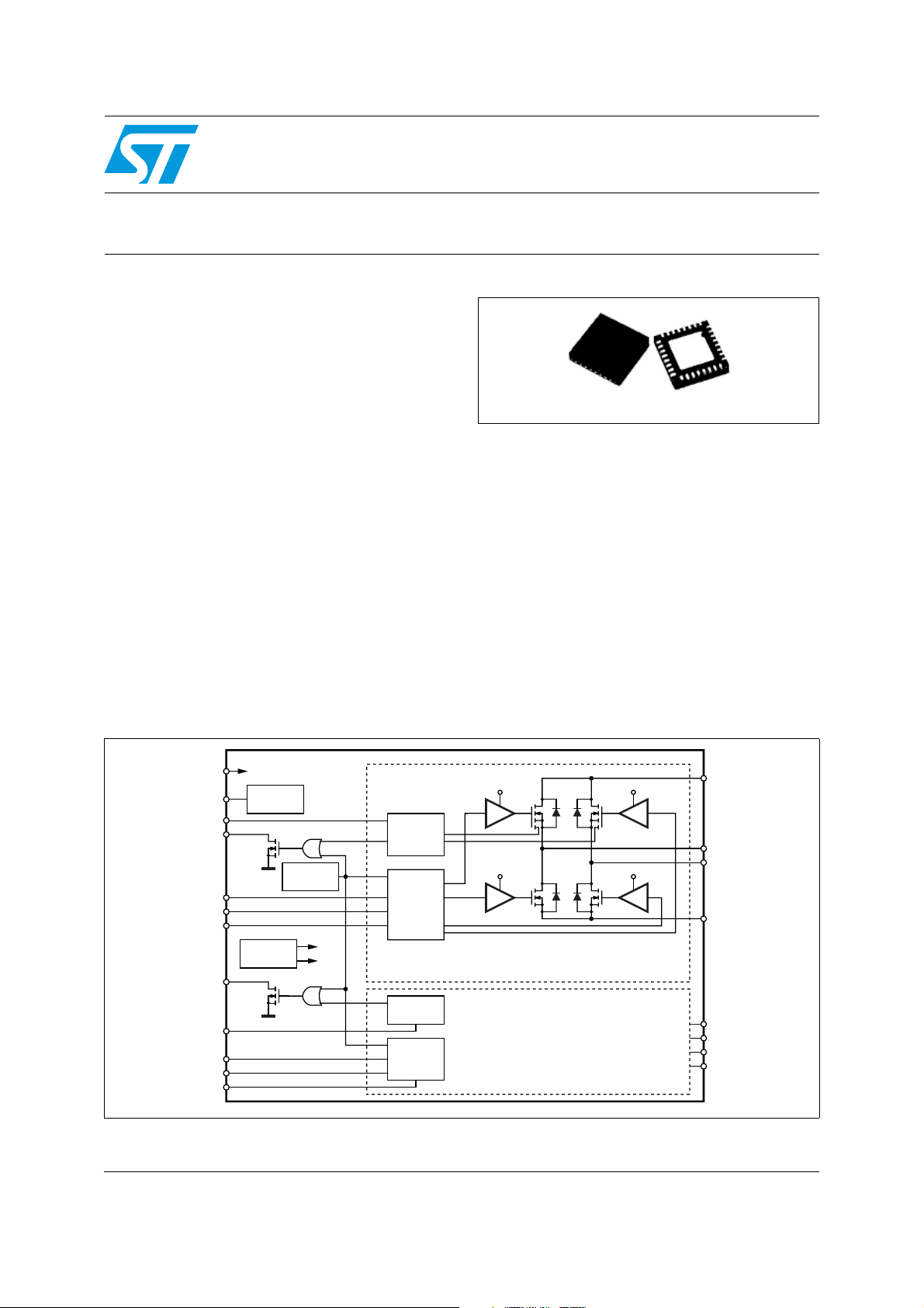
Figure 1. Block diagram
L6226Q
DMOS dual full bridge driver
Description
The L6226Q is a DMOS dual full bridge designed
for motor control applications, realized in
BCDmultipower technology, which combines
isolated DMOS power transistors with CMOS and
bipolar circuits on the same chip. Available in
QFN32 5x5 package, the L6226Q features
thermal shutdown and a non-dissipative
overcurrent detection on the high side power
MOSFETs plus a diagnostic output that can be
easily used to implement the overcurrent
protection.
VBOOT
VCP
PROGCL
OCD
EN
IN1
IN2
OCD
PROGCL
EN
IN1
IN2
A
A
A
A
A
B
B
B
B
B
V
BOOT
CHARGE
PUMP
VOLTAGE
REGULATOR
OCD
THERMAL
PROTECTION
OCD
10V
5V
VS
V
BOOT
OVER
A
B
CURRENT
DETECTION
GATE
LOGIC
OVER
CURRENT
DETECTION
GATE
LOGIC
10V 10V
V
BOOT
BRIDGE A
BRIDGE B
D99IN1088A
A
OUT1
OUT2
SENSE
V
S
B
OUT1
OUT2
SENSE
A
A
A
B
B
B
August 2010 Doc ID 14335 Rev 5 1/29
www.st.com
29

Contents L6226Q
Contents
1 Electrical data . . . . . . . . . . . . . . . . . . . . . . . . . . . . . . . . . . . . . . . . . . . . . . 3
1.1 Absolute maximum ratings . . . . . . . . . . . . . . . . . . . . . . . . . . . . . . . . . . . . . 3
1.2 Recommended operating conditions . . . . . . . . . . . . . . . . . . . . . . . . . . . . . 3
1.3 Thermal data . . . . . . . . . . . . . . . . . . . . . . . . . . . . . . . . . . . . . . . . . . . . . . . 4
2 Pin connection . . . . . . . . . . . . . . . . . . . . . . . . . . . . . . . . . . . . . . . . . . . . . . 5
3 Electrical characteristics . . . . . . . . . . . . . . . . . . . . . . . . . . . . . . . . . . . . . 7
4 Circuit description . . . . . . . . . . . . . . . . . . . . . . . . . . . . . . . . . . . . . . . . . . 10
4.1 Power stages and charge pump . . . . . . . . . . . . . . . . . . . . . . . . . . . . . . . . 10
4.2 Logic inputs . . . . . . . . . . . . . . . . . . . . . . . . . . . . . . . . . . . . . . . . . . . . . . . 11
4.3 Truth table . . . . . . . . . . . . . . . . . . . . . . . . . . . . . . . . . . . . . . . . . . . . . . . . . 12
4.4 Non-dissipative overcurrent detection and protection . . . . . . . . . . . . . . . 12
4.5 Thermal protection . . . . . . . . . . . . . . . . . . . . . . . . . . . . . . . . . . . . . . . . . . 16
5 Application information . . . . . . . . . . . . . . . . . . . . . . . . . . . . . . . . . . . . . 17
6 Paralleled operation . . . . . . . . . . . . . . . . . . . . . . . . . . . . . . . . . . . . . . . . 19
7 Output current capability and IC power dissipation . . . . . . . . . . . . . . 23
8 Thermal management . . . . . . . . . . . . . . . . . . . . . . . . . . . . . . . . . . . . . . . 24
9 Package mechanical data . . . . . . . . . . . . . . . . . . . . . . . . . . . . . . . . . . . . 25
10 Order codes . . . . . . . . . . . . . . . . . . . . . . . . . . . . . . . . . . . . . . . . . . . . . . . 27
11 Revision history . . . . . . . . . . . . . . . . . . . . . . . . . . . . . . . . . . . . . . . . . . . 28
2/29 Doc ID 14335 Rev 5

L6226Q Electrical data
1 Electrical data
1.1 Absolute maximum ratings
Table 1. Absolute maximum ratings
Symbol Parameter Parameter Value Unit
V
S
Supply voltage
Differential voltage between
V
OD
OCD
,OCDBOCD pins voltage range -0.3 to + 10 V
A
PROGCL
PROGCL
V
BOOT
V
IN,VEN
V
SENSEA,
V
SENSEB
VSA, OUT1A, OUT2A, SENSEA and
, OUT1B, OUT2B, SENSE
VS
B
,
A
PROGCL pins voltage range -0.3 to + 7 V
B
B
Bootstrap peak voltage
Input and enable voltage range -0.3 to + 7 V
Voltage range at pins SENSEA and
SENSE
B
Pulsed supply current (for each VS
I
S(peak)
pin), internally limited by the
overcurrent protection
I
S
T
, T
stg
RMS supply current (for each VS pin)
Storage and operating temperature
OP
range
VSA =
VSB = V
VSA =
VSB = VS = 60 V,
V
VSA =
VSA =
t
PULSE
VSA =
SENSEA
VSB = V
VSB = VS,
< 1 ms
VSB = V
= V
S
SENSEB
S
S
1.2 Recommended operating conditions
= GND
60 V
60 V
VS + 10 V
-1 to + 4 V
3.55 A
1.4 A
-40 to 150 °C
Table 2. Recommended operating conditions
Symbol Parameter Parameter Min Max Unit
V
S
V
OD
V
SENSEA,
V
SENSEB
I
OUT
T
J
f
sw
Supply voltage
Differential voltage between
, OUT1A, OUT2A, SENSEA and
VS
A
, OUT1B, OUT2B, SENSE
VS
B
B
Voltage range at pins SENSEA and
SENSE
B
VSA =
VSB = V
VSA =
VSB = VS,
V
SENSEA
= V
SENSEB
(pulsed tW < trr)
(DC)
S
852V
52 V
-6
-1
6
1
RMS output current 1.4 A
Operating junction temperature -25 +125 °C
Switching frequency 100 kHz
Doc ID 14335 Rev 5 3/29
V
V

Electrical data L6226Q
1.3 Thermal data
Table 3. Thermal data
Symbol Parameter Value Unit
R
th(JA)
1. Mounted on a double-layer FR4 PCB with a dissipating copper surface of 0.5 cm2 on the top side plus 6
cm2 ground layer connected through 18 via holes (9 below the IC).
Thermal resistance junction-ambient max.
(1)
42 °C/W
4/29 Doc ID 14335 Rev 5
L6226Q Pin connection
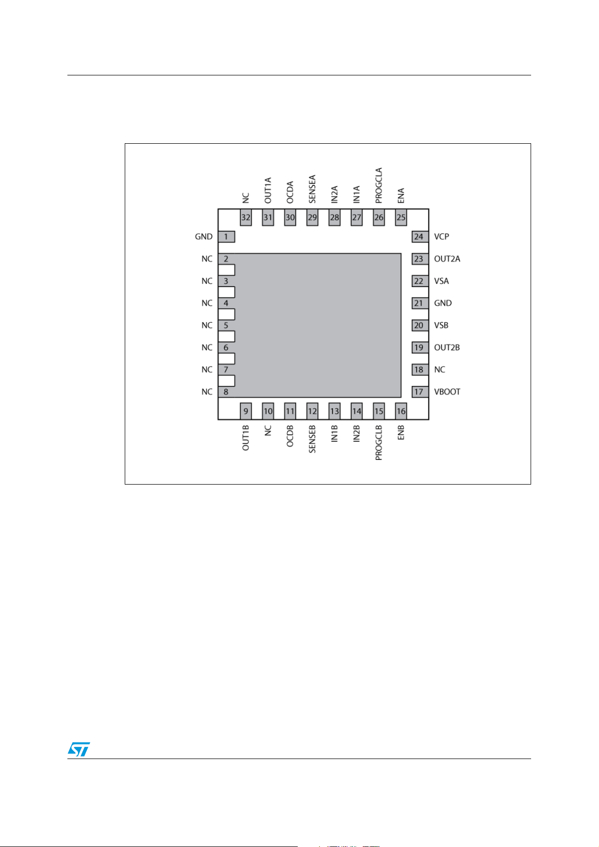
2 Pin connection
Figure 2. Pin connection (top view)
Note: 1 The pins 2 to 8 are connected to die PAD.
2 The die PAD must be connected to GND pin.
Doc ID 14335 Rev 5 5/29

Pin connection L6226Q
Table 4. Pin description
N° Pin Type Function
1, 21 GND GND Signal ground terminals.
9 OUT1B Power output Bridge B output 1.
11 OCDB
12 SENSEB Power supply
13 IN1B Logic input Bridge B input 1
14 IN2B Logic input Bridge B input 2
15 PROGCLB R pin
16 ENB Logic input
17 VBOOT
19 OUT2B Power output Bridge B output 2.
20 VSB Power supply
22 VSA Power supply
Open drain
output
Supply
voltage
Bridge B overcurrent detection and thermal protection pin. An internal open
drain transistor pulls to GND when overcurrent on bridge B is detected or in
case of thermal protection.
Bridge B source pin. This pin must be connected to power ground directly or
through a sensing power resistor.
Bridge B overcurrent level programming. A resistor connected between this
pin and ground sets the programmable current limiting value for the bridge B.
By connecting this pin to ground the maximum current is set. This pin cannot
be left non-connected.
Bridge B enable. LOW logic level switches OFF all power MOSFETs of
bridge B.
If not used, it has to be connected to +5 V.
Bootstrap voltage needed for driving the upper power MOSFETs of both
bridge A and bridge B.
Bridge B power supply voltage. It must be connected to the supply voltage
together with pin VSA.
Bridge A power supply voltage. It must be connected to the supply voltage
together with pin VSB.
23 OUT2A Power output Bridge A output 2.
24 VCP Output Charge pump oscillator output.
Bridge A enable. LOW logic level switches OFF all power MOSFETs of
25 ENA Logic input
26 PROGCLA R pin
27 IN1A Logic input Bridge A logic input 1.
28 IN2A Logic input Bridge A logic input 2.
29 SENSEA Power supply
30 OCDA
31 OUT1A Power output Bridge A output 1.
6/29 Doc ID 14335 Rev 5
Open drain
output
bridge A.
If not used, it has to be connected to +5 V.
Bridge A overcurrent level programming. A resistor connected between this
pin and ground sets the programmable current limiting value for the bridge A.
By connecting this pin to ground the maximum current is set. This pin cannot
be left non-connected.
Bridge A source pin. This pin must be connected to power ground directly or
through a sensing power resistor.
Bridge A overcurrent detection and thermal protection pin. An internal open
drain transistor pulls to GND when overcurrent on bridge A is detected or in
case of thermal protection.

L6226Q Electrical characteristics
3 Electrical characteristics
TA = 25 °C, Vs = 48 V, unless otherwise specified
Table 5. Electrical characteristics
Symbol Parameter Test condition Min Typ Max Unit
V
Sth(ON)
V
Sth(OFF)
I
T
J(OFF)
S
Turn-on threshold 5.8 6.3 6.8 V
Turn-off threshold 5 5.5 6 V
Quiescent supply current
Thermal shutdown temperature 165 °C
Output DMOS transistors
R
DS(on)
I
DSS
High-side + low-side switch ON
resistance
Leakage current
Source drain diodes
V
SD
t
rr
t
fr
Forward ON voltage ISD = 2.8 A, EN = LOW 1.15 1.3 V
Reverse recovery time If = 1.4 A 300 ns
Forward recovery time 200 ns
Logic input
V
V
I
V
th(ON)
V
th(OFF)
V
th(HYS)
IH
I
IL
IH
Low level logic input voltage -0.3 0.8 V
IL
High level logic input voltage 2 7 V
Low level logic input current GND logic input voltage -10 µA
High level logic input current 7 V logic input voltage 10 µA
Turn-on input threshold 1.8 2.0 V
Turn-off input threshold 0.8 1.3 V
Input threshold hysteresis 0.25 0.5 V
Switching characteristics
t
D(on)EN
t
D(on)IN
t
RISE
t
D(off)EN
t
D(off)IN
t
FAL L
Enable to out turn ON delay time
Input to out turn ON delay time
Output rise time
Enable to out turn OFF delay time
Input to out turn OFF delay time I
Output fall time
(2)
(2)
(2)
All bridges OFF;
TJ = -25 °C to 125 °C
= 25 °C 1.47 1.69 Ω
T
J
T
= 125 °C
J
(1)
EN = Low; OUT = V
(1)
S
510mA
2.35 2.70 Ω
EN = Low; OUT = GND -0.3 mA
I
=1.4 A, resistive load 500 800 ns
LOAD
I
=1.4 A, resistive load
LOAD
(dead time included)
I
LOAD
(2)
I
LOAD
LOAD
I
LOAD
=1.4 A, resistive load 40 250 ns
=1.4 A, resistive load 500 800 1000 ns
=1.4 A, resistive load 500 800 1000 ns
=1.4 A, resistive load 40 250 ns
1.9 µs
2mA
Doc ID 14335 Rev 5 7/29
Electrical characteristics L6226Q
Table 5. Electrical characteristics (continued)
Symbol Parameter Test condition Min Typ Max Unit
t
dt
f
CP
Dead time protection 0.5 1 µs
Charge pump frequency
-25 °C < TJ < 125 °C 0.6 1 MHz
Over current detection
I
s over
R
OPDR
t
OCD(ON)
t
OCD(OFF)
1. Tested at 25 °C in a restricted range and guaranteed by characterization.
2. See Figure 3
3. See Figure 4
Input supply over current detection
threshold
Open drain ON resistance I = 4 mA 40 60 Ω
OCD turn-on delay time
OCD turn-off delay time
(3)
(3)
-25 °C<T
-25 °C<T
-25 °C<TJ<125 °C;RCL= GND
I = 4 mA; CEN < 100 pF 200 ns
I = 4 mA; CEN < 100 pF 100 ns
<125 °C;RCL=39 kΩ
J
<125 °C;RCL= 5 kΩ
J
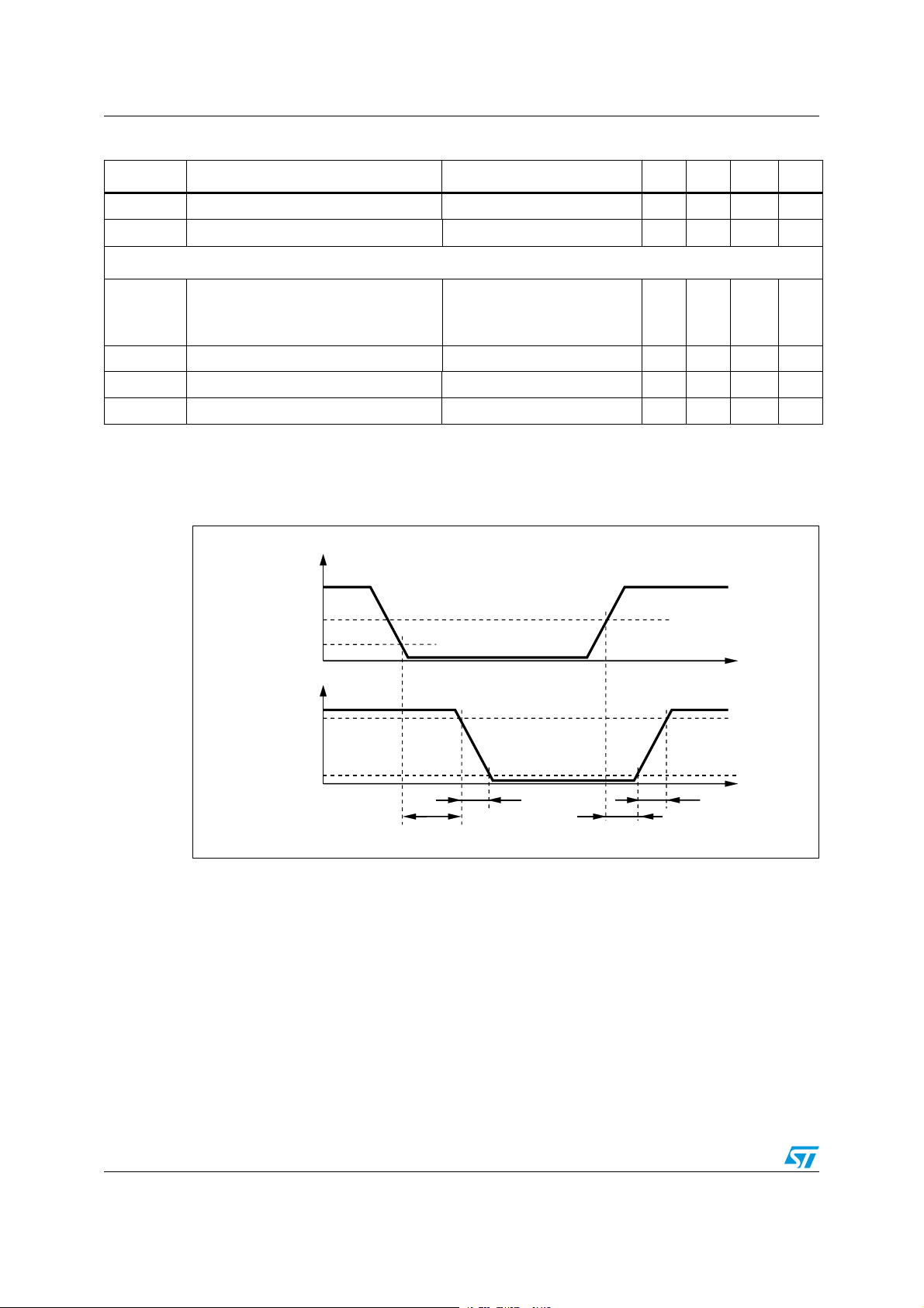
Figure 3. Switching characteristic definition
(1
9
WK21
9
WK2))
,
287
-10%
-10%
-30%
0.29
2.21
2.8
+10%
+10%
+30%
W
A
A
A
',1
W
'2))(1
W
)$//
8/29 Doc ID 14335 Rev 5
W
'21(1
W
5,6(
W
L6226Q Electrical characteristics
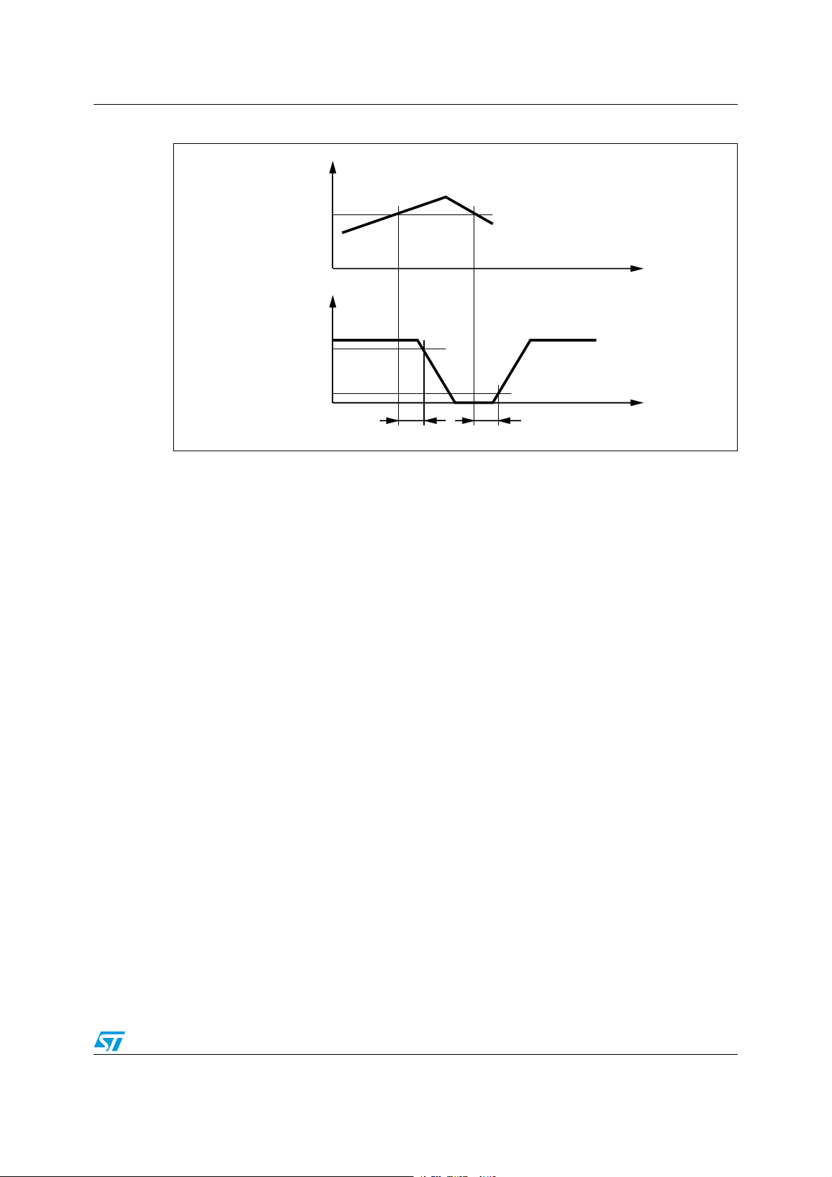
Figure 4. Overcurrent detection timing definition
,
287
2&'
7KUHVKROG
W
9
2&'
W
W
2&'21
W
2&'2))
',1
Doc ID 14335 Rev 5 9/29

Circuit description L6226Q
9
6
'
&
%227
'
&
3
96
$
9&3 9%227 96
%
',1
4 Circuit description
4.1 Power stages and charge pump
The L6226Q integrates two independent power MOS full bridges. Each power MOS has an
R
conduction protection is achieved using a dead time (td = 1 μs typical) between the switch
off and switch on of two power MOS in one leg of a bridge.
Using N-channel power MOS for the upper transistors in the bridge requires a gate drive
voltage above the power supply voltage. The bootstrapped (VBOOT) supply is obtained
through an internal oscillator and few external components to realize a charge pump circuit
as shown in Figure 5. The oscillator output (VCP) is a square wave at 600 kHz (typical) with
10 V amplitude. Recommended values/part numbers for the charge pump circuit are shown
in Ta bl e 6 .
Table 6. Charge pump external components values
= 0.73 Ω (typical value @ 25 °C), with intrinsic fast freewheeling diode. Cross
DS(on)
Component Value
C
BOOT
C
P
D1 1N4148
D2 1N4148
220 nF
10 nF
Figure 5. Charge pump circuit
10/29 Doc ID 14335 Rev 5

L6226Q Circuit description
4.2 Logic inputs
Pins IN1A, IN2A, IN1B, IN2B, ENA and ENB are TTL/CMOS and microcontroller compatible
logic inputs. The internal structure is shown in Figure 6. Typical value for turn-on and turn-off
thresholds are respectively Vthon = 1.8 V and Vthoff = 1.3 V.
Pins EN
connecting them respectively to the outputs OCD
and ENB are commonly used to implement overcurrent and thermal protection by
A
and OCDB, which are open-drain
A
outputs. If that type of connection is chosen, some care needs to be taken in driving these
pins. Two configurations are shown in Figure 7 and Figure 8. If driven by an open drain
(collector) structure, a pull-up resistor R
Figure 7. If the driver is a standard push-pull structure the resistor R
C
are connected as shown in Figure 8. The resistor REN should be chosen in the range
EN
from 2.2 kΩ to 180 kΩ. Recommended values for R
and a capacitor CEN are connected as shown in
EN
and CEN are respectively 100 kΩ and
EN
and the capacitor
EN
5.6 nF. More information on selecting the values is found in the overcurrent protection
section.
Figure 6. Logic inputs internal structure
9
(6'
3527(&7,21
',1
Figure 7. EN
and ENB pins open collector driving
A
Figure 8. EN
and ENB pins push-pull driving
A
Doc ID 14335 Rev 5 11/29

Circuit description L6226Q
4.3 Truth table
Table 7. Truth table
Inputs Outputs
EN IN1 IN2 OUT1 OUT2
LX
HLLGNDGND
HHLVsGND
HLHGNDVs
HHHVsVs
1. X = Don't care
2. High Z = High impedance output
(1)
X High Z
(2)
High Z
4.4 Non-dissipative overcurrent detection and protection
An overcurrent detection circuit (OCD) is integrated. This circuit can be used to provides
protection against a short circuit to ground or between two phases of the bridge as well as a
roughly regulation of the load current. With this internal over current detection, the external
current sense resistor normally used and its associated power dissipation are eliminated.
Figure 9 shows a simplified schematic of the overcurrent detection circuit for the bridge A.
bridge B is provided of an analogous circuit.
To implement the over current detection, a sensing element that delivers a small but precise
fraction of the output current is implemented with each high side power MOS. Since this
current is a small fraction of the output current there is very little additional power
dissipation. This current is compared with an internal reference current I
. When the
REF
output current reaches the detection threshold Isover the OCD comparator signals a fault
condition. When a fault condition is detected, an internal open drain MOS with a pull down
capability of 4 mA connected to OCD pin is turned on. Figure 10 shows the OCD operation.
This signal can be used to regulate the output current simply by connecting the OCD pin to
EN pin and adding an external R-C as shown in Figure 9. The off time before recovering
normal operation can be easily programmed by means of the accurate thresholds of the
logic inputs.
I
and, therefore, the output current detection threshold are selectable by RCL value,
REF
following the equations:
● Isover = 2.8 A ± 30 % at -25 °C < T
< 125 °C if RCL = 0 Ω
J
(PROGCL connected to GND)
● Isover = ±10 % at -25 °C < T
Figure 11 shows the output current protection threshold versus R
11050
----------------
R
CL
< 125 °C if 5 kΩ < RCL < 40 kΩ
J
value in the range 5 kΩ
CL
to 40 kΩ.
The disable time t
DISABLE
means of the accurate thresholds of the logic inputs. It is affected whether by C
before recovering normal operation can be easily programmed by
and REN
EN
12/29 Doc ID 14335 Rev 5

L6226Q Circuit description
values and its magnitude is reported in Figure 12. The delay time t
the bridge when an overcurrent has been detected depends only by C
before turning off
DELAY
value. Its
EN
magnitude is reported in Figure 13.
C
is also used for providing immunity to pin EN against fast transient noises. Therefore
EN
the value of C
Delay Time and the R
The resistor R
values for R
should be chosen as big as possible according to the maximum tolerable
EN
should be chosen in the range from 2.2 kΩ to 180 kΩ. Recommended
EN
and CEN are respectively 100 kΩ and 5.6 nF that allow obtaining 200 μs
EN
value should be chosen according to the desired Disable Time.
EN
disable time.
Figure 9. Overcurrent protection simplified schematic
Doc ID 14335 Rev 5 13/29

Circuit description L6226Q
Ω
Figure 10. Overcurrent protection waveforms
I
OUT
I
SOVER
V
EN
V
DD
V
th(ON)
V
th(OFF)
ON
OCD
OFF
ON
BRIDGE
OFF
t
OCD(ON)
t
DELAY
t
EN(FALL)
t
D(OFF)EN
t
OCD(OFF)
V
EN(LOW)
t
DISABLE
t
EN(RISE)
t
D(ON)EN
D02IN1400
Figure 11. Output current protection threshold versus R
I
SOVER
[A]
2.5
2.25
1.75
1.5
1.25
0.75
0.5
0.25
2
1
0
5k
10k 15k 20k 25k 30k 35k
]
R
[
CL
value
CL
40k
14/29 Doc ID 14335 Rev 5

L6226Q Circuit description
Figure 12. t
Figure 13. t
DISABLE
1.10
1.10
[µs]
[µs]
DISABLE
DISABLE
t
t
DELAY
versus CEN and R
REN= 220 k
3
3
100
100
10
10
1
1
1 10 100
1 10 100
versus C
REN= 220 k
EN (VDD
EN (VDD
CEN[nF ]
CEN[nF ]
= 5 V)
= 5 V)
Ω
Ω
REN= 100 k
REN= 100 k
Ω
Ω
R
R
EN
EN
R
R
EN
EN
R
R
EN
EN
= 47 k
= 47 k
= 33 k
= 33 k
= 10 k
= 10 k
Ω
Ω
Ω
Ω
Ω
Ω
10
s]
μ
1
tdelay [
0.1
1 10 100
Cen [nF]
Doc ID 14335 Rev 5 15/29

Circuit description L6226Q
4.5 Thermal protection
In addition to the overcurrent detection, the L6226Q integrates a thermal protection for
preventing the device destruction in case of junction over temperature. It works sensing the
die temperature by means of a sensible element integrated in the die. The device switch-off
when the junction temperature reaches 165 °C (typ. value) with 15 °C hysteresis (typ.
value).
16/29 Doc ID 14335 Rev 5

L6226Q Application information
5 Application information
A typical application using L6226Q is shown in Figure 14. Typical component values for the
application are shown in Ta bl e 8 . A high quality ceramic capacitor in the range of 100 to 200
nF should be placed between the power pins (VS
to improve the high frequency filtering on the power supply and reduce high frequency
transients generated by the switching. The capacitors connected from the EN
EN
/OCDB nodes to ground set the shut down time for the bridge A and bridge B
B
respectively when an over current is detected (see overcurrent protection). The two current
sources (SENSE
and SENSEB) should be connected to power ground with a trace length
A
as short as possible in the layout. To increase noise immunity, unused logic pins are best
connected to 5 V (high logic level) or GND (low logic level) (see pin description). It is
recommended to keep power ground and Signal Ground separated on PCB.
Table 8. Component values for typical application
Component Value
and VSB) and ground near the L6226Q
A
/OCDA and
A
C
C
C
C
R
R
R
R
C
1
C
2
BOOT
C
P
ENA
ENB
REF
D
1
D
2
CLA
CLB
ENA
ENB
100 nF
100 µF
220 nF
10 nF
5.6 nF
5.6 nF
68 nF
1N4148
1N4148
5 kΩ
5 kΩ
100 kΩ
100 kΩ
Doc ID 14335 Rev 5 17/29

Application information L6226Q
Figure 14. Typical application
Note: To reduce the IC thermal resistance, therefore improve the dissipation path, the NC pins can
be connected to GND.
18/29 Doc ID 14335 Rev 5

L6226Q Paralleled operation
6 Paralleled operation
The outputs of the L6226Q can be paralleled to increase the output current capability or
reduce the power dissipation in the device at a given current level. It must be noted,
however, that the internal wire bond connections from the die to the power or sense pins of
the package must carry current in both of the associated half bridges. When the two halves
of one full bridge (for example OUT1
current rating is not increased since the total current must still flow through one bond wire on
the power supply or sense pin. In addition the over current detection senses the sum of the
current in the upper devices of each bridge (A or B) so connecting the two halves of one
bridge in parallel does not increase the over current detection threshold.
For most applications the recommended configuration is half bridge 1 of bridge A paralleled
with the half bridge 1 of the bridge B, and the same for the half bridges 2 as shown in
Figure 15. The current in the two devices connected in parallel will share very well since the
R
of the devices on the same die is well matched.
DS(on)
When connected in this configuration the over current detection circuit, which senses the
current in each bridge (A and B), will sense the current in upper devices connected in
parallel independently and the sense circuit with the lowest threshold will trip first. With the
enables connected in parallel, the first detection of an over current in either upper DMOS
device will turn of both bridges. Assuming that the two DMOS devices share the current
equally, the resulting over current detection threshold will be twice the minimum threshold
set by the resistors R
CLA
or R
CLB
In this configuration the resulting bridge has the following characteristics.
● Equivalent device: full bridge
● R
● 2.8 A max RMS load current
● 5.6 A max OCD threshold
0.37 Ω typ. value @ TJ = 25 °C
DS(on)
and OUT2A) are connected in parallel, the peak
A
in Figure 15. It is recommended to use R
CLA
= R
CLB
.
Doc ID 14335 Rev 5 19/29

Paralleled operation L6226Q
Figure 15. Parallel connection for higher current
To operate the device in parallel and maintain a lower over current threshold, half bridge 1
and the half bridge 2 of the bridge A can be connected in parallel and the same done for the
bridge B as shown in Figure 16. In this configuration, the peak current for each half bridge is
still limited by the bond wires for the supply and sense pins so the dissipation in the device
will be reduced, but the peak current rating is not increased.
When connected in this configuration the over current detection circuit, senses the sum of
the current in upper devices connected in parallel. With the enables connected in parallel,
an over current will turn of both bridges. Since the circuit senses the total current in the
upper devices, the over current threshold is equal to the threshold set the resistor R
R
in Figure 16. R
CLB
resistor R
sets the threshold when outputs OUT1B and OUT2B are high.
CLB
It is recommended to use R
sets the threshold when outputs OUT1A and OUT2A are high and
CLA
CLA
= R
CLB
.
CLA
or
In this configuration, the resulting bridge has the following characteristics.
● Equivalent device: FULL BRIDGE
● R
● 1.4 A max RMS load current
● 2.8 A max OCD threshold
0.37 Ω typ. value @ TJ = 25 °C
DS(on)
20/29 Doc ID 14335 Rev 5

L6226Q Paralleled operation
Figure 16. Parallel connection with lower overcurrent threshold
It is also possible to parallel the four half bridges to obtain a simple half bridge as shown in
Figure 17. In this configuration the, the over current threshold is equal to twice the minimum
threshold set by the resistors R
R
CLA
= R
CLB
.
CLA
or R
in Figure 17. It is recommended to use
CLB
The resulting half bridge has the following characteristics.
● Equivalent device: half bridge
● R
● 2.8 A max RMS load current
● 5.6 A max OCD threshold
0.18 Ω typ. value @ TJ = 25 °C
DS(on)
Doc ID 14335 Rev 5 21/29

Paralleled operation L6226Q
Figure 17. Paralleling the four half bridges
22/29 Doc ID 14335 Rev 5

L6226Q Output current capability and IC power dissipation
7 Output current capability and IC power dissipation
In Figure 18 and Figure 19 are shown the approximate relation between the output current
and the IC power dissipation using PWM current control driving two loads, for two different
driving types:
● One full bridge ON at a time (Figure 18) in which only one load at a time is energized.
● Two full bridges ON at the same time (Figure 19) in which two loads at the same time
are energized.
For a given output current and driving type the power dissipated by the IC can be easily
evaluated, in order to establish which package should be used and how large must be the
on-board copper dissipating area to guarantee a safe operating junction temperature
(125 °C maximum).
Figure 18. IC power dissipation vs output current with one full bridge ON at a time
ONE FULL BRIDGE ON AT A TIME
PD [W]
10
8
6
4
2
0
0 0.25 0.5 0.75 1 1.25 1.5
I
[A]
OUT
I
A
I
B
I
OUT
I
OUT
Test Conditions:
Supply Voltage = 24V
No PWM
f
= 30 kHz (slow decay)
SW
Figure 19. IC power dissipation vs output current with two full bridges ON at the
same time
TWO FULL BRIDGES ON AT THE SAME TIME
10
8
6
PD [W]
4
2
0
0 0.25 0.5 0.75 1 1.25 1.5
[A]
I
OUT
Doc ID 14335 Rev 5 23/29
I
A
I
B
I
OUT
I
OUT
Test Conditions:
Supply Voltage = 24 V
No PWM
= 30 kHz (slow decay)
f
SW

Thermal management L6226Q
8 Thermal management
In most applications the power dissipation in the IC is the main factor that sets the maximum
current that can be deliver by the device in a safe operating condition. Therefore, it has to be
taken into account very carefully. Besides the available space on the PCB, the right package
should be chosen considering the power dissipation. Heat sinking can be achieved using
copper on the PCB with proper area and thickness. For instance, using a VFQFPN32L 5x5
package the typical R
a dissipating copper surface of 0.5 cm
through 18 via holes (9 below the IC).
is about 42 °C/W when mounted on a double-layer FR4 PCB with
th(JA)
2
on the top side plus 6 cm2 ground layer connected
24/29 Doc ID 14335 Rev 5

L6226Q Package mechanical data
9 Package mechanical data
In order to meet environmental requirements, ST offers these devices in different grades of
ECOPACK® packages, depending on their level of environmental compliance. ECOPACK®
specifications, grade definitions and product status are available at: www.st.com.
ECOPACK® is an ST trademark.
Table 9. VFQFPN32 5x5x1.0 pitch 0.50
Databook (mm)
Dim.
Min Typ Max
A 0.80 0.85 0.95
b 0.18 0.25 0.30
b1 0.165 0.175 0.185
D 4.85 5.00 5.15
D2 3.00 3.10 3.20
D3 1.10 1.20 1.30
E 4.85 5.00 5.15
E2 4.20 4.30 4.40
E3 0.60 0.70 0.80
e0.50
L 0.30 0.40 0.50
ddd 0.08
Note: 1 VFQFPN stands for thermally enhanced very thin profile fine pitch quad flat package no
lead. Very thin profile: 0.80 < A = 1.00 mm.
2 Details of terminal 1 are optional but must be located on the top surface of the package by
using either a mold or marked features.
Doc ID 14335 Rev 5 25/29

Package mechanical data L6226Q
Figure 20. Package dimensions
26/29 Doc ID 14335 Rev 5

L6226Q Order codes
10 Order codes
Table 10. Order code
Order code Package Packaging
L6226Q
VFQFPN32 5x5x1.0
L6226QTR Tape and reel
Tu be
Doc ID 14335 Rev 5 27/29

Revision history L6226Q
11 Revision history
Table 11. Document revision history
Date Revision Changes
18-Jan-2008 1 First release
Updated: Figure 14 on page 18, Figure 15 on page 20, Figure 16 on
10-Jun-2008 2
28-Jan-2009 3 Updated value in Table 3: Thermal data on page 4
23-Sep-2009 4 Updated value in Table 1: Absolute maximum ratings on page 3
30-Aug-2010 5 Updated Ta bl e 10
page 21 and Figure 17 on page 22
Added: Note 1 on page 4
28/29 Doc ID 14335 Rev 5

L6226Q
Please Read Carefully:
Information in this document is provided solely in connection with ST products. STMicroelectronics NV and its subsidiaries (“ST”) reserve the
right to make changes, corrections, modifications or improvements, to this document, and the products and services described herein at any
time, without notice.
All ST products are sold pursuant to ST’s terms and conditions of sale.
Purchasers are solely responsible for the choice, selection and use of the ST products and services described herein, and ST assumes no
liability whatsoever relating to the choice, selection or use of the ST products and services described herein.
No license, express or implied, by estoppel or otherwise, to any intellectual property rights is granted under this document. If any part of this
document refers to any third party products or services it shall not be deemed a license grant by ST for the use of such third party products
or services, or any intellectual property contained therein or considered as a warranty covering the use in any manner whatsoever of such
third party products or services or any intellectual property contained therein.
UNLESS OTHERWISE SET FORTH IN ST’S TERMS AND CONDITIONS OF SALE ST DISCLAIMS ANY EXPRESS OR IMPLIED
WARRANTY WITH RESPECT TO THE USE AND/OR SALE OF ST PRODUCTS INCLUDING WITHOUT LIMITATION IMPLIED
WARRANTIES OF MERCHANTABILITY, FITNESS FOR A PARTICULAR PURPOSE (AND THEIR EQUIVALENTS UNDER THE LAWS
OF ANY JURISDICTION), OR INFRINGEMENT OF ANY PATENT, COPYRIGHT OR OTHER INTELLECTUAL PROPERTY RIGHT.
UNLESS EXPRESSLY APPROVED IN WRITING BY AN AUTHORIZED ST REPRESENTATIVE, ST PRODUCTS ARE NOT
RECOMMENDED, AUTHORIZED OR WARRANTED FOR USE IN MILITARY, AIR CRAFT, SPACE, LIFE SAVING, OR LIFE SUSTAINING
APPLICATIONS, NOR IN PRODUCTS OR SYSTEMS WHERE FAILURE OR MALFUNCTION MAY RESULT IN PERSONAL INJURY,
DEATH, OR SEVERE PROPERTY OR ENVIRONMENTAL DAMAGE. ST PRODUCTS WHICH ARE NOT SPECIFIED AS "AUTOMOTIVE
GRADE" MAY ONLY BE USED IN AUTOMOTIVE APPLICATIONS AT USER’S OWN RISK.
Resale of ST products with provisions different from the statements and/or technical features set forth in this document shall immediately void
any warranty granted by ST for the ST product or service described herein and shall not create or extend in any manner whatsoever, any
liability of ST.
ST and the ST logo are trademarks or registered trademarks of ST in various countries.
Information in this document supersedes and replaces all information previously supplied.
The ST logo is a registered trademark of STMicroelectronics. All other names are the property of their respective owners.
© 2010 STMicroelectronics - All rights reserved
STMicroelectronics group of companies
Australia - Belgium - Brazil - Canada - China - Czech Republic - Finland - France - Germany - Hong Kong - India - Israel - Italy - Japan -
Malaysia - Malta - Morocco - Philippines - Singapore - Spain - Sweden - Switzerland - United Kingdom - United States of America
www.st.com
Doc ID 14335 Rev 5 29/29
 Loading...