

DMOS DUAL FULL BRIDGE DRIVER
■
OPERATING SUPPLY VOLTAGE FROM 8 TO 52V
■ 2.8A OUTPUT PEAK CURRENT (1.4A DC)
■ R
■ OPERATING FREQUENCY UP TO 100KHz
■ NON DISSIPATIVE OVERCURRENT
PROTECTION
■
PARALLE LED OPERATION
■ CROSS CONDUCTION PROTECTION
■ THERMAL SHUTDOWN
■ UNDER VOLTAGE LOCKOUT
■
INTEGRATED FAST FREE WHEELING DIODES
TYPICAL APPLICATIONS
■ BIPOLAR STEPPER MOTOR
■ DUAL OR QUAD DC MOTOR
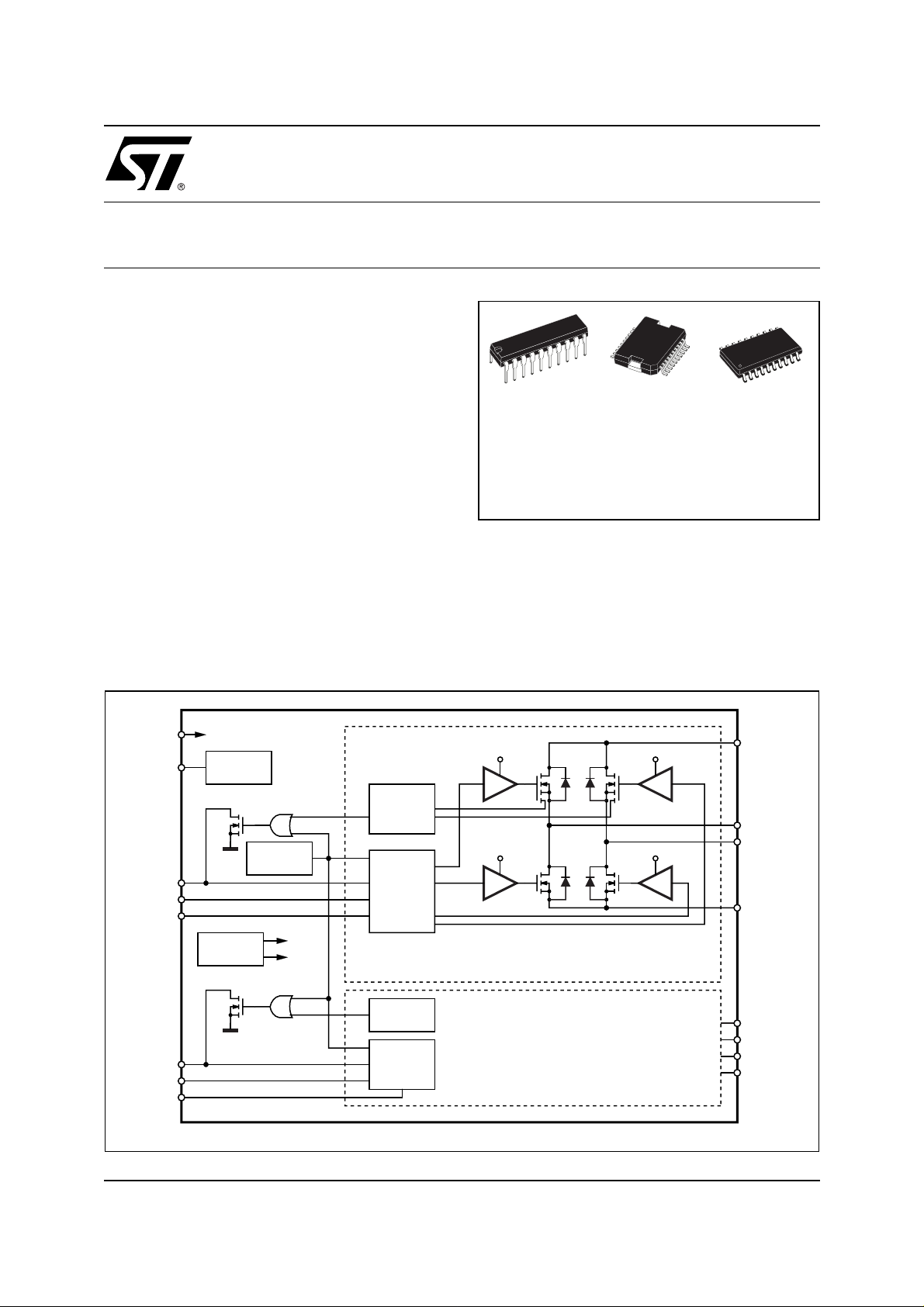
DESCRIPTION
The L6225 is a DMOS Dual Full Bridge designed for
motor control applications, realized in MultiPower-
0.73Ω TYP. VALUE @ Tj = 25 °C
DS(ON)
L6225
PowerDIP20
(16+2+2)
BCD technology, which combines isolated DMOS
Power Transistors with CMOS and bipolar c ir cuits on
the same chip. Available in PowerDIP20 (16+2+2),
PowerSO20 and SO20(16+2+2) packages, the
L6225 features a non-dissipative protection of the
high side PowerMOSFETs and thermal shutdown.
PowerSO20
ORDERING NUMBERS:
L6225N (PowerDIP 20)
L6225PD (PowerSO20)
L6225D (SO20)
SO20
(16+2+2)
BLOCK DIAGRAM
VBOOT
VCP
EN
IN1
IN2
EN
IN1
IN2
A
A
A
B
B
B
V
BOOT
CHARGE
PUMP
VOLTAGE
REGULA TOR
OCD
THERMAL
PROTECTION
10V
5V
OCD
VS
V
BOOT
OVER
A
B
CURRENT
DETECTION
GA TE
LOGIC
OVER
CURRENT
DETECTION
GA TE
LOGIC
10V 10V
V
BOOT
BRIDGE A
BRIDGE B
A
OUT1
OUT2
SENSE
V
S
B
OUT1
OUT2
SENSE
A
A
A
B
B
B
September 2003
D99IN1091A
1/20

L6225
ABSOLUTE MAXIMUM RATINGS
Symbol Parameter Test conditions Value Unit
V
S
V
OD
V
BOOT
V
IN,VEN
V
SENSEA,
V
SENSEB
I
S(peak)
Supply Voltage
Differential Voltage between
VSA, OUT1A, OUT2A, SENSEA and
VSB, OUT1B, OUT2B, SENSE
Bootstrap Peak Voltage
Input and Enable Voltage Range -0.3 to +7 V
Voltage Range at pins SENSEA
and SENSE
B
Pulsed Supply Current (for each
pin), internally limited by the
V
S
VSA =
VSB = V
VSA =
VSB = VS = 60V;
V
SENSEA
B
VSA =
VSB = V
= V
S
SENSEB
S
= GND
60 V
60 V
VS + 10 V
-1 to +4 V
VSA =
t
PULSE
VSB = VS;
< 1ms
3.55 A
overcurrent protection
I
S
, T
T
stg
RMS Supply Current (for each
pin)
V
S
Storage and Operating
OP
VSA =
VSB = V
S
1.4 A
-40 to 150 °C
Temperature Range
RECOMMENDED OPERATING CONDITIONS
Symbol Parameter Test Conditions MIN MAX Unit
V
V
OD
V
SENSEA,
V
SENSEB
I
OUT
T
f
sw
Supply Voltage
S
Differential Voltage Between
VSA, OUT1A, OUT2A, SENSEA and
VSB, OUT1B, OUT2B, SENSE
Voltage Range at pins SENSEA
and SENSE
B
VSA =
VSA =
V
SENSEA
B
(pulsed tW < trr)
(DC)
VSB = V
VSB = VS;
= V
SENSEB
S
852V
-6
-1
RMS Output Current 1.4 A
Operating Junction Temperature -25 +125 °C
j
Switching Frequency 100 KHz
52 V
6
1
V
V
2/20
L6225
THERMA L D ATA
Symbol Description PowerDIP20 SO20 PowerSO20 Unit
R
th-j-pins
R
th-j-case
R
th-j-amb1
R
th-j-amb1
R
th-j-amb1
R
th-j-amb2
(1) Mounted on a multi-layer FR4 PCB with a dissipati ng copper surface on the bottom side of 6cm2 (with a thickness of 35µm).
(2) Mounted on a multi-layer FR4 PCB with a dissipati ng copper surface on the top side of 6cm2 (with a thic kness of 35µm ).
(3) Mounted on a multi-layer FR4 PCB with a dissipating copper surface on the top side of 6cm2 (with a thickness of 35µm), 16 via holes
and a groun d l ayer.
(4) Mounted on a multi-layer FR4 PCB without any hea t s i nking surfac e on the board.
PIN CONNECTIONS (Top View)
MaximumThermal Resistance Junction-Pins 13 15 - °C/W
Maximum Thermal Resistance Junction-Case - - 2 °C/W
MaximumThermal Resistance Junction-Ambient
Maximum Thermal Resistance Junction-Ambient
MaximumThermal Resistance Junction-Ambient
Maximum Thermal Resistance Junction-Ambient
1
2
3
4
41 52 - °C/W
--36°C/W
--16°C/W
57 78 63 °C/W
IN1
IN2
SENSE
OUT1
GND GND
GND
OUT1
SENSE
IN1
IN2
1
A
2
A
3
A
4
A
5
6
7
B
8
B
9
B
10
B
D99IN1093A
20
19
18
17
16
14
13
12
11
EN
A
VCP
OUT2
VS
A
GND15
VS
B
OUT2
VBOOT
EN
B
GND GND
VS
A
OUT2
VCP
EN
IN1
IN2
B
SENSE
OUT1
GND
PowerDIP20/SO20
(5) The slug is internally connected to pins 1,10,11 and 20 (GND pins).
1
A
A
2
3
4
A
A
A
A
A
5
6
7
8
9
D99IN1092A
PowerSO20
(5)
20
19
18
17
16
15
14
13
12
11
VS
B
OUT2
VBOOT
EN
B
IN2
B
IN1
B
SENSE
OUT1
GND10
B
B
B
3/20

L6225
PIN DESCRIPTION
PACKA GE
SO20/
PowerDIP20
PowerSO20
Name Type Function
PIN # PIN #
1 6 IN1
2 7 IN2
3 8 SENSE
A
A
Logic Input Bridge A Logic Input 1.
Logic Input Bridge A Logic Input 2.
Power Supply Bridge A Source Pin. This pin must be connected to Power
A
Ground directly or through a sensing power resistor.
4 9 OUT1
5, 6, 15, 16 1, 10, 11,
20
GND GND Signal Ground terminals. In PowerDIP and SO packages,
Power Output Bridge A Output 1.
A
these pins are also used for heat dissipation toward the
PCB.
7 12 OUT1
8 13 SENSE
Power Output Bridge B Output 1.
B
Power Supply Bridge B Source Pin. This pin must be connected to Power
B
Ground directly or through a sensing power resistor.
9 14 IN1
10 15 IN2
11 16 EN
B
B
B
Logic Input Bridge B Logic Input 1.
Logic Input Bridge B Logic Input 2.
(6)
Logic Input
Bridge B Enable. LOW logic level switches OFF all Power
MOSFETs of Bridge B. This pin is also connected to the
collector of the Overcurrent and Thermal Protection
transistor to implement over current protection.
If not used, it has to be connected to +5V through a
resistor.
12 17 VBOOT Supply
Voltage
13 18 OUT2
14 19 VS
Power Output Bridge B Output 2.
B
Power Supply Bridge B Power Supply Voltage. It must be connected to
B
Bootstrap Voltage needed for driving the upper
PowerMOSFETs of both Bridge A and Bridge B.
the supply voltage together with pin VS
17 2 VS
Power Supply Bridge A Power Supply Voltage. It must be connected to
A
the supply voltage together with pin VS
18 3 OUT2
Power Output Bridge A Output 2.
A
19 4 VCP Output Charge Pump Oscillator Output.
20 5 EN
A
Logic Input
(6)
Bridge A Enable. LOW logic level switches OFF all Power
MOSFETs of Bridge A. This pin is also connected to the
collector of the Overcurrent and Thermal Protection
transistor to implement over current protection.
If not used, it has to be connected to +5V through a
resistor.
.
A
.
B
(6) Also connect ed at the output dra i n o f the Overcurren t and Thermal prot ection MOSF E T . Therefore, it has to be driven putting in series a
resistor with a value in the range of 2.2kΩ - 180K Ω , recommend e d 100kΩ
4/20
L6225
ELECTRICAL CHARACTERISTICS
(T
= 25 °C, Vs = 48V, unless otherwise specified)
amb
Symbol Parameter Test Conditions Min Typ Max Unit
V
Sth(ON)
V
Sth(OFF)
T
j(OFF)
Turn-on Threshold 5.8 6.3 6.8 V
Turn-off Threshold 5 5.5 6 V
I
Quiescent Supply Current All Bridges OFF;
S
Thermal Shutdown Temperature 165 °C
Output DMOS Transistors
R
DS(ON)
High-Side + Low-Side Switch ON
Resistance
I
DSS
Leakage Current EN = Low; OUT = V
Source Drain Diodes
V
Forward ON Voltage ISD = 1.4A, EN = LOW 1.15 1.3 V
SD
t
Reverse Recovery Time If = 1.4A 300 ns
rr
Forward Recovery Time 200 ns
t
fr
Logic Input
V
Low level logic input voltage -0.3 0.8 V
IL
= -25°C to 125°C
T
j
(7)
Tj = 25 °C 1.47 1.69 Ω
510mA
=125 °C
T
j
(7)
S
2.35 2.70 Ω
2mA
EN = Low; OUT = GND -0.3 mA
V
V
th(ON)
V
th(OFF)
V
th(HYS)
High level logic input voltage 2 7 V
IH
I
Low Level Logic Input Current GND Logic Input Voltage -10 µA
IL
I
High Level Logic Input Current 7V Logic Input Voltage 10 µA
IH
Turn-on Input Threshold 1.8 2.0 V
Turn-off Input Threshold 0.8 1.3 V
Input Threshold Hysteresis 0.25 0.5 V
Switching Characteristics
t
D(on)EN
t
D(on)IN
t
RISE
t
D(off)EN
t
D(off)IN
t
FALL
Enable to out turn ON delay time
Input to out turn ON delay time I
Output rise time
Enable to out turn OFF delay time
Input to out turn OFF delay time
Output Fall Time
(8)
(8)
(8)
I
=1.4A, Resistive Load 500 800 ns
LOAD
=1.4A, Resistive Load
LOAD
(dead time included)
I
=1.4A, Resistive Load 40 250 ns
LOAD
(8)
I
=1.4A, Resistive Load 500 800 1000 ns
LOAD
I
=1.4A, Resistive Load 500 800 1000 ns
LOAD
I
=1.4A, Resistive Load 40 250 ns
LOAD
1.9 µs
5/20
L6225
ELECTRICAL CHARACTERISTICS (continued)
(T
= 25 °C, Vs = 48V, unless otherwise specified)
amb
Symbol Parameter Test Conditions Min Typ Max Unit
t
Dead Time Protection 0.5 1 µs
dt
f
CP
Charge pump frequency
-25°C<Tj <125°C 0.6 1 MHz
Over Current Protection
I
SOVER
R
OPDR
t
OCD(ON)
t
OCD(OFF)
(7) Tested at 25°C in a restricted range and guaranteed by characterization.
(8) See Fig. 1.
(9) See Fig. 2.
Input Supply Overcurrent
Protection Threshold
= -25°C to 125°C
T
j
Open Drain ON Resistance I = 4mA 40 60 Ω
OCD Turn-on Delay Time (9) I = 4mA; CEN < 100pF 200 ns
OCD Turn-off Delay Time (9) I = 4mA; CEN < 100pF 100 ns
Figure 1. Switching Characteristic Definition
EN
V
th(ON)
V
th(OFF)
I
OUT
(7)
2 2.8 3.55 A
t
6/20
90%
10%
D01IN1316
t
D(OFF)EN
t
FALL
t
D(ON)EN
t
RISE
t
 Loading...