

DMOS DRIVER FOR BIPOLAR STEPPER MOTOR
■
OPERATING SUPPLY VOLTAGE FROM 8 TO 52V
■ 5.6A OUTPUT PEAK CURRENT (2.8A RMS)
■ R
■ OPERATING FREQUENCY UP TO 100KHz
■ NON DISSIPATIVE OVERCURRENT
PROTECTION
■ DUAL INDEPENDENT CONSTANT t
CURRENT CONTROLLERS
■ FAST/SLOW DECAY MODE SELECTION
■ FAST DECAY QUASI-SYNCHRONOUS
RECTIFICATION
■ DECODING LOGIC FOR STEPPER MOTOR
FULL AND HALF STEP DRIVE
■ CROSS CONDUCTION PROTECTION
■ THERMAL SHUTDOWN
■ UNDER VOLTAGE LOCKOUT
■
INTEGRATED FAST FREE WHEELING DIODES
TYPICAL APPLICATIONS
■ BIPOLAR STEPPER MOTOR
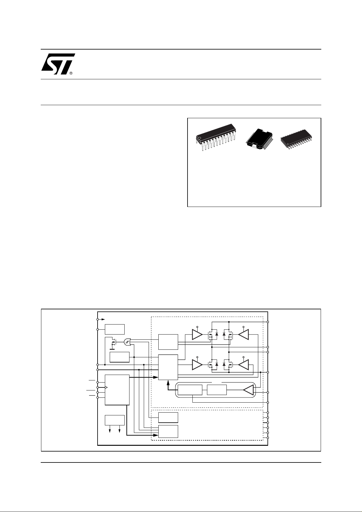
DESCRIPTION
The L6208 is a DMOS Fully Integrated Stepper Motor
Driver with non-dissipative Overcurrent Protection,
realized in MultiPower-BCD technology, which com-
BLOCK DIAGRAM
0.3Ω TYP. VA LUE @ Tj = 25°C
DS(ON)
OFF
PWM
L6208
PowerDIP24
PowerSO36
(20+2+2)
ORDERING NUMBERS:
L6208N (PowerDIP24)
L6208PD (PowerSO36)
L6208D (SO24)
bines isolated DMOS Power Transistors with CMOS
and bipolar circuits on the same chip. The device includes all the circuitry needed to drive a two-phase
bipolar stepper motor including: a dual DMOS Full
Bridge, the constan t off tim e PWM Current C ontroller
that performs the chopping regulation and the Phase
Sequence Generator, that generates the stepping
sequence. Available in PowerDIP24 (20+2+2),
PowerSO36 and SO24 (20+2+2) packages, the
L6208 features a non-dissipative overcurrent protection on the high side Power MOSFETs and thermal
shutdown.
SO24
(20+2+2)
September 2003
VBOOT
VCP
CONTROL
HALF/FULL
CLOCK
RESET
CW/CCW
V
BOOT
CHARGE
PUMP
THERMAL
EN
PROTECTION
STEPPING
SEQUENCE
GENERATION
VOLTAGE
REGULAT OR
5V10V
OCD
OCD
A
B
OVER
CURRENT
DETECTION
GATE
LOGIC
OVER
CURRENT
DETECTION
GATE
LOGIC
V
BOOT
10V 10V
ONE SHOT
MONOSTABLE
MASKING
PWM
TIME
V
BOOT
SENSE
COMPARATOR
BRIDGE A
BRIDGE B
+
-
D01IN1225
VS
A
OUT1
OUT2
SENSE
VREF
RC
A
VS
B
OUT1
OUT2
SENSE
VREF
RC
B
A
A
A
A
B
B
B
B
1/27

L6208
ABSOLUTE MAXIMUM RATINGS
Symbol Parameter Test conditions Value Unit
V
S
V
OD
V
BOOT
V
IN,VEN
V
REFA
V
REFB
V
RCA, VRCB
V
SENSEA,
V
SENSEB
I
S(peak)
I
S
, T
T
stg
Supply Voltage
Differential Voltage between
VSA, OUT1A, OUT2A, SENSEA and
VSB, OUT1B, OUT2B, SENSE
Bootstrap Peak Voltage
VSA =
VSB = V
VSA =
VSB = VS = 60V;
V
SENSEA
B
VSA =
VSB = V
= V
S
SENSEB
S
= GND
60 V
60 V
VS + 10 V
Input and Enable Voltage Range -0.3 to +7 V
,
Voltage Range at pins V
and V
REFB
REFA
Voltage Range at pins RCA and
RC
B
Voltage Range at pins SENSEA
and SENSE
B
Pulsed Supply Current (for each
pin), internally limited by the
V
S
VSA =
t
PULSE
VSB = VS;
< 1ms
-0.3 to +7 V
-0.3 to +7 V
-1 to +4 V
7.1 A
overcurrent protection
RMS Supply Current (for each
pin)
V
S
Storage and Operating
OP
VSA =
VSB = V
S
2.8 A
-40 to 150 °C
Temperature Range
RECOMMENDED OPERATING CONDITIONS
Symbol Parameter Test Conditions MIN MAX Unit
V
V
OD
V
REFA
V
REFB
V
SENSEA,
V
SENSEB
I
OUT
T
f
sw
Supply Voltage
S
Differential Voltage Between
VSA, OUT1A, OUT2A, SENSEA and
VSB, OUT1B, OUT2B, SENSE
,
Voltage Range at pins V
and V
REFB
Voltage Range at pins SENSEA
and SENSE
B
REFA
VSA =
VSA =
V
SENSEA
B
(pulsed tW < trr)
(DC)
VSB = V
VSB = VS;
= V
SENSEB
S
852V
-0.1 5 V
-6
-1
RMS Output Current 2.8 A
Operating Junction Temperature -25 +125 °C
j
Switching Frequency 100 KHz
52 V
6
1
V
V
2/27
L6208
THERMA L D ATA
Symbol Description PowerDIP24 SO24 PowerSO36 Unit
R
th-j-pins
R
th-j-case
R
th-j-amb1
R
th-j-amb1
R
th-j-amb1
R
th-j-amb2
(1) Mounted on a multi-layer FR4 PCB with a dissipati ng copper surface on the bottom side of 6cm2 (with a thickness of 35µm).
(2) Mounted on a multi-layer FR4 PCB with a dissipati ng copper surface on the top side of 6cm2 (with a thic kness of 35µm ).
(3) Mounted on a multi-layer FR4 PCB with a dissipating copper surface on the top side of 6cm2 (with a thickness of 35µm), 16 via holes
and a groun d l ayer.
(4) Mounted on a multi-layer FR4 PCB without any hea t s i nking surfac e on the board.
Maximum Thermal Resistance Junction-Pins 18 14 - °C/W
Maximum Thermal Resistance Junction-Case - - 1 °C/W
Maximum Thermal Resistance Junction-Ambient
Maximum Thermal Resistance Junction-Ambient
Maximum Thermal Resistance Junction-Ambient
Maximum Thermal Resistance Junction-Ambient
(1)
(2)
(3)
(4)
43 51 - °C/W
--35°C/W
--15°C/W
58 77 62 °C/W
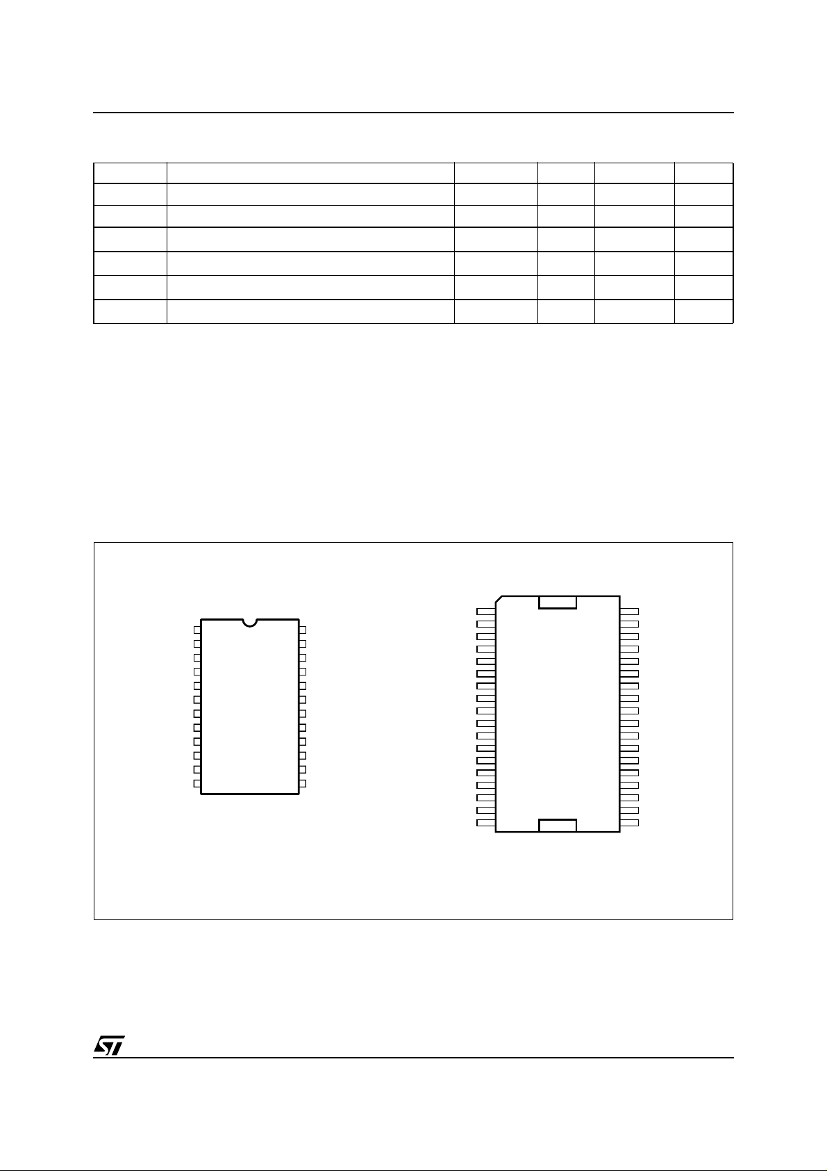
PIN CONNECTIONS (Top View)
RC
GND
GND
RC
1
2
3
A
4
A
5
A
6
7
8
B
9
B
10
B
11
B
12
D99IN1083
CLOCK
CW/CCW
SENSE
OUT1
OUT1
SENSE
VREF
HALF/FULL
PowerDIP24/SO24
(5) The slug is internally connected to pins 1,18,19 and 36 (GND pins).
VREF
24
23
22
21
20
18
17
16
15
14
13
A
RESET
VCP
OUT2
A
VS
A
GND19
GND
VS
B
OUT2
B
VBOOT
EN
CONTROL
GND
N.C.
N.C.
VS
OUT2
N.C. N.C.
VCP
RESET
VREF
CLOCK
CW/CCW
SENSE
RC
N.C.
OUT1
N.C.
N.C. N.C.
GND GND
1
2
3
4
A
5
A
6
7
8
9
A
10 27
11
12
A
13 24
A
14
15
A
16
17
18
D99IN1084
PowerSO36
36
35
34
33
32
31
30
29
28
26
25
23
22
21
20
19
(5)
GND
N.C.
N.C.
VS
B
OUT2
B
VBOOT
EN
CONTROL
HALF/FULL
VREF
B
SENSE
B
RC
B
N.C.
OUT1
B
N.C.
3/27

L6208
PIN DESCRIPTION
PACKAGE
SO24/
PowerDIP24
PowerSO36
Name Type Function
PIN # PIN #
1 10 CLOCK Logic Input Step Clock input. The state machine makes one step on
each rising edge.
2 11 CW/CCW Logic Input Selects the direction of the rotation. HIGH logic level sets
clockwise direction, whereas LOW logic level sets
counterclockwise direction.
If not used, it has to be connected to GND or +5V.
3 12 SENSE
Power Supply Bridge A Source Pin. This pin must be connected to Power
A
Ground through a sensing power resistor.
413RC
A
RC Pin RC Network Pin. A parallel RC network connected
between this pin and ground sets the Current Controller
OFF-Time of the Bridge A.
5 15 OUT1
6, 7,
18, 19
1, 18,
19, 36
GND GND Ground terminals. In PowerDIP24 and SO24 packages,
Power Output Bridge A Output 1.
A
these pins are also used for heat dissipation toward the
PCB. On PowerSO36 package the slug is connected to
these pins.
8 22 OUT1
924RC
Power Output Bridge B Output 1.
B
B
RC Pin RC Network Pin. A parallel RC network connected
between this pin and ground sets the Current Controller
OFF-Time of the Bridge B.
10 25 SENSE
Power Supply Bridge B Source Pin. This pin must be connected to Power
B
Ground through a sensing power resistor.
11 26 VREF
Analog Input Bridge B Current Controller Reference Voltage.
B
Do not leave this pin open or connected to GND.
12 27 HALF/FULL Logic Input Step Mode Selector. HIGH logic level sets HALF STEP
Mode, LOW logic level sets FULL STEP Mode.
If not used, it has to be connected to GND or +5V.
13 28 CONTROL Logic Input Decay Mode Selector. HIGH logic level sets SLOW DECAY
Mode. LOW logic level sets FAST DECAY Mode.
If not used, it has to be connected to GND or +5V.
(6)
14 29 EN
Logic Input
Chip Enable. LOW logic level switches OFF all Power
MOSFETs of both Bridge A and Bridge B. This pin is also
connected to the collector of the Overcurrent and Thermal
Protection to implement over current protection.
If not used, it has to be connected to +5V through a
resistor.
15 30 VBOOT Supply
Voltage
16 32 OUT2
17 33 VS
20 4 VS
Power Output Bridge B Output 2.
B
Power Supply Bridge B Power Supply Voltage. It must be connected to
B
Power Supply Bridge A Power Supply Voltage. It must be connected to
A
Bootstrap Voltage needed for driving the upper Power
MOSFETs of both Bridge A and Bridge B.
the Supply Voltage together with pin VS
the Supply Voltage together with pin VS
A
B
4/27

L6208
PIN DESCRIPTION
(continued)
PACKAGE
SO24/
PowerDIP24
PowerSO36
Name Type Function
PIN # PIN #
21 5 OUT2
Power Output Bridge A Output 2.
A
22 7 VCP Output Charge Pump Oscillator Output.
23 8 RESET Logic Input Reset Pin. LOW logic level restores the
Home
State
(State 1) on the Phase Sequence Generator State
Machine.
If not used, it has to be connected to +5V.
24 9 VREF
Analog Input Bridge A Current Controller Reference Voltage.
A
Do not leave this pin open or connected to GND.
(6) Also connected at the output drain of the Over current and Thermal protection MOSFET. Therefore, it has to be driven putting in series
a resistor with a value in the range of 2.2KΩ - 180KΩ, recommended 100KΩ.
ELECTRICAL CHARACTERISTICS
(T
= 25°C, Vs = 48V, unless otherwise specified)
amb
Symbol Parameter Test Conditions Min Typ Max Unit
V
Sth(ON)
V
Sth(OFF)
Turn-on Threshold 6.6 7 7.4 V
Turn-off Threshold 5.6 6 6.4 V
I
Quiescent Supply Current All Bridges OFF;
S
T
j(OFF)
= -25°C to 125°C
T
j
Thermal Shutdown Temperature 165 °C
(7)
Output DMOS Transistors
R
DS(ON)
I
High-Side Switch ON Resistance Tj = 25 °C 0.34 0.4 Ω
T
=125 °C
j
Low-Side Switch ON Resistance T
Leakage Current EN = Low; OUT = V
DSS
= 25 °C 0.28 0.34 Ω
j
T
=125 °C
j
(7)
(7)
S
EN = Low; OUT = GND -0.15 mA
Source Drain Diodes
V
Forward ON Voltage ISD = 2.8A, EN = LOW 1.15 1.3 V
SD
t
Reverse Recovery Time If = 2.8A 300 ns
rr
Forward Recovery Time 200 ns
t
fr
Logic Inputs (EN, CONTROL, HALF/FULL, CLOCK, RESET, CW/CCW)
V
Low level logic input voltage -0.3 0.8 V
IL
510mA
0.53 0.59 Ω
0.47 0.53 Ω
2mA
V
High level logic input voltage 2 7 V
IH
5/27

L6208
ELECTRICAL CHARACTERISTICS (continued)
(T
= 25°C, Vs = 48V, unless otherwise specified)
amb
Symbol Parameter Test Conditions Min Typ Max Unit
I
Low Level Logic Input Current GND Logic Input Voltage -10 µA
IL
I
High Level Logic Input Current 7V Logic Input Voltage 10 µA
IH
V
th(ON)
V
th(OFF)
V
th(HYS)
Turn-on Input Threshold 1.8 2.0 V
Turn-off Input Threshold 0.8 1.3 V
Input Threshold Hysteresis 0.25 0.5 V
Switching Characteristics
t
D(ON)EN
t
D(OFF)EN
t
RISE
t
FALL
t
DCLK
t
CLK(min)L
t
CLK(min)
f
t
S(MIN)
t
H(MIN)
t
R(MIN)
Enable to Output Turn-on Delay
(8)
Time
Enable to Output Turn-off Delay
(8)
Time
Output Rise Time
Output Fall Time
Clock to Output Delay Time
Minimum Clock Time
Minimum Clock Time
H
Clock Frequency 100 KHz
CLK
Minimum Set-up Time
Minimum Hold Time
Minimum Reset Time
(8)
(8)
(10)
(10)
(11)
(11)
(11)
(9)
I
=2.8A, Resistive Load 100 250 400 ns
LOAD
I
=2.8A, Resistive Load 300 550 800 ns
LOAD
I
=2.8A, Resistive Load 40 250 ns
LOAD
I
=2.8A, Resistive Load 40 250 ns
LOAD
I
=2.8A, Resistive Load 2 µs
LOAD
1µs
1µs
1µs
1µs
1µs
t
RCLK(MIN
Minimum Reset to Clock Delay
)
t
DT
f
CP
(11)
Time
Dead Time Protection 0.5 1 µs
Charge Pump Frequency
PWM Comparator and Monostable
I
RCA, IRCB
V
Source Current at pins RCA and
RC
B
Offset Voltage on Sense
offset
Comparator
t
PROP
t
BLANK
Turn OFF Propagation Delay
Internal Blanking Time on
SENSE pins
t
ON(MIN)
Minimum On Time 1.5 2 µs
6/27
1µs
Tj = -25°C to 125°C
V
= V
RCA
V
REFA, VREFB
(12)
RCB
(7)
0.6 1 MHz
= 2.5V 3.5 5.5 mA
= 0.5V ±5 mV
500 ns
1µs
L6208
ELECTRICAL CHARACTERISTICS (continued)
(T
= 25°C, Vs = 48V, unless otherwise specified)
amb
Symbol Parameter Test Conditions Min Typ Max Unit
t
I
BIAS
PWM Recirculation Time R
OFF
Input Bias Current at pins VREFA
OFF
R
OFF
= 20KΩ; C
= 100KΩ; C
OFF
OFF
= 1nF
= 1nF
and VREFB
Over Current Protection
I
SOVER
R
OPDR
t
OCD(ON)
t
OCD(OFF)
(7) Tested at 25°C in a restricted range and guaranteed by characterization.
(8) See Fig. 1.
(9) See Fig. 2.
(10) See Fig. 3.
(11) See Fig. 4.
(12) Measured applyin g a voltage of 1V to pi n SENSE and a voltage drop fr om 2V to 0V to pin VR EF.
(13) See Fig. 5.
Input Supply Overcurrent
Protection Threshold
= -25°C to 125°C
T
j
Open Drain ON Resistance I = 4mA 40 60 Ω
OCD Turn-on Delay Time (13) I = 4mA; CEN < 100pF 200 ns
OCD Turn-off Delay Time (13) I = 4mA; CEN < 100pF 100 ns
(7)
4 5.6 7.1 A
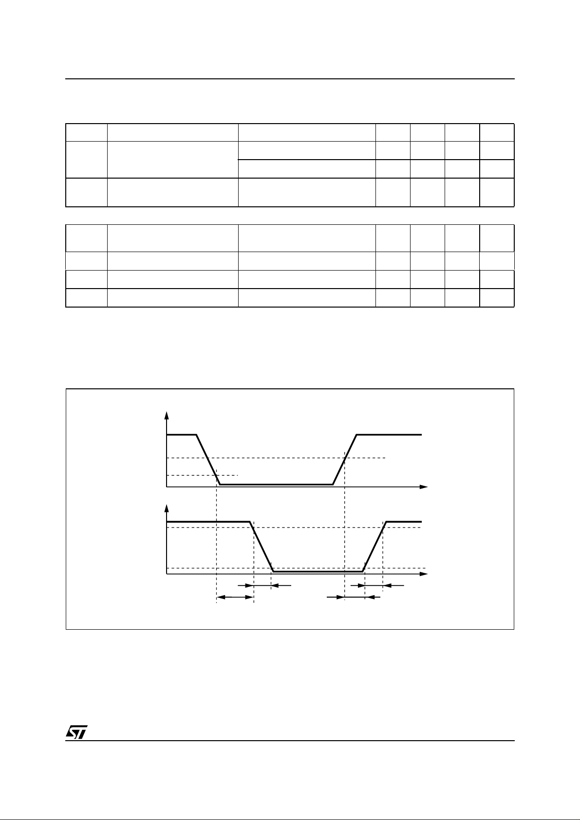
Figure 1. Switching Characteristic Definition
EN
13
61
µs
µs
10 µA
V
th(ON)
V
th(OFF)
I
OUT
90%
10%
D01IN1316
t
D(OFF)EN
t
FALL
t
D(ON)EN
t
RISE
t
t
7/27
L6208
Figure 2. Clock to Output Delay Time
CLOCK
I
OUT
V
th(ON)
t
D01IN1317
Figure 3. Minimum Timing Definition; Clock Input
CLOCK
V
V
th(OFF)
th(ON)
t
CLK(MIN)L
Figure 4. Minimum Timing Definition; Logic Inputs
CLOCK
LOGIC INPUTS
V
th(ON)
t
V
th(OFF)
t
CLK(MIN)H
t
DCLK
D01IN1318
8/27
RESET
V
th(OFF)
V
th(ON)
t
R(MIN)
t
S(MIN)
t
RCLK(MIN)
t
H(MIN)
D01IN1319
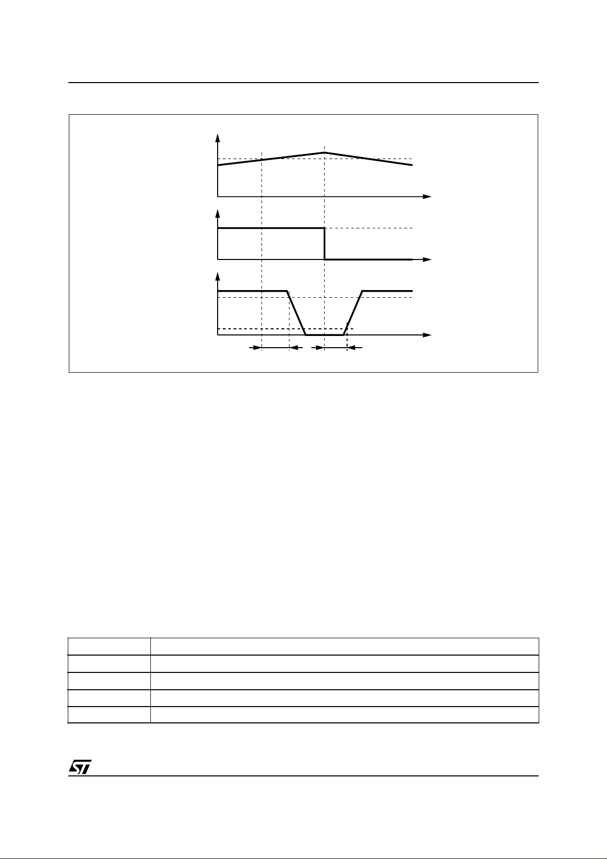
Figure 5. Ove rcurrent Detect i on Timi ng Definition
I
OUT
I
SOVER
ON
BRIDGE
OFF
V
EN
90%
10%
L6208
t
OCD(ON)
t
OCD(OFF)
D02IN1399
CIRCUIT DESCRIPTION
POWER STAGES and CHARGE PUMP
The L6208 integrates two independent Power MOS Full Bridges. Each Power MOS has an R
DS(ON)
= 0.3Ω (typical value @ 25°C), with i ntrinsic fast freew heeling diode. Switchi ng patterns are generated by the PWM Current
Controller and the Phase Sequence Generator (see below). Cross conduction protection is achieved using a
dead time (t
= 1µs typical value) between the sw itch off and s witch on of tw o Power MOSFETSs in one leg of
DT
a bridge.
Pins VS
voltage in the range from 8V to 52V. It has to be noticed that the R
and VSB MUST be connected together to the supply voltage VS. The device operates with a supply
A
increases of some percents when the
DS(ON)
supply voltage is in the range from 8V to 12V (see Fig. 34 and 35).
Using N-Channel Power MOS for the upper transistors in the bridge requires a gate drive voltage above the
power supply vol tage. The bootstrapped supply voltage V
is obtained through an internal Oscillator and few
BOOT
external components to realize a charge pump circuit as shown in Figure 6. The oscillator output (VCP) is a
square wave at 600KHz (typic al) with 10V amplitud e. Recommended va lues/part number s for the c harge pump
circuit are shown in Table 1.
Table 1. Charge Pump External Components Values
C
BOOT
C
P
R
P
D1 1N4148
D2 1N4148
220nF
10nF
100Ω
9/27

L6208
0
Figure 6. Char ge Pump Circu it
V
S
D1
D2
R
P
C
P
VCP VBOOT VS
LOGIC INPUTS
Pins CONTROL, HALF/FULL, CLOCK, RESET and CW/CCW are TTL/CMOS and uC compatible logic inputs.
The internal structure is shown in Fig. 7. Typical value for turn-on and turn-off thresholds are respectively
V
th(ON)
= 1.8V and V
th(OFF)
= 1.3V.
Pin EN (Enable) has identical input structure with the exception that the drain of the Overcurrent and thermal
protection MOSFET i s also c onnected to this pin. Due to this connectio n some car e needs to be taken in driv ing
this pin. The EN input may be driven in one of two configurations as shown in Fig. 8 or 9. If driven by an open
drain (collector) structure, a pull-up resistor R
driver is a standard Push-Pull structure the resistor R
9. The resistor R
C
are respectively 100KΩ and 5.6nF. More information on selecting the values is found in the Overcurrent
EN
should be chosen in the range from 2.2KΩ to 180KΩ. Recommended values for REN and
EN
Protection section.
C
BOOT
B
D01IN1328
VS
A
and a capacitor CEN are connected as shown in Fig. 8. If the
EN
and the capacitor CEN are connected as shown in Fig.
EN
Figure 7. Logi c Inp ut s I nte rn a l St ructure
Figure 8. EN Pi n Open Collector D ri vin g
5V
OPEN
COLLECTOR
OUTPUT
Figure 9. EN Pin Pu s h-P ull Driving
R
PUSH-PULL
OUTPUT
EN
ESD
PROTECTION
R
EN
EN
C
EN
PROTECTION
EN
C
EN
PROTECTION
5V
D01IN1329
5V
ESD
D01IN133
5V
ESD
D01IN1331
10/27

L6208
PWM CURRENT CONTROL
The L6208 includes a constant off time PWM current controller for each of the two bridges. The current control
circuit senses the bridge current by sensing the voltage drop across an external sense resistor connected between the source of the two lower power MOS transistors and ground, as shown in Figure 10. As the current in
the motor builds up the voltage across the sense resistor increases proportionally. When the voltage drop
across the sense resistor becomes greater than the voltage at the reference input (VREF
comparator triggers the monostable switching the bridge off. The power MOS remain off for the time set by the
monostable and the motor current recirculates as defined by the selected decay mode, described in the next
section. When the monostable times out the bridge w ill again turn on. S ince the inter nal dead time, us ed to prevent cross c onduction in the bridge, delays the turn on of the power MOS, the effecti ve off time is the s um of the
monostable time plus the dead time.
Figure 10. PWM Current Controller Simplified Schematic
(or B)
VS
A
TO GATE LOGIC
BLANKING TIME
MONOST ABLE
1µs
FROM THE
LOW-SIDE
GATE DRIVERS
or VREFB) the sense
A
5mA
MONOSTABLE
S
(0) (1)
5V
RC
C
OFF
R
Q
R
-
+
2.5V
A(or B)
OFF
SET
BLANKER
SENSE
COMPARATOR
COMPARATOR
OUTPUT
DRIVERS
+
DEAD TIME
+
-
VREF
2H 1H
2L 1L
A(or B)
R
DRIVERS
DEAD TIME
SENSE
+
SENSE
A(or B)
OUT2
OUT1
I
OUT
A(or B)
A(or B)
D01IN1332
2 PHASE
STEPPER MOTOR
Figure 11 shows the typical operating waveforms of the output current, the voltage drop across the sensing resistor, the RC pin vol tage and the status of the bridge. More d etails regarding the S ynchronous Rectificati on and
the output stage configuration are included in the next section.
Immediately after the Power MOS turns on, a high peak current flows through the sensing resistor due to the
reverse recovery of the freewheeling diodes. The L6208 provides a 1
µ
s Blanking Time t
that inhibits the
BLANK
comparator output so that this current spike cannot prematurely re-trigger the monostable.
11/27

L6208
Figure 11. Output Current Regulation Waveforms
I
OUT
V
REF
R
SENSE
V
SENSE
V
REF
0
V
RC
5V
2.5V
ON
SYNCHRONOUS OR QUASI
SYNCHRONOUS RECTIFICATION
OFF
D01IN1334
t
OFF
1µs t
BLANK
t
ON
t
1µs t
Slow Decay Slow Decay
Fast Decay
t
RCRISE
t
RCFALL
1µs t
DT
BC
DDA
Fast Decay
t
RCRISE
t
RCFALL
1µs t
BC
OFF
BLANK
DT
Figure 12 shows the magnitude of the Off Time t
calculated from the equations:
t
RCFALL
t
OFF
where R
20K
0.47nF ≤ C
t
DT
= 0.6 · R
= t
RCFALL
and C
OFF
Ω ≤
R
OFF
OFF
OFF
= 1µs (typical value)
· C
OFF
+ tDT = 0.6 · R
OFF
· C
OFF
+ t
OFF
are the external component values and tDT is the internally generated Dead Time with:
≤ 100K
Ω
≤ 100nF
Therefore:
t
OFF(MIN)
t
OFF(MAX)
These values allow a sufficient range of t
The capacitor value chosen for C
Rise Ti me t
= 6.6µs
= 6ms
to implement the drive circuit for most motors.
OFF
also affects the Rise Time t
will only be an issue if the capacitor is not completely charged before the next time the
RCRISE
OFF
monostable is triggered. Therefore, the on time t
be bigger than t
can not be smaller than the minimum on time t
12/27
for allowing a good current regulation by the PWM stage. Furthermore, the on time t
RCRISE
ON(MIN)
versu s C
OFF
DT
, which depends by motors and supply parameters, has to
ON
OFF
RCRISE
and R
values. It can be approximately
OFF
of the voltage at the pin RCOFF. The
.
ON

L6208
>1.5µs (typ. value)=
t
ONtON MIN()
t
ONtRCRISEtDT
t
RCRISE
= 600 · C
Figure 13 shows the lower limit for the on time tON for having a good PWM current regulation capacity. It has to
be said that t
than t
RCRISE
So, small C
is always bigger than t
ON
- tDT. In this last case the device continues to work but the off time t
value gives more flexibility for the applications (allows smaller on time and, therefore, higher
OFF
switching frequency), but, the smaller is the value for C
performance.
–>
OFF
ON(MIN)
because the device imposes this condition, but it can be smaller
is not more constant.
OFF
, the more influential will be the noises on the circuit
OFF
Figure 12. t
versus C
OFF
and R
OFF
4
1.10
3
1.10
100
toff [µs]
10
1
0.1 1 10 100
OFF
= 100kΩ
R
off
= 47kΩ
R
off
= 20kΩ
R
off
Coff [nF]
Figure 13. Area where tON can vary maintaining the PWM regulation.
100
10
ton(min) [µs]
1.5µs (typ. value)
1
0.1 1 10 100
Coff [nF]
13/27
L6208
DECAY MODES
The CONTROL input is used to select the behavior of the bridge during the off time. When the CONTROL pin
is low, the Fast Decay mode is selected and both transistors in the bridge are switched off during the off time.
When the CONTROL pin is high, th e S low De cay mode i s s elected and onl y th e low s ide trans istor of the bridge
is switched off during the off time.
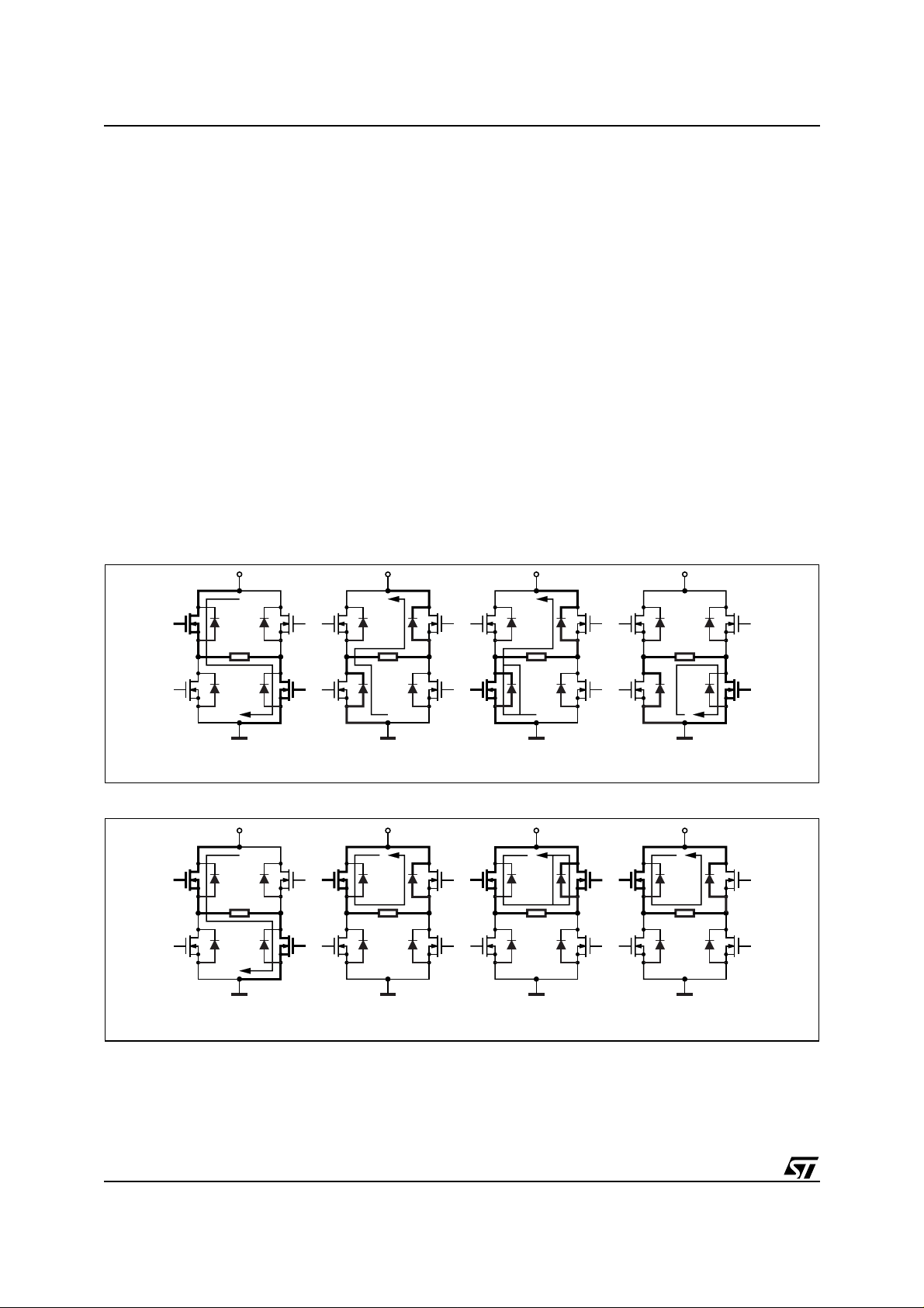
Figure 14 shows the operation of the bridge in the Fast Decay mode. At the start of the off time, both of the
power MOS are switched off and the current recirculates through the two opposite free wheeling diodes. The
current decays with a high di/dt since the voltage across the coil is essentially the power supply voltage. After
the dead time, the lower power MOS in parallel with the conducting diode is turned on in synchronous rectification mode. In applications where the motor current is low it is possible that the current can decay completely to
zero during the off time. At this point if both of the power MOS were operating in the synchronous rectification
mode it would then be possible for the current to build in the opposite direction. To prevent this only the lower
power MOS is operated in synchronous rectification mode. This operation is called Quasi-Synchronous Rectification Mode. When the monostable times out, the power MOS are turned on again after some delay set by the
dead time to prevent cross conduction.
Figure 15 shows the operation of the bridge i n the Slow Decay mode. At the start of the off ti me, the lower power
MOS is switched off and the current recirculates around the upper half of the bridge. Since the voltage across
the coil is low, the current decays slowly. After the dead time the upper power MOS is operated in the synchronous rectification mode. When the monostable times out, the lower power MOS is turned on again after some
delay set by the dead time to prevent cross conduction.
Figure 14. Fast Decay Mode Output Stage Configurations
A) ON TIME B) 1µs DEAD TIME C) QUASI-SYNCHRONOUS
D01IN1335
RECTIFICATION
D) 1µs SLOW DECAY
Figure 15. Slow Decay Mode Output Stage Configurations
A) ON TIME B) 1µs DEAD TIME C) SYNCHRONOUS
D01IN1336
RECTIFICATION
D) 1µs DEAD TIME
STEPPING SEQUENCE GENERATION
The phase sequence generator is a state machine that provides the phase and enable inputs for the two bri dges
to drive a stepper motor in e ither full step or half step. Two full step m odes ar e possibl e, the Nor mal Drive Mode
where both phases are energized each st ep and the Wave Drive Mode where only one phase is energized at a
14/27

L6208
time. The drive mode is selected by the HALF/FULL input and the current state of the sequence generator as
described below. A rising edge of the C LOCK input advances th e state machi ne to the next state. The dir ec tion
of rotation is set by the CW/CCW input. The RESET input resets the state machine to state.
HALF STEP MODE
A HIGH logic level on the HALF/FULL input selects Half Step Mode. Figure 16 shows the motor current waveforms and the state diagram for the Phase Sequencer Generator. At Start-Up or after a RESET the Phase Sequencer is at state 1. After each clock pulse the state changes follow ing the sequence 1,2,3,4,5,6,7,8,… if CW/
CCW is high (Clockwise movement) or 1,8,7,6,5,4,3,2,… if CW/CCW is low (Counterclockwise movement).
NORMAL DRIVE MODE (Full-step two-phase-on)
A LOW level on the HALF/FULL input selects the Full Step mode. When the low level is applied when the state
machine is at an ODD numbered state the Normal Drive Mode is selected. Figure Fig. 17 shows the motor current waveform state diagram for the state machine of the Phase Sequencer Generator. The Normal Drive Mode
can easily be selected by holding the HALF/FULL input low and applying a RESET. AT start -up or after a RESET the State Machine is in state1. While the HALF/FULL input is kept low, state changes following the sequence 1,3,5,7,… if CW/CCW is high (Clockwise movement) or 1,7,5,3,… if CW/CCW is low (Counterclockwise
movement).
WAVE DRIVE MODE (Full-step one-phase-on)
A LOW level on the pin HALF/FULL input selects the Full Step mode. When the low level is applied when the
state machine is at a n EVEN numbered s tate the W ave Driv e Mode is selected. Figure 18 shows the motor cur rent waveform and the state diagram for the state machine of the Phase Sequence Generator. To enter the
Wave Drive Mode the state machine must be in an EVEN numbered state. The most direct method to select the
Wave Drive Mode is to first apply a RESET, then while keeping the HALF/FULL input high apply one pulse to
the clock input then take the HALF/FULL input low. This sequence first forces the state machine to sate 1. The
clock pulse, with the HALF/FULL input high advances the state machine from state 1 to either state 2 or 8 depending on the CW/CCW input. Starting from this point, after each clock pulse (rising edge) will advance the
state machine following the s equence 2,4,6,8, … if CW/CCW is high (Clock wise movement) o r 8 ,6,4,2,… if CW/
CCW is low (Counterclockwise movement).
Figure 16. Half Step Mode
324 5
1 8 7
Start Up or Reset
Figure 17. Normal Drive Mode
35
2
17
Start Up or Reset
4
8
6
6
D01IN1320
D01IN1322
I
OUTA
I
OUTB
CLOCK
I
OUTA
I
OUTB
CLOCK
2345678
1
1
3571357
15/27

L6208
Figure 18. Wave Drive Mode
I
OUTA
4
35
I
D01IN1321
OUTB
CLOCK
4682468
2
2
17
Start Up or Reset
6
8
NON-DISSIPATIVE OVERCURRENT PROTECTION
The L6208 integrates an Overcurrent Detection Circuit (OCD). This circuit provides protection against a short
circuit to ground or between two phases of the bridge. With this inter nal over c urrent detection, the external current sense resistor normally used and its associated power dissipation are eliminated. Figure 19 shows a simplified schematic of the overcurrent detection circuit.
To implement the over current detection, a sensing element that deli ver s a small but precise fraction of the output current is implemented with each high side power MOS. Since this current is a small fraction of the output
current there is very little additional power dissipation. This current is compared with an internal reference current I
. When the output c urrent reaches the detec tion thresh old ( typi cally 5.6A ) the OCD com parator signal s
REF
a fault condition. When a fault condition is detected, the EN pin is pulled below the turn off threshold (1.3V typical) by an internal open drain MO S with a pull dow n capa bility of 4mA. B y using an exter nal R-C on the E N pin,
the off time before recovering normal operation can be easily programmed by means of the accurate thresholds
of the logic inputs.
Figure 19. Overcurrent Protection Simplified Schematic
POWER SENSE
1 cell
POWER DMOS
n cells
OVER TEMPERATURE
µC or LOGIC
V
DD
R
.EN
EN
C
.
EN
TO GATE
R
DS(ON)
40Ω TYP.
LOGIC
OCD
COMPARATOR
INTERNAL
OPEN-DRAIN
OCD
COMPARATOR
OUT1
A
I
I
/ n
1A
(I1A+I2A) / n
I
REF
FROM THE
BRIDGE B
VS
A
1A I2A
+
OUT2
A
POWER DMOS
I
/ n
2A
HIGH SIDE DMOSs OF
THE BRIDGE A
POWER SENSE
n cells
1 cell
16/27
D01IN1337

L6208
Figure 20 shows the Overcurrent Detection operation. The Disable Time t
DISABLE
before recovering normal operation can be easily programmed by means of the accurate thresholds of the logic inputs. It is affected whether by
C
and REN values and its magnitude is reported in Figure 21. The Delay Time t
EN
bridge when an overcurrent has been detected depends only by C
C
is also used for providing immunity to pin EN against fast transient noises. Therefore the value of C
EN
value. Its magnitude is reported in Figure 22.
EN
before turning off the
DELAY
EN
should be chosen as big as possi ble acc or ding to the maximum tolerable D elay Time and th e REN value should
be chosen according to the desired Disable Time.
The resistor R
should be chosen in the range from 2.2KΩ to 180KΩ. Recommended values for REN and C
EN
EN
are respectively 100KΩ and 5.6nF that allow obtaining 200µs Disable Time.
Figure 20. Overcurrent Protection Wavefo rms
I
OUT
I
SOVER
V
EN
V
DD
V
th(ON)
V
th(OFF)
ON
OCD
OFF
ON
BRIDGE
OFF
t
OCD(ON)
t
DELAY
t
EN(FALL)
t
D(OFF)EN
t
OCD(OFF)
V
EN(LOW)
t
DISABLE
t
EN(RISE)
t
D(ON)EN
D02IN1400
17/27
L6208
Figure 21. t
Figure 22. t
DISABLE
versus C
DELAY
versus CEN and R
3
3
1.10
1.10
100
100
[µs]
[µs]
DISABLE
DISABLE
t
t
10
10
1
1
110100
110100
EN (VDD
= 5V).
EN (VDD
= 5V).
REN= 220 k
REN= 220 k
Ω
Ω
CEN[n F]
CEN[nF]
REN= 100 k
REN= 100 k
Ω
Ω
R
R
R
R
R
R
EN
EN
EN
EN
EN
EN
= 47 k
= 47 k
= 33 k
= 33 k
= 10 k
= 10 k
Ω
Ω
Ω
Ω
Ω
Ω
10
s]
µ
1
tdelay [
0.1
1 10 100
Cen [nF]
THERMAL PROTECTION
In addition to the Ovecurrent Protection, the L6208 integrates a Thermal Protection for preventing the device
destruction in case of junction over temperature. It works sensing the die temperature by means of a sensible
element integrated in the die. The device switch-off when the junction temperature reaches 165°C (typ. value)
with 15°C hysteresis (typ. value).
18/27

L6208
APPLICATION INFORMATION
A typical Bipolar Stepper Motor Driver application using L6208 is shown in Fig. 23. Typical component values
for the application are shown in Table 2. A high quality ceramic capacitor in the range of 100 to 200 nF should
be placed between the power pins (VS
filtering on the power supply and reduce high frequency transients generated by the switching. The capacitor
connected from the EN input to ground sets the shut dow n time when an over current is detected ( see Overcur rent Protection). The two current sensing inputs (SENSE
resistors with a trace length as short as possible in the layout. The sense resistors should be non-inductive resistors to minimize the di/dt transients acro ss the resistor. To increase noise immunity, unused logic pins (except
EN) are best connected to 5V (High Logic Level) or GND (Low Logic Level) (see pin description). It is recommended to keep Power Ground and Signal Ground separated on PCB.
Table 2. Component Values for Typical Application
C
1
C
2
C
A
C
B
C
BOOT
C
P
C
EN
C
REF
and VSB) and ground near the L6208 to improve the high frequency
A
and SENSEB) should be connected to the sensing
A
100µF D
100nF D
1nF R
1nF R
220nF R
10nF R
5.6nF R
68nF R
1
2
A
B
EN
P
SENSEA
SENSEB
1N4148
1N4148
39KΩ
39KΩ
100KΩ
100Ω
0.3Ω
0.3Ω
Figure 23. Typical Application
+
V
S
C
C
1
8-52V
DC
POWER
GROUND
-
SIGNAL
GROUND
2
D
C
BOOT
1
D
R
SENSEA
R
SENSEB
VS
A
20
B
17
C
P
R
P
2
M
VCP
VBOOT
SENSE
SENSE
OUT1
OUT2
OUT1
OUT2
GND
GND
GND
GND
22
15
A
3
B
10
A
5
A
21
B
8
B
16
18
19
6
7
24VS
11
23
14
1
4
9
D01IN1341
VREF
A
VREF
B
RESET
R
EN
EN
C
EN
CONTROL
HALF/FULL
CLOCK
CW/CCW
RC
A
RC
B
= 0-1V
V
REF
C
REF
RESET
ENABLE
FAST/SLOW DECAY13
HALF/FULL12
CLOCK
CW/CCW2
C
A
R
A
C
B
R
B
19/27

L6208
Output Current Capability and IC Power Dissipation
In Fig. 24, 25, 26 and 27 are shown the approximate relation between the output current and the IC power dissipation using PWM current control driving a two-phase stepper motor, for different driving sequences:
– HALF STEP mode (Fig. 24) in which alternately one phase / two phases are energized.
– NORMAL DRIVE (FULL-STEP TWO PHASE ON) mode (Fig. 25) in which two phases are energized
during each step.
– WAVE DRIVE (FULL-STEP ONE PHASE ON) mode (Fig. 26) in which only one phase is energized at
each step.
– MICROSTEPPING m ode (Fig. 27), in which the current follows a sine-wave profile, provided through
the V
For a given output cur rent and driving seque nce the power diss ipated by the IC can be easily evaluated, in order
to establish which package should be used and how large must be the on-board copper dissipating area to guarantee a safe operating junction temperature (125°C maximum).
Figure 24. IC Power Dissipation versus Output Current in HALF STEP Mode.
ref
pins.
HALF STEP
I
A
I
B
I
OUT
I
OUT
T est Conditions:
Supply Voltage = 24V
No PWM
f
= 30 kHz (slow decay)
SW
PD [W ]
10
8
6
4
2
0
0 0.5 1 1.5 2 2.5 3
I
OUT
[A]
Figure 25. IC Power Dissipation versus Output Current in NORMAL Mode (full step two phase on).
PD [W]
NORMAL DRIVE
10
8
6
4
2
0
00.511.522.53
I
[A]
OUT
I
A
I
B
I
OUT
I
OUT
Test Conditions:
Supply Voltage = 24 V
No PWM
= 30 kHz (slow decay)
f
SW
20/27

L6208
Figure 26. IC Power Dissipation versus Output Current in WAVE Mode (full step one phase on).
WAVE DRIVE
10
I
A
I
OUT
8
6
PD [W]
4
I
B
I
OUT
Test Conditions:
2
Supply Voltage = 24V
No PWM
0
0 0.5 1 1.5 2 2.5 3
I
[A]
OUT
f
= 30 kHz (slow decay)
SW
Figure 2 7. IC Power Dissipation versus Output Current in MICROSTEPPING Mode.
PD [W]
MICROSTEPPING
10
8
6
4
2
0
0 0.5 1 1.5 2 2.5 3
I
[A]
OUT
I
A
I
B
Test Conditions:
Supply Voltage = 24V
fSW = 30 kHz (slow decay)
fSW = 50 kHz (slow decay)
I
OUT
I
OUT
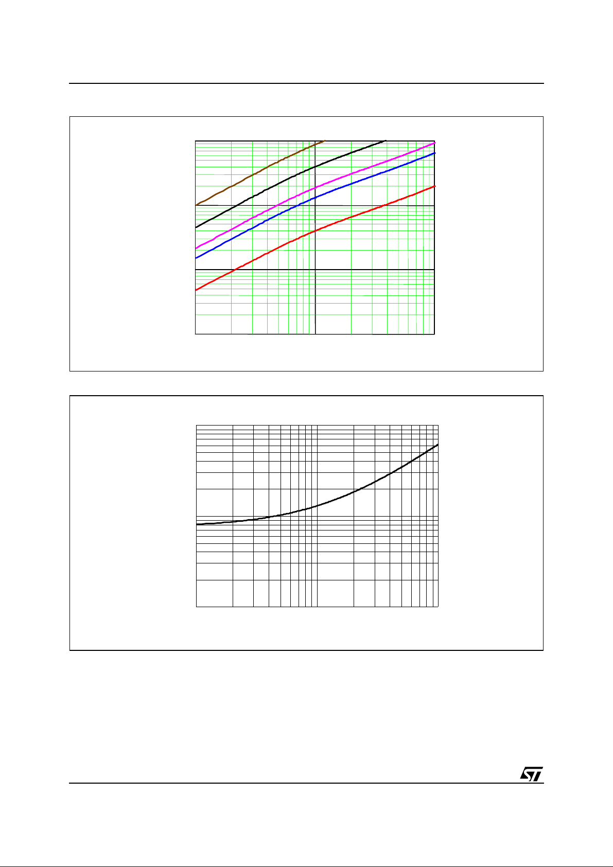
Thermal Management
In most applications the power dissipation in the IC is the main factor that sets the maximum current that can
be delivered by the devic e in a safe operating condi tion. Therefore, it has to be taken into account very carefully.
Besides the available space on the P CB, the right package s hould be chosen c onsidering the power dissi pation.
Heat sinking can be achieved using copper on the PCB with proper area and thickness. Figures 28, 29 and 30
show the Junction-to-Ambient Thermal Resistance values for the PowerSO36, PowerDIP24 and SO24 packages.
For instance, using a PowerSO package with copper slug soldered on a 1.5mm copper thickness FR4 board
with 6cm
2
dissipating footprint (copper thick ness of 35µm), the R
th(j-a mb )
is about 35°C/W. Fig. 31 shows mounting methods for this package. Using a multi- layer board wi th vias to a ground plane, thermal impeda nce can be
reduced down to 15°C/W.
21/27

L6208
Figure 28. PowerSO36 Junction-Ambient Thermal Resistance versus On-Board Copper Area.
ºC / W
43
38
33
28
23
18
13
12345678910111213
Without Ground Layer
With Ground Layer
With Ground Layer+16 via
Holes
sq. cm
On-Board Copper Area
Figure 29. PowerDIP24 Junction-Ambi ent Therm al Resis tance vers us On -B oard Copp er Area.
ºC / W
49
48
47
46
45
44
43
42
41
40
39
1 2 3 4 5 6 7 8 9 101112
Copper Area is on Bottom
Side
Copper Area is on Top Side
sq. cm
On-Board Copper Area
Figure 30. SO24 Junction-Ambient Thermal Resistance versus On-Board Copper Area.
ºC / W
68
66
64
62
60
58
56
54
52
50
48
123456789101112
Copper Area is on Top Side
sq. cm
On-Board Copper Area
Figure 31. Mounting the PowerSO Packag e.
Slug soldered
to PCB with
dissipati ng area
Slug soldered
to PCB with
dissipating area
plus ground layer
Slug soldered to PCB with
dissipa t ing area plus ground lay e r
contacted through via holes
22/27
L6208
Figure 32. Typical Quiescent Current vs.
Supply Voltage
Iq [mA ]
5.6
5.4
fsw = 1kHz Tj = 25°C
Tj = 85°C
Tj = 125°C
5.2
5.0
4.8
4.6
0 102030405060
[V]
V
S
Figure 33. Normalized Typical Quiescen t
Current vs. Switching Frequency
Iq / (Iq @ 1 kHz)
1.7
1.6
1.5
1.4
1.3
1.2
1.1
1.0
0.9
0 20406080100
[kHz]
f
SW
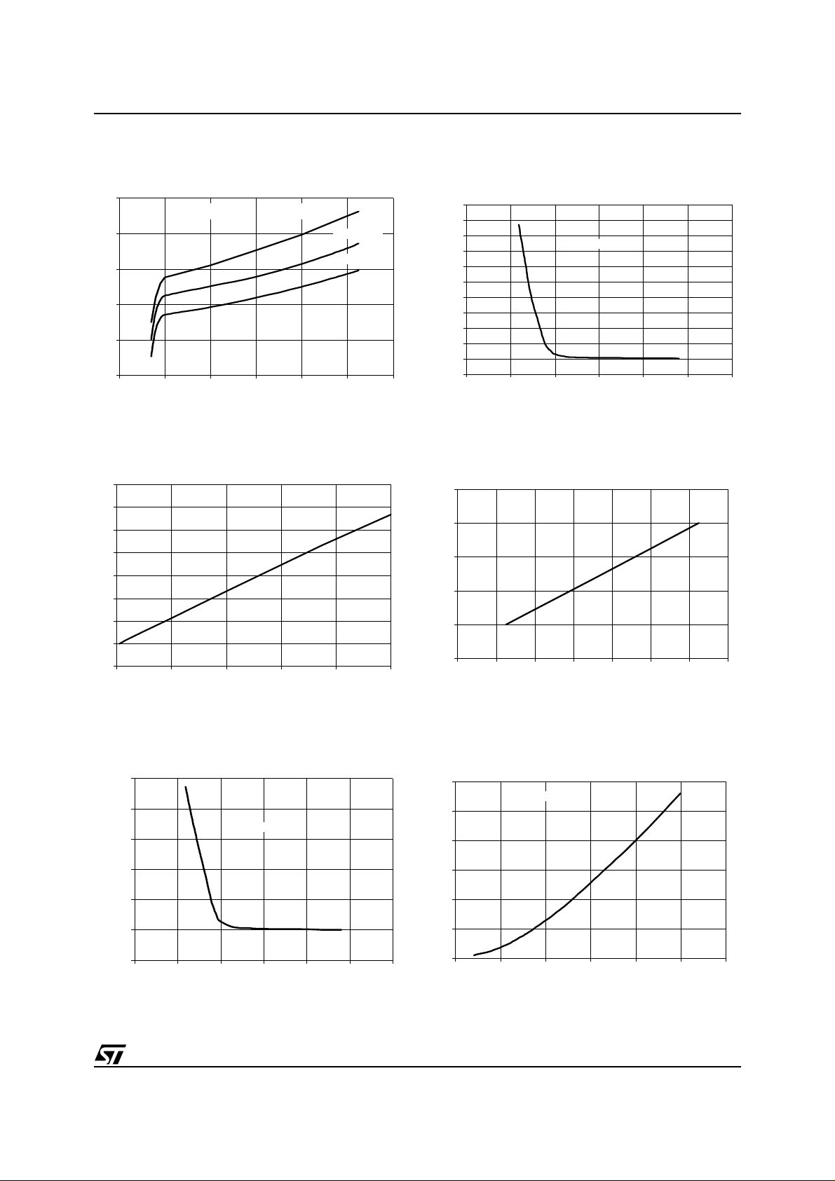
Figure 35. Ty pi c al Hi gh-Side RDS ( ON ) v s.
Supply Voltage
R
[Ω]
DS(ON)
0.380
0.376
0.372
0.368
0.364
0.360
0.356
0.352
0.348
0.344
0.340
0.336
0 5 10 15 20 25 30
Figure 36. Nor m ali ze d R
Tj = 25°C
[V]
V
S
DS(ON)
vs.Junction
Temperature (typical value)
/ (R
R
DS(ON)
1.8
1.6
1.4
1.2
1.0
0.8
0 20406080100120140
DS(ON)
@ 25 °C)
Tj [°C]
Figure 34. Typical Low-Side R
DS(ON)
Voltage
[Ω]
R
DS(ON)
0.300
0.296
Tj = 25°C
0.292
0.288
0.284
0.280
0.276
0 5 10 15 20 25 30
V
[V]
S
vs. Supply
Figure 37. Typical Drain-Source Diode Forward
ON Characteristic
I
[A]
SD
3.0
2.5
2.0
1.5
1.0
0.5
0.0
700 800 900 1000 1100 1200 1300
Tj = 25°C
V
[mV]
SD
23/27

L6208
DIM.
MIN. TYP. MAX. MIN. TYP. MAX.
mm inch
A 3.60 0.141
a1 0.10 0.30 0.004 0.012
a2 3.30 0.130
a3 0 0.10 0 0.004
b 0.22 0.38 0.008 0.015
c 0.23 0.32 0.009 0.012
D (1) 15.80 16.00 0.622 0.630
D1 9.40 9.80 0.370 0.385
E 13.90 14.50 0.547 0.570
e 0.65 0.0256
e3 11.05 0.435
E1 (1) 10.90 11.10 0.429 0.437
E2 2.90 0.114
E3 5.80 6.20 0.228 0.244
E4 2.90 3.20 0.114 0.126
G 0 0.10 0 0.004
H 15.50 15.90 0.610 0.626
h 1.10 0.043
L 0.80 1.10 0.031 0.043
N10°(max.)
S8°(max.)
(1): "D" and "E1" do not include mold flash or protrusions
- Mold flash or protrusions shall not exceed 0.15mm (0.006 inch)
- Critical dimensions are "a3", "E" and "G".
OUTLINE AND
MECHANICAL DATA
PowerSO36
NN
a2
A
1936
0.12 AB
⊕
e
M
E1
DETAIL B
lead
a3
B
Gage Plane
PSO36MEC
BOTTOM VIEW
DETAIL B
0.35
S
E
DETAIL A
L
E2
h x 45˚
DETAIL A
118
A
e3
H
D
b
c
a1
slug
E3
D1
- C -
SEATING PLANE
GC
(COPLANARITY)
24/27

L6208
DIM.
MIN. TYP. MAX. MIN. TYP. MAX.
A 4.320 0.170
A1 0.380 0.015
A2 3.300 0.130
B 0.410 0.460 0.510 0.016 0.018 0.020
B1 1.400 1.520 1.650 0.055 0.060 0.065
c 0.200 0.250 0.300 0.008 0.010 0.012
D 31.62 31.75 31.88 1.245 1.250 1.255
E 7.620 8.260 0.300 0.325
e 2.54 0.100
E1 6.350 6.600 6.860 0.250 0.260 0.270
e1 7.620
L 3.180 3.430 0.125 0.135
M 0˚ min, 15˚ max.
mm inch
0.300
OUTLINE AND
MECHANICAL DATA
Powerdip 24
E1
A2
A
13
12
A1
SDIP24L
e1
c
M
L
B eB1
D
24
1
25/27

L6208
DIM.
MIN. TYP. MAX. MIN. TYP. MAX.
A 2.35 2.65 0.093 0.104
A1 0 .10 0.30 0.004 0.012
B 0.33 0.51 0.013 0.200
C 0.23 0.32 0.009 0.013
(1)
15.20 15.60 0.598 0.614
D
E 7.40 7.60 0.291 0.299
e 1.2 7 0.050
H 10.0 10.65 0.394 0.419
h 0.25 0;75 0.010 0.030
L 0.40 1.27 0.016 0.050
k 0˚ (min.), 8˚ (max.)
ddd 0.10 0.0 04
(1) “ D” dime nsion does not include m ol d flash, protusi on s or gate
burrs. Mo ld f las h, p rotus ion s or g at e bur rs sh all not exce ed
0.15mm per side.
mm inch
OUTLINE AND
MECHANICAL DA TA
Weight: 0.60gr
SO24
Information furnished is believed to be accurate and reliable. However, STMicroelectronics assumes no responsibility for the consequences
of use of such information nor for any infringement of patents or other rights of third parties which may result from its use. No license is granted
by implic ation or o therwise under any patent or p atent right s of STMicroelectronics. Specificat ions ment i oned in th i s publicati on are subj ect
to change without notice. This publication supersedes and replaces all information previously supplied. STMicroelectronics product s are not
authoriz ed for use as critical comp onents in life support devices or systems without express wri tten appr oval of STMicroelectronics.
The ST logo is a registered trademark of STMicroelectr oni cs.
All other names are the propert y of their respective owners
© 2003 STMi croelectro nics - All right s reserve d
Australi a - Belgium - Brazil - Canada - China - C zech Republi c - Finlan d - F rance - Germany - Hong Kon g - India - Israel - Italy - Japan -
Malaysia - Malta - Morocco - Singapore - Spain - Sweden - Switzerland - United Kingdom - United States
STMicroelectronics GROUP OF COMPANIES
www.st.com
0070769 C
26/27

L6208
Information furnished is believed to be accurate and reliable. However, STMicroelectronics assumes no responsibility for the consequences
of use of such information nor for any infringement of patents or other rights of third parties which may result from its use. No license is granted
by implic ation or o therwise under any patent or p atent right s of STMicroelectronics. Specificat ions ment i oned in th i s publicati on are subj ect
to change without notice. This publication supersedes and replaces all information previously supplied. STMicroelectronics product s are not
authoriz ed for use as critical comp onents in life support devices or systems without express wri tten appr oval of STMicroelectronics.
The ST logo is a registered trademark of STMicroelectr oni cs.
All other names are the propert y of their respective owners
© 2003 STMi croelectro nics - All right s reserve d
Australi a - Belgium - Brazil - Canada - China - C zech Republi c - Finlan d - F rance - Germany - Hong Kon g - India - Israel - Italy - Japan -
Malaysia - Malta - Morocco - Singapore - Spain - Sweden - Switzerland - United Kingdom - United States
STMicroelectronics GROUP OF COMPANIES
www.st.com
27/27
 Loading...