

Page 1
DMOS DUAL FULL BRIDGE DRIVER
WITH PWM CURRENT CONTROLLER
■
OPERATING SUPPLY VOLTAGE FROM 8 TO 52V
■ 5.6A OUTPUT PEAK CURRENT (2.8A DC)
■ R
■ OPERATING FREQUENCY UP TO 100KHz
■ NON DISSIPATIVE OVERCURRENT
PROTECTION
■ DUAL INDEPENDENT CONSTANT t
CURRENT CONTROLLERS
■ SLOW DECAY SYNCHRONOUS
RECTIFICATION
■ CROSS CONDUCTION PROTECTION
■ THERMAL SHUTDOWN
■ UNDER VOLTAGE LOCKOUT
■
INTEGRATED FAST FREE WHEELING DIODES
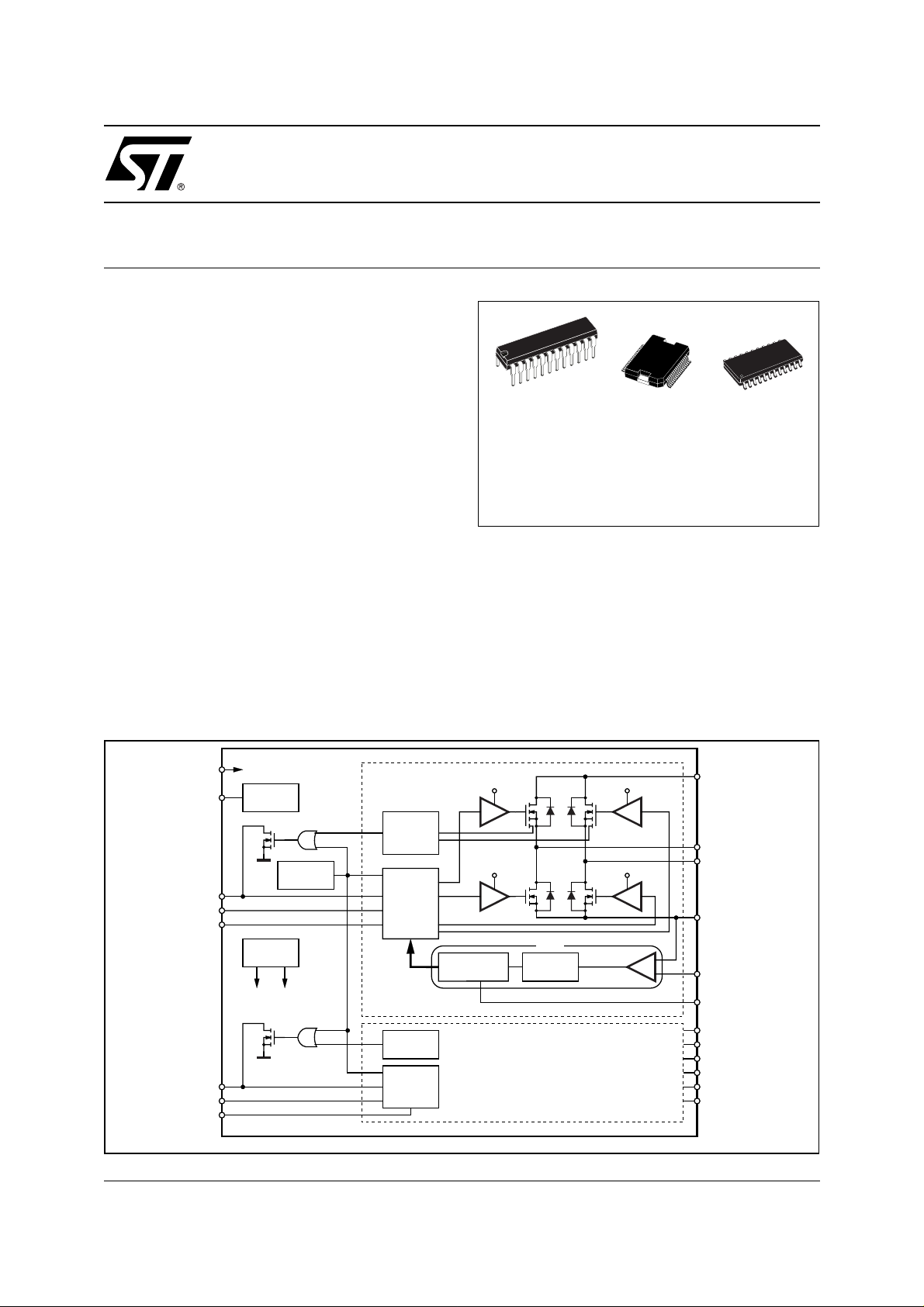
TYPICAL APPLICATIONS
■ BIPOLAR STEPPER MOTOR
■ DUAL DC MOTOR
DESCRIPTION
The L6207 is a DMOS Dual Full Bridge designed for
motor control applications, realized in MultiPower-
BLOCK DIAGRAM
0.3Ω TYP. VA LUE @ Tj = 25 °C
DS(ON)
OFF
PWM
L6207
PowerDIP24
(20+2+2)
BCD technology, which combines isolated DMOS
Power Transistors with CMOS and bipolar circuits on
the same chip. The device al so includes two independent constant off time PWM Current Controllers
that performs the chopping regulation. Available in
PowerDIP24 (20+2+2), PowerSO36 and SO24
(20+2+2) packages, the L6207 features a non-di ssi pative overcurrent protection on the high side Power
MOSFETs and thermal shutdown.
PowerSO36
ORDERING NUMBERS:
L6207N (PowerDIP24)
L6207PD (PowerSO36)
L6207D (SO24)
SO24
(20+2+2)
VBOOT
September 2003
VCP
EN
IN1
IN2
EN
IN1
IN2
V
BOOT
CHARGE
PUMP
OCD
A
THERMAL
PROTECTION
A
A
A
VOLTAGE
REGULATOR
5V10V
OCD
B
B
B
B
OVER
CURRENT
DETECTION
GATE
LOGIC
OVER
CURRENT
DETECTION
GATE
LOGIC
V
BOOT
10V 10V
ONE SHOT
MONOSTABLE
MASKING
PWM
TIME
V
BOOT
SENSE
COMPARATOR
BRIDGE A
BRIDGE B
+
-
D99IN1085A
VS
A
OUT1
OUT2
SENSE
VREF
RC
A
V
S
B
OUT1
OUT2
SENSE
VREF
RC
B
A
A
A
A
B
B
B
B
1/23
Page 2

L6207
ABSOLUTE MAXIMUM RATINGS
Symbol Parameter Test conditions Value Unit
V
S
V
OD
V
BOOT
V
IN,VEN
V
REFA
V
REFB
V
RCA, VRCB
V
SENSEA,
V
SENSEB
I
S(peak)
I
S
, T
T
stg
Supply Voltage
Differential Voltage between
VSA, OUT1A, OUT2A, SENSEA and
VSB, OUT1B, OUT2B, SENSE
Bootstrap Peak Voltage
VSA =
VSB = V
VSA =
VSB = VS = 60V;
V
SENSEA
B
VSA =
VSB = V
= V
S
SENSEB
S
= GND
60 V
60 V
VS + 10 V
Input and Enable Voltage Range -0.3 to +7 V
,
Voltage Range at pins V
and V
REFB
REFA
Voltage Range at pins RCA and
RC
B
Voltage Range at pins SENSEA
and SENSE
B
Pulsed Supply Current (for each
pin), internally limited by the
V
S
VSA =
t
PULSE
VSB = VS;
< 1ms
-0.3 to +7 V
-0.3 to +7 V
-1 to +4 V
7.1 A
overcurrent protection
RMS Supply Current (for each
pin)
V
S
Storage and Operating
OP
VSA =
VSB = V
S
2.8 A
-40 to 150 °C
Temperature Range
RECOMMENDED OPERATING CONDITIONS
Symbol Parameter Test Conditions MIN MAX Unit
V
V
OD
V
REFA
V
REFB
V
SENSEA,
V
SENSEB
I
OUT
T
f
sw
Supply Voltage
S
Differential Voltage Between
VSA, OUT1A, OUT2A, SENSEA and
VSB, OUT1B, OUT2B, SENSE
,
Voltage Range at pins V
and V
REFB
Voltage Range at pins SENSEA
and SENSE
B
REFA
VSA =
VSA =
V
SENSEA
B
(pulsed tW < trr)
(DC)
VSB = V
VSB = VS;
= V
SENSEB
S
852V
-0.1 5 V
-6
-1
RMS Output Current 2.8 A
Operating Junction Temperature -25 +125 °C
j
Switching Frequency 100 KHz
52 V
6
1
V
V
2/23
Page 3
L6207
THERMA L D ATA
Symbol Description PowerDIP24 SO24 PowerSO36 Unit
R
th-j-pins
R
th-j-case
R
th-j-amb1
R
th-j-amb1
R
th-j-amb1
R
th-j-amb2
(1) Mounted on a multi-layer FR4 PCB with a dissipati ng copper surface on the bottom side of 6cm2 (with a thickness of 35µm).
(2) Mounted on a multi-layer FR4 PCB with a dissipati ng copper surface on the top side of 6cm2 (with a thickness of 35µm).
(3) Mounted on a multi-layer FR4 PCB with a dissipating copper surface on the top side of 6cm2 (with a thickness of 35µm), 16 via holes
and a groun d l ayer.
(4) Mounted on a multi-layer FR4 PCB without any hea t s i nking surfac e on the board.
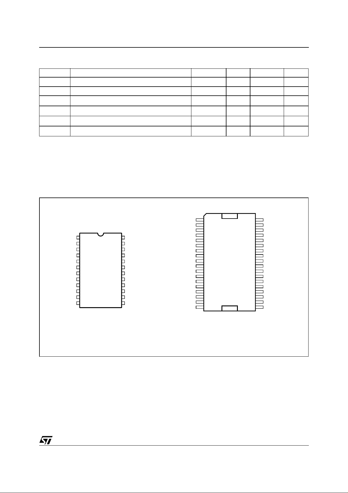
PIN CONNECTIONS (Top View)
Maximum Thermal Resistance Junction-Pins 18 14 - °C/W
Maximum Thermal Resistance Junction-Case - - 1 °C/W
Maximum Thermal Resistance Junction-Ambient
Maximum Thermal Resistance Junction-Ambient
Maximum Thermal Resistance Junction-Ambient
Maximum Thermal Resistance Junction-Ambient
1
2
3
4
43 51 - °C/W
--35°C/W
--15°C/W
58 77 62 °C/W
IN1
IN2
SENSE
RC
OUT1
GND
GND
OUT1
RC
SENSE
IN1
IN2
1
A
2
A
3
A
4
A
5
A
6
7
8
B
9
B
10
B
11
B
12
B
D02IN1346
VREF
24
23
22
21
20
EN
VCP
OUT2
VS
A
A
A
A
GND19
GND
18
VS
17
B
OUT2
16
15
14
13
VBOOT
EN
B
VREF
B
B
PowerDIP24 /SO2 4
(5) The slug is internally connected to pins 1,18,19 and 36 (GND pins).
GND
N.C.
N.C.
VS
OUT2
N.C. N.C.
VCP
EN
VREF
IN1
IN2
SENSE
RC
N.C.
OUT1
N.C.
N.C. N.C.
GND GND
1
2
3
4
A
5
A
6
7
8
A
9
A
10 27
A
11
A
12
A
13 24
A
14
15
A
16
17
18
D02IN1347
PowerSO36
36
35
34
33
32
31
30
29
28
26
25
23
22
21
20
19
(5)
GND
N.C.
N.C.
VS
B
OUT2
VBOOT
EN
B
VREF
IN2
B
IN1
B
SENSE
RC
B
N.C.
OUT1
N.C.
B
B
B
B
3/23
Page 4

L6207
PIN DESCRIPTION
P ACKAGE
SO24/
PowerDIP24
PowerSO36
Name T ype Function
PIN # PIN #
1 10 IN1
2 11 IN2
3 12 SENSE
413RC
5 15 OUT1
6, 7,
18, 19
1, 18,
19, 36
GND GND Signal Ground terminals. In Power DIP and SO packages,
8 22 OUT1
924RC
10 25 SENSE
11 26 IN1
12 27 IN2
13 28 VREF
14 29 EN
A
A
Logic input Bridge A Logic Input 1.
Logic input Bridge A Logic Input 2.
Power Supply Bridge A Source Pin. This pin must be connected to Power
A
Ground through a sensing power resistor.
A
RC Pin RC Network Pin. A parallel RC network connected
between this pin and ground sets the Current Controller
OFF-Time of the Bridge A.
Power Output Bridge A Output 1.
A
these pins are also used for heat dissipation toward the
PCB.
Power Output Bridge B Output 1.
B
B
RC Pin RC Network Pin. A parallel RC network connected
between this pin and ground sets the Current Controller
OFF-Time of the Bridge B.
Power Supply Bridge B Source Pin. This pin must be connected to Power
B
Ground through a sensing power resistor.
B
B
Logic Input Bridge B Input 1
Logic Input Bridge B Input 2
Analog Input Bridge B Current Controller Reference Voltage.
B
Do not leave this pin open or connect to GND.
(6)
B
Logic Input
Bridge B Enable. LOW logic level switches OFF all Power
MOSFETs of Bridge B. This pin is also connected to the
collector of the Overcurrent and Thermal Protection
transistor to implement over current protection.
If not used, it has to be connected to +5V through a
resistor.
15 30 VBOOT Supply
Voltage
16 32 OUT2
17 33 VS
Power Output Bridge B Output 2.
B
Power Supply Bridge B Power Supply Voltage. It must be connected to
B
Bootstrap Voltage needed for driving the upper Power
MOSFETs of both Bridge A and Bridge B.
the supply voltage together with pin VS
20 4 VS
Power Supply Bridge A Power Supply Voltage. It must be connected to
A
the supply voltage together with pin VS
21 5 OUT2
Power Output Bridge A Output 2.
A
22 7 VCP Output Charge Pump Oscillator Output.
4/23
.
A
.
B
Page 5

L6207
PIN DESCRIPTION
23 8 EN
(continued)
A
Logic Input
(6)
Bridge A Enable. LOW logic level switches OFF all Power
MOSFETs of Bridge A. This pin is also connected to the
collector of the Overcurrent and Thermal Protection
transistor to implement over current protection.
If not used, it has to be connected to +5V through a
resistor.
24 9 VREF
Analog Input Bridge A Current Controller Reference Voltage.
A
Do not leave this pin open or connect to GND.
(6) Al so connec te d at the ou tput drain of the Over current and Thermal protecti on MOSFET . Therefore, it has to be driven putting in
series a re si stor with a v al ue in the ran ge of 2.2KΩ - 180KΩ, recomme nded 100KΩ.
ELECTRICAL CHARACTERISTICS
(T
= 25 °C, Vs = 48V, unless otherwise specified)
amb
Symbol Parameter Test Conditions Min Typ Max Unit
V
Sth(ON)
V
Sth(OFF)
T
j(OFF)
Output DMOS Transistors
Turn-on Threshold 6.6 7 7.4 V
Turn-off Threshold 5.6 6 6.4 V
I
Quiescent Supply Current All Bridges OFF;
S
T
j
= -25°C to 125°C
(7)
510mA
Thermal Shutdown Temperature 165 °C
R
DS(ON)
High-Side Switch ON Resistance Tj = 25 °C 0.34 0.4 Ω
Low-Side Switch ON Resistance T
I
DSS
Leakage Current EN = Low; OUT = V
Source Drain Diodes
V
Forward ON Voltage ISD = 2.8A, EN = LOW 1.15 1.3 V
SD
t
Reverse Recovery Time If = 2.8A 300 ns
rr
t
Forward Recovery Time 200 ns
fr
Logic Input
V
V
V
th(ON)
V
th(OFF)
V
th(HYS)
Low level logic input voltage -0.3 0.8 V
IL
High level logic input voltage 2 7 V
IH
I
Low Level Logic Input Current GND Logic Input Voltage -10 µA
IL
I
High Level Logic Input Current 7V Logic Input Voltage 10 µA
IH
Turn-on Input Threshold 1.8 2.0 V
Turn-off Input Threshold 0.8 1.3 V
Input Threshold Hysteresis 0.25 0.5 V
T
=125 °C
j
= 25 °C 0.28 0.34 Ω
j
=125 °C
T
j
(7)
(7)
S
0.53 0.59 Ω
0.47 0.53 Ω
2mA
EN = Low; OUT = GND -0.15 mA
5/23
Page 6

L6207
ELECTRICAL CHARACTERISTICS (continued)
(T
= 25 °C, Vs = 48V, unless otherwise specified)
amb
Symbol Parameter Test Conditions Min Typ Max Unit
Switching Characteristics
(8)
I
t
D(on)EN
t
D(on)IN
t
RISE
t
D(off)EN
t
D(off)IN
t
FALL
f
Enable to out turn ON delay time
Input to out turn ON delay time
Output rise time
(8)
Enable to out turn OFF delay time
Input to out turn OFF delay time
Output Fall Time
Dead Time Protection 0.5 1 µs
t
dt
CP
Charge pump frequency
(8)
PWM Comparator and Monostable
(8)
=2.8A, Resistive Load 100 250 400 ns
LOAD
I
=2.8A, Resistive Load
LOAD
1.6 µs
(dead time included)
I
=2.8A, Resistive Load 40 250 ns
LOAD
I
=2.8A, Resistive Load 300 550 800 ns
LOAD
I
=2.8A, Resistive Load 600 ns
LOAD
I
=2.8A, Resistive Load 40 250 ns
LOAD
-25°C<Tj <125°C 0.6 1 MHz
I
RCA, IRCB
V
offset
Source Current at pins RCA and
RC
B
Offset Voltage on Sense
V
= V
RCA
V
REFA, VREFB
= 2.5V 3.5 5.5 mA
RCB
= 0.5V ±5 mV
Comparator
t
PROP
t
BLANK
Turn OFF Propagation Delay
Internal Blanking Time on
(9)
SENSE pins
t
ON(MIN)
t
OFF
I
BIAS
Minimum On Time 1.5 2 µs
PWM Recirculation Time R
R
OFF
OFF
= 20KΩ; C
= 100KΩ; C
OFF
OFF
= 1nF
= 1nF
Input Bias Current at pins VREFA
and VREFB
Over Current Protection
I
SOVER
R
OPDR
t
OCD(ON)
t
OCD(OFF)
(7) Tested at 25°C in a restricted range and guaranteed by characterization.
(8) See Fig. 1.
(9) Measured applying a voltage of 1V to pin SEN S E and a voltag e drop from 2V to 0V to pin VREF.
(10) See Fig. 2.
Input Supply Overcurrent
Protection Threshold
= -25°C to 125°C
T
j
Open Drain ON Resistance I = 4mA 40 60 Ω
OCD Turn-on Delay Time (10) I = 4mA; CEN < 100pF 200 ns
OCD Turn-off Delay Time (10) I = 4mA; CEN < 100pF 100 ns
(7)
4 5.6 7.1 A
500 ns
1µs
13
61
µs
µs
10 µA
6/23
Page 7
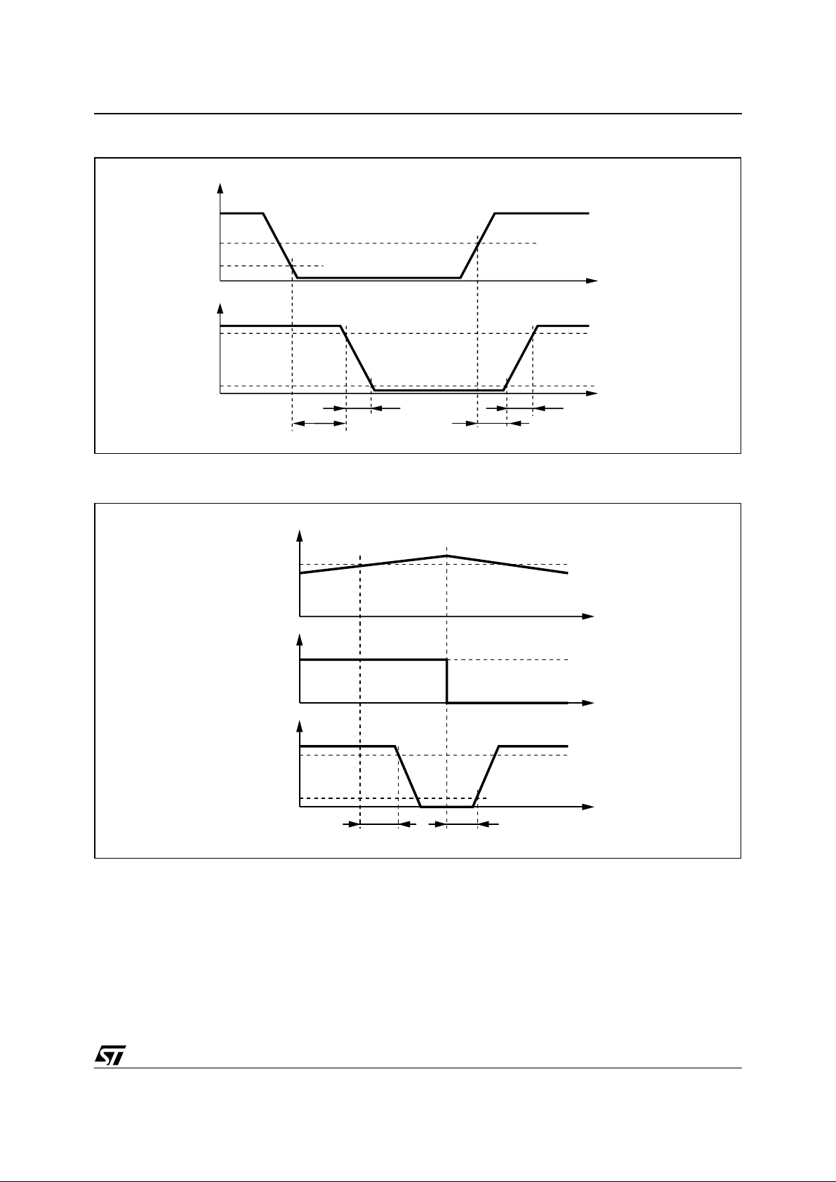
Figure 1. Switching Characteristic Definition
EN
V
th(ON)
V
th(OFF)
I
OUT
90%
10%
D01IN1316
t
D(OFF)EN
t
FALL
Figure 2. Ove rcurrent Detect i on Timi ng Definition
t
D(ON)EN
t
RISE
L6207
t
t
I
OUT
I
SOVER
ON
BRIDGE
OFF
V
EN
90%
10%
t
OCD(ON)
t
OCD(OFF)
D02IN1399
7/23
Page 8

L6207
9
0
CIRCUIT DESCRIPTION
POWER STAGES and CHARGE PUMP
The L6207 integrates two independent Power MOS
Full Bridges. Each Power MOS has an Rdson =
0.3ohm (typical value @ 25°C), with intrinsic fast
freewheeling diode. Cross conduction protection is
achieved using a dead time (td = 1
tween the switch off and switch on of two P ower MOS
in one leg of a bridge.
Using N Channel Power MOS for the upper transistors in the bridge requires a gate drive voltage above
the power supply voltage. The Bootstrapped
(VBOOT) supply is obtained through an internal Oscillator and few external components to realize a
charge pump circuit as shown in Figure 3. The oscillator output (VCP) is a square wave at 600kHz (typical) with 10V amplitude. Recommended values/part
numbers for the charge pump circuit are shown in
Table1.
µ
s typical) be-
thermal protection MOSFETs (one for the Bridge A
and one for the Bridge B) are also connected to these
pins. Due to these connections some care needs to
be taken in driving these pins. The EN
and ENB in-
A
puts may be driven in one of two configurati ons as
shown in figures 5 or 6. If driven by an open drain
(collector) structure, a pull-up resistor R
pacitor C
are connected as shown in Fig. 5. I f t he
EN
and a ca-
EN
driver is a standard Push-Pull str ucture the resist or
R
and the capacitor CEN are connected as shown
EN
in Fig. 6. The resistor R
range from 2.2k
for R
and CEN are respectively 100KΩ and 5.6nF.
EN
Ω
to 180KΩ. Recommended values
should be chosen i n the
EN
More information on selecting the values is found in
the Overcurrent Protection section.
Figure 4. Logi c Inp ut s I nte rn a l St ructure
Table 1. Charge Pump External Components
Values
C
BOOT
C
P
R
P
D1 1N4148
D2 1N4148
220nF
10nF
100Ω
Figure 3. Char ge Pump Circu it
V
S
D1
D2
R
P
C
P
VCP VBOOT VS
C
BOOT
VS
B
D01IN1328
A
LOGIC INPUTS
Pins IN1A, IN2B, IN1B and IN2B are TTL/CMOS and
uC compatible logic inputs. The internal structure is
shown in Fig. 4. Typical value for turn-on and turn-off
thresholds are respectively Vthon = 1.8V and Vthoff
= 1.3V.
Pins EN
and ENB have identical input structure with
A
the exception that the drains of the Overcurrent and
Figure 5. EN
Driving
OPEN
COLLECTOR
OUTPUT
Figure 6. EN
PUSH-PULL
OUTPUT
5V
ESD
PROTECTION
D01IN1329
and ENB Pins Open Collector
A
5V
R
EN
ENA or EN
and ENB Pins Push-Pull Driving
A
R
EN
C
EN
ENA or EN
B
B
C
EN
5V
D02IN134
5V
D02IN135
8/23
Page 9

L6207
TRUTH TABLE
INPUTS OUTPUTS
EN IN1 IN2 OUT1 OUT2
L X X High Z High Z Disable
H L L GND GND Brake Mode (Lower Path)
H H L Vs GND (Vs) Forward
H L H GND (Vs) Vs Reverse
H H H Vs Vs Brake Mode (Upper Path)
X = Don't care
High Z = High Impedance Output
GND (Vs) = GND during Ton, Vs during Toff
(*) Valid only in case of load connected between OUT1 and OUT2
PWM CURRENT CONTROL
The L6207 includes a constant off time PWM current controller for each of the two bridges. The current control
circuit senses the bridge current by sensing the voltage drop across an external sense resistor connected between the source of the two lower power MOS transistors and ground, as shown in Figure 7. As the current in
the load builds up the voltage across the sense resistor increases proportionally. When the voltage drop across
the sense resistor becomes greater than the voltage at the reference input (VREF
parator triggers the monostable switching the low-side MOS off. The low-side MOS remain off for the time set
by the monostable and the motor current recirculates in the upper path. When the monostable times out the
bridge will again turn on. Since t he i nternal dead ti me, us ed to prev ent c ross c onduction i n the bridge, delays
the turn on of the power MOS, the effective off time is the sum of the monostable time plus the dead time.
Description (*)
or VREFB) the sense com-
A
Figure 7. PWM Current Controller Simplified Schematic
VS
(or B)
A
S
R
BLANKING TIME
MONOSTABLE
MONOSTABLE
RESET
1µs
BLANKER
SENSE
COMPARATOR
COMPARATOR
OUTPUT
GATE DRIVERS
DRIVERS
+
DEAD TIME
+
-
VREF
FROM THE
LOW-SIDE
A(or B)
2H 1H
DRIVERS
+
DEAD TIME
2L 1L
SENSE
R
SENSE
A(or B)
OUT2
OUT1
I
OUT
A(or B)
A(or B)
D02IN1352
LOAD
(or B)
A
5mA
5V
C
TO GATE LOGIC
(0) (1)
RC
R
Q
-
+
2.5V
A(or B)
Figure 8 shows the typical operating waveforms of the output current, the voltage drop acr oss the sensing resistor, the RC pin voltage and the status of the bridge. Immediately aft er the l ow-side Power MOS turns on, a
high peak current flows through the sensing resistor due to the reverse recovery of the freewheeling diodes. The
L6207 provides a 1
µ
s Blanking Time t
that inhibits the comparator output so that this current spike cannot
BLANK
prematurely re-trigger the monostable.
9/23
Page 10

L6207
Figure 8. Output Current Regulation Waveforms
I
OUT
V
REF
R
SENSE
V
SENSE
V
REF
0
V
RC
5V
2.5V
ON
OFF
SYNCHRONOUS RECTIFICATION
D02IN1351
t
OFF
1µs t
BLANK
t
ON
Slow Decay Slow Decay
t
RCRISE
t
RCFALL
1µs t
DT
BC
DDA
t
BC
t
OFF
1µs t
t
RCRISE
RCFALL
1µs t
BLANK
DT
Figure 9 shows the magnitude of the Off T ime t
culated from the equations:
t
t
where R
20K
0.47nF ≤ C
t
= 0.6 · R
RCFALL
= t
OFF
RCFALL
and C
OFF
Ω ≤
= 1µs (typical value)
DT
R
OFF
OFF
OFF
· C
OFF
+ tDT = 0.6 · R
OFF
· C
OFF
OFF
+ t
are the external component values and tDT is the internally generated Dead Time with:
≤ 100K
Ω
≤ 100nF
Therefore:
t
OFF(MIN)
t
OFF(MAX)
These values allow a sufficient range of t
The capacitor value chosen for C
Rise Time t
= 6.6µs
= 6ms
to implement the drive circuit for most motors.
OFF
also affects the Rise Time t
will only be an i ssue if the capacitor i s not completely charged before the next time the
RCRISE
OFF
monostable is triggered. Therefore, t he on time t
10/23
versus C
OFF
DT
, which depends by motors and supply parameters, has to
ON
OFF
and R
RCRISE
values. It can be approximately cal-
OFF
of the voltage at the pin RCOFF. The
Page 11

L6207
be bigger than t
can not be smaller than the minimum on time t
t
>1.5µs (typ. value)=
ONtON MIN()
t
ONtRCRISEtDT
RCRISE
= 600 · C
t
for allowing a good current regulation by the PWM stage. Furthermore, the on time t
RCRISE
ON(MIN)
.
–>
OFF
ON
Figure 10 shows the lower limit for the on time tON for having a good PWM current regulation capacity. It has to
be said that t
than t
RCRISE
So, small C
switching frequency), but, the smaller is the value for C
is always bigger than t
ON
ON(MIN)
- tDT. In this last case the device continues to work but the off time t
value gives more f lexibilit y for t he applic ations (allows smaller on ti me and, t herefore, higher
OFF
because the device imposes this condition, but it can be smaller
is not more constant.
OFF
, the more influential will be the noises on the circuit
OFF
performance.
Figure 9. t
versus C
OFF
OFF
1.10
1.10
and R
4
3
OFF
= 100kΩ
R
off
= 47kΩ
R
off
= 20k
R
100
toff [µs]
10
1
0.1 1 10 100
Ω
off
Coff [nF]
11/23
Page 12

L6207
Figure 10. Area where tON can vary maintaining the PWM regulation.
100
10
ton(min) [µs]
1.5µs (typ. value)
1
0.1 1 10 100
Coff [nF]
SLOW DECAY MODE
Figure 11 shows the operation of the bridge in the Slow Decay mode. At the start of the off time, the lower power
MOS is switched off and the current recirculates around the upper half of the bridge. Since the voltage across
the coil is low, the current decays slowly. After the dead time the upper power MOS is operated in the synchronous rectification mode. When the monostable times out, the lower power MOS is turned on again after some
delay set by the dead time to prevent cross conduction.
Figure 11. Slow Decay Mode Output Stage Configurations
A) ON TIME B) 1µs DEAD TIME C) SYNCHRONOUS
D01IN1336
RECTIFICATION
D) 1µs DEAD TIME
12/23
Page 13

L6207
NON-DISSIPATIVE OVERCURRENT PROTECTION
The L6207 integrates an Overcurrent Detecti on Circui t (OCD). This cir cuit provides protection agai nst a short
circuit to ground or between two phases of the bridge. With this internal over current detection, the external current sense resistor normally used and its associated power dissipation are eliminated. Figure 12 shows a simplified schematic of the overcurrent detection circuit.
To implement the over current detection, a sensing element that delivers a small but precise fraction of the output current is implemented with each high side power MOS. Since this current is a small fraction of the output
current there is very little additional power dissipation. This current is compared with an internal reference current I
OCD comparator signals a fault condition. When a fault condition is detected, the EN pin is pulled below the turn
off threshold (1.3V typical) by an internal open drain MOS with a pull down capability of 4mA. By using an external R-C on the EN pin, the off time before recovering normal operation can be easily programmed by means
of the accurate thresholds of the logic inputs.
Figure 12. Overcurrent Protection Simplified Schematic
. When the output current in one bridge reaches the detection threshold (typically 5.6A) the relat ive
REF
OUT2
VS
OUT1
µC or LOGIC
+5V
RENEN
C
EN
A
TO GATE
R
DS(ON)
40Ω TYP.
LOGIC
INTERNAL
OPEN-DRAIN
POWER SENSE
1 cell
OCD
COMPARATOR
A
I
POWER DMOS
n cells
I
/ n
1A
(I1A+I2A) / n
I
REF
OVER TEMPERATURE
1A I2A
A
+
A
POWER DMOS
n cells
I
/ n
2A
HIGH SIDE DMOSs OF
THE BRIDGE A
POWER SENSE
1 cell
D02IN1353
Figure 13 shows the Overcurrent Detection operation. The Disable Time t
DISABLE
before recovering normal operation can be easily programmed by means of the accurate thresholds of the logic inputs. It is affected whether by
C
and REN values and its magnitude is reported in Figure 14. The Delay Time t
EN
bridge when an overcurrent has been detected depends only by C
value. Its magnitude is reported in Figure 15.
EN
CEN is also used for providing immunity to pin EN against fast transient noises. Therefore the value of C
before turning off the
DELAY
EN
should be chosen as big as possible according to the maximum tolerable Delay Time and the REN value should
be chosen according to the desired Disable Time.
The resistor R
should be chosen in the range from 2.2KΩ to 180KΩ. Recommended values for REN and C
EN
EN
are respectively 100KΩ and 5.6nF that allow obtaining 200µs Disable Time.
13/23
Page 14

L6207
Figure 13. Overcurrent Protection Wavefo rms
I
OUT
I
SOVER
V
EN
V
DD
V
th(ON)
V
th(OFF)
ON
OCD
OFF
V
EN(LOW)
ON
BRIDGE
OFF
t
OCD(ON)
t
DELAY
t
EN(FALL)
t
D(OFF)EN
t
OCD(OFF)
t
DISABLE
t
EN(RISE)
t
D(ON)EN
D02IN1400
14/23
Page 15

L6207
Figure 14. t
Figure 15. t
DISABLE
versus C
DELAY
versus CEN and R
3
3
1.10
1.10
100
100
[µs]
[µs]
DISABLE
DISABLE
t
t
10
10
1
1
1 10 100
1 10 100
EN (VDD
= 5V).
EN (VDD
= 5V).
REN= 220 k
REN= 220 k
Ω
Ω
CEN[n F]
CEN[nF]
REN= 100 k
REN= 100 k
Ω
Ω
R
R
R
R
R
R
EN
EN
EN
EN
EN
EN
= 47 k
= 47 k
= 33 k
= 33 k
= 10 k
= 10 k
Ω
Ω
Ω
Ω
Ω
Ω
10
s]
µ
1
tdelay [
0.1
1 10 100
Cen [nF]
THERMAL PROTECTION
In addition to the Ovecurrent Protection, the L6207 int egrates a Thermal Protection for preventing t he device
destruction in case of junction over temperature. It works sensing the die temperature by means of a sensible
element integrated in the die. The device switch-off when the junction temperature reaches 165°C (typ. value)
with 15°C hysteresis (typ. value).
15/23
Page 16

L6207
APPLICATION INFORMATION
A typical application using L6207 is shown in Fig. 16. Typical component values for the application are shown
in Table 3. A high quality ceramic capacitor in the range of 100 to 200 nF should be placed between the power
pins (VS
reduce high frequency transients generated by the switching. The capacitors connected from the EN
inputs to ground set the shut down time for the BrgidgeA and BridgeB respectively when an over current is detected (see Overcurrent Protection). The two current sensing inputs (SENSE
ed to the sensing resistors with a trace length as short as possible in the layout. The sense resistors should be
non-inductive resistors to minimize the di/dt transients across the resistor. To increase noise immunity, unused
logic pins (except EN
pin description). It is recommended to keep Power G round and Signal Ground separated on PCB.
Table 2. Component Values for Typical Application
C
C
C
C
C
C
C
C
C
C
and VSB) and ground near the L6207 to improve the high frequency filtering on the power supply and
A
and SENSEB) should be connect-
A
and ENB) are best connected to 5V (High Logic Level) or GND (Low Logic Level) (see
A
1
2
A
B
BOOT
P
ENA
ENB
REFA
REFB
100uF D
100nF D
1nF R
1nF R
220nF R
10nF R
5.6nF R
5.6nF R
68nF R
68nF
1
2
A
B
ENA
ENB
P
SENSEA
SENSEB
1N4148
1N4148
39KΩ
39KΩ
100KΩ
100KΩ
100Ω
0.3Ω
0.3Ω
and EN
A
B
Figure 16. Typical Application
+
VS
8-52V
DC
POWER
GROUND
-
SIGNAL
GROUND
C
1
C
2
D
1
C
BOOT
R
SENSEA
R
SENSEB
LOAD
LOAD
VS
A
20
B
17
R
VCP
P
C
D
2
VBOOT
SENSE
SENSE
OUT1
A
OUT2
B
OUT1
OUT2
P
GND
GND
GND
GND
22
15
A
3
B
10
A
5
A
21
B
8
B
16
18
19
6
7
24VS
13
23
14
11
12
1
2
4
9
D02IN1343
VREF
VREF
EN
EN
IN1
IN2
IN1
IN2
RC
RC
A
B
C
REFA
A
B
C
ENA
B
B
A
A
C
A
A
R
A
C
B
B
R
B
IN1
IN2
IN1
IN2
C
REFB
R
R
C
B
B
A
A
ENA
ENB
ENB
V
V
REFA
REFB
EN
EN
= 0-1V
= 0-1V
A
B
16/23
Page 17

L6207
OUTPUT CURRENT CAPABILITY AND IC POWER DISSIPATION
In Fig. 17 and Fig. 18 are shown the approximate relation between the output current and the IC power dissipation using PWM current control driving two loads, for two different driving types:
– One Full Bridge ON at a time (Fig.17) in which only one load at a time is energized.
– Two Full Bridges ON at the same time (Fig.18) in which two loads at the same time are energized.
For a given output current and driving type the power dissipated by the IC can be easily evaluated, in order to
establish which package should be used and how large must be the on-board copper dissipating area to guarantee a safe operating junction temperature (125°C maximum).
Figure 17. IC Power Dissipation versus Output Curr ent with One Full Bridge ON at a time.
ONE FULL BRIDGE ON AT A TIME
10
I
A
I
OUT
8
6
PD [W]
4
I
B
I
OUT
Test Conditions:
2
Supply Voltage = 24V
No PWM
0
0 0.5 1 1.5 2 2.5 3
I
[A]
OUT
f
= 30 kHz (slow decay)
SW
Figure 18. IC Power Dissipation versus Output Current with Two Full Bridges ON at the same time.
TWO FULL BRIDGES ON AT THE SAME TIME
10
8
6
PD [W]
4
2
0
00.511.522.53
I
[A]
OUT
I
A
I
B
I
OUT
I
OUT
Test Conditions:
Supply Voltage = 24V
No PWM
= 30 kHz (slow decay)
f
SW
THERMAL MANAGEMENT
In most applications the power dissipation in the IC is the main factor that sets the maximum cur rent that can be delivered by the device in a safe operating condition. Therefore, it has to be taken into account very carefully. Besides
the available space on the P CB , the right package should be c hosen considering the power dissipation. H eat sinking
can be achieved using cop per on th e PC B w ith proper area and thickness. Figures 20, 21 a nd 22 s how th e Junc tionto-Ambient Thermal Resistance values for the PowerSO36, PowerDIP24 and SO 24 packages.
For instance, using a PowerSO package with copper slug soldered on a 1.5 mm copper thickness FR4 board
with 6cm
2
dissipating footprint (copper thickness of 35µm), the R
is about 35°C/W. Fig. 19 shows mount-
th j-a mb
ing methods for this package. Using a multi-layer board with vias to a ground plane, thermal impedance can be
reduced down to 15°C/W.
17/23
Page 18

L6207
Figure 19. Mounting the PowerSO pack age.
Slug soldered
to PCB with
dissipating area
Slug soldered
to PCB with
dissipating area
plus ground layer
Slug soldered to PCB with
dissipating area plus ground layer
contacted through via holes
Figure 20. PowerSO36 Junction -Am bient thermal resi stance versus on-bo ard co pper area.
ºC / W
43
38
33
28
23
18
13
12345678910111213
Without Ground Layer
With Ground Layer
With Ground Layer+16 via
Holes
sq. cm
On-Board Copper Area
Figure 21. PowerDIP24 Junction-Ambient thermal resistance versus on-board copper area.
ºC / W
49
48
47
46
45
44
43
42
41
40
39
1 2 3 4 5 6 7 8 9 101112
Copper Area is on Bottom
Side
Copper Area is on Top Side
sq . cm
On-Board Copper Area
Figure 22. SO24 Junction-Ambient thermal resi stance versus on-bo ard copp er area.
18/23
ºC / W
68
66
64
62
60
58
56
54
52
50
48
123456789101112
Copper Area is on Top Side
sq. cm
On-Board Copper Area
Page 19

L6207
Figure 23. Typical Quiescent Current vs.
Supply Voltage
Iq [mA ]
5.6
5.4
fsw = 1kHz Tj = 25°C
Tj = 85°C
Tj = 125°C
5.2
5.0
4.8
4.6
0 102030405060
[V]
V
S
Figure 24. Normalized Typical Quiescen t
Current vs. Switching Frequency
Iq / (Iq @ 1 kHz)
1.7
1.6
1.5
1.4
1.3
1.2
1.1
1.0
0.9
0 20406080100
[kHz]
f
SW
Figure 26. Typical Hi gh-Side RDS(ON) vs.
Supply Voltage
R
[Ω]
DS(ON)
0.380
0.376
0.372
0.368
0.364
0.360
0.356
0.352
0.348
0.344
0.340
0.336
0 5 10 15 20 25 30
Figure 27. Normalized R
Tj = 25°C
[V]
V
S
DS(ON)
vs.Junction
Temperature (typical value)
/ (R
R
DS(ON)
1.8
1.6
1.4
1.2
1.0
0.8
0 20406080100120140
DS(ON)
@ 25 °C)
Tj [°C]
Figure 25. Ty pi cal Lo w- S i de R
DS(ON)
Supply Voltage
[Ω]
R
DS(ON)
0.300
0.296
Tj = 25°C
0.292
0.288
0.284
0.280
0.276
0 5 10 15 20 25 30
V
[V]
S
vs.
Figure 28. Typical Drain-Source Diode
Forward ON Characteristic
I
[A]
SD
3.0
2.5
2.0
1.5
1.0
0.5
0.0
700 800 900 1000 1100 1200 1300
Tj = 25°C
V
[mV]
SD
19/23
Page 20

L6207
DIM.
MIN. TYP. MAX. MIN. TYP. MAX.
mm inch
A 3.60 0 .141
a1 0.10 0.30 0.004 0.012
a2 3.30 0.130
a3 0 0.10 0 0.004
b 0.22 0.38 0.008 0.015
c 0.23 0.32 0.009 0.012
D (1) 15.80 16.00 0.622 0.630
D1 9.40 9.80 0.370 0.385
E 13.90 14.50 0.547 0.570
e 0.65 0.0256
e3 11.05 0.435
E1 (1) 10.90 11.10 0.429 0.437
E2 2.90 0.114
E3 5.80 6.20 0.228 0.244
E4 2.90 3.20 0.114 0.126
G 0 0.10 0 0.004
H 15.50 15.90 0.610 0.626
h 1.10 0.043
L 0.80 1.10 0.031 0.043
N10°(max.)
S8°(max.)
(1): "D" and "E1" do not include mold flash or protrusions
- Mold flash or protrusions shall not exceed 0.15mm (0.006 inch)
- Critical dimensions are "a3", "E" and "G".
OUTLINE AND
MECHANICAL DATA
PowerSO36
E2
NN
a2
A
1936
0.12 AB
⊕
e
M
E1
DETAIL B
lead
a3
B
Gage Plane
PSO36MEC
BOTTOM VIEW
DETAIL B
0.35
S
E
DETAIL A
slug
L
(COPLANARITY)
h x 45˚
DETAIL A
118
A
e3
H
D
b
c
a1
E3
D1
- C -
SEATING PLANE
GC
20/23
Page 21

L6207
DIM.
MIN. TYP. MAX. MIN. TYP. MAX.
A 4.320 0.170
A1 0.380 0.015
A2 3.300 0.130
B 0.410 0.460 0.510 0.016 0.018 0.020
B1 1.400 1.520 1.650 0.055 0.060 0.065
c 0.200 0.250 0.300 0.008 0.010 0.012
D 31.62 31.75 31.88 1.245 1.250 1.255
E 7.620 8.260 0.300 0.325
e 2.54 0.100
E1 6.350 6.600 6.860 0.250 0.260 0.270
e1 7.620
L 3.180 3.430 0.125 0.135
M 0˚ min, 15˚ max.
mm inch
0.300
OUTLINE AND
MECHANICAL DATA
Powerdip 24
E1
A2
A
13
12
A1
SDIP24L
e1
c
M
L
B eB1
D
24
1
21/23
Page 22

L6207
DIM.
MIN. TYP. MAX. MIN. TY P. MA X.
A 2.35 2.65 0.093 0.104
A1 0 .10 0.30 0.004 0.012
B 0.33 0.51 0.013 0.200
C 0.23 0.32 0.009 0.0 13
(1)
15.20 15.60 0.598 0.614
D
E 7.40 7.60 0.291 0.299
e 1.27 0.050
H 10.0 10.65 0.394 0.419
h 0.25 0;75 0.010 0.030
L 0.40 1.27 0.016 0.050
k 0˚ (min.), 8˚ (max.)
ddd 0.10 0.004
(1) “ D” dimension does not include mol d flas h, prot u s ions or gate
burrs. Mo ld f las h, p rotus ion s or g at e bur rs sh all not exce ed
0.15mm per side.
mm inch
OUTLINE AND
MECHANICAL DA TA
Weight: 0.60gr
SO24
22/23
0070769 C
Page 23

L6207
Information furnished is believed to be accurate and reliable. However, STMicroelectronics assumes no responsibility for the consequences
of use of such information nor for any infringement of patents or other rights of third parties which may result from its use. No license is granted
by implic ation or o therwise under any patent or p atent right s of STMicroelectronics. Specificat ions ment i oned in th i s publicati on are subj ect
to change without notice. This publication supersedes and replaces all information previously supplied. STMicroelectronics product s are not
authoriz ed for use as critical comp onents in life support devices or systems without express wri tten appr oval of STMicroelectronics.
The ST logo is a registered trademark of STMicroelectr oni cs.
All other names are the propert y of their respective owners
© 2003 STMi croelectro nics - All right s reserve d
Australi a - Belgium - Brazil - Canada - China - C zech Republi c - Finlan d - F rance - Germany - Hong Kon g - India - Israel - Italy - Japan -
Malaysia - Malta - Morocco - Singapore - Spain - Sweden - Switzerland - United Kingdom - United States
STMicroelectronics GROUP OF COMPANIES
www.st.com
23/23
 Loading...