

Features
■ Operating supply voltage from 8 to 52 V
■ 5.6 A output peak current
■ R
0.3 Ω typ. value @ TJ = 25 °C
DS(on)
■ Operating frequency up to 100 kHz
■ Programmable high side overcurrent detection
and protection
■ Diagnostic output
■ Paralleled operation
■ Cross conduction protection
■ Thermal shutdown
■ Undervoltage lockout
■ Integrated fast free wheeling diodes
Application
■ Bipolar stepper motor
■ Dual or quad DC motor
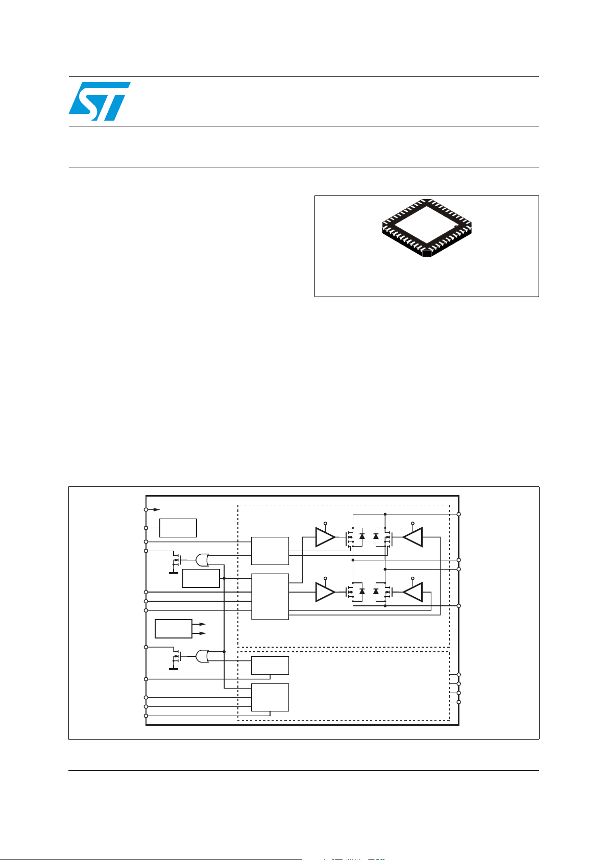
Figure 1. Block diagram
L6206Q
DMOS dual full bridge driver
QFN-48
(7 x 7 mm)
Description
The L6206Q is a DMOS dual full bridge designed
for motor control applications, developed using
BCDmultipower technology, which combines
isolated DMOS power transistors with CMOS and
bipolar circuits on the same chip. Available in
QFN48 7x7 package, the L6206Q features
thermal shutdown and a non-dissipative
overcurrent detection on the high side power
MOSFETs plus a diagnostic output that can be
easily used to implement the overcurrent
protection.
VBOOT
VCP
PROGCL
OCD
EN
IN1
IN2
OCD
PROGCL
EN
IN1
IN2
A
A
A
A
A
B
B
B
B
B
V
BOOT
CHARGE
PUMP
VOLTAGE
REGULATOR
OCD
THERMAL
PROTECTION
OCD
10V
5V
VS
V
BOOT
OVER
A
B
CURRENT
DETECTION
GATE
LOGIC
OVER
CURRENT
DETECTION
GATE
LOGIC
V
BOOT
V01V01
BRIDGE A
BRIDGE B
A
OUT1
OUT2
SENSE
V
S
B
OUT1
OUT2
SENSE
A
A
A
B
B
B
AM02555v1
November 2011 Doc ID 022028 Rev 1 1/30
www.st.com
30

Contents L6206Q
Contents
1 Electrical data . . . . . . . . . . . . . . . . . . . . . . . . . . . . . . . . . . . . . . . . . . . . . . 3
1.1 Absolute maximum ratings . . . . . . . . . . . . . . . . . . . . . . . . . . . . . . . . . . . . . 3
1.2 Recommended operating conditions . . . . . . . . . . . . . . . . . . . . . . . . . . . . . 3
2 Pin connection . . . . . . . . . . . . . . . . . . . . . . . . . . . . . . . . . . . . . . . . . . . . . . 4
3 Electrical characteristics . . . . . . . . . . . . . . . . . . . . . . . . . . . . . . . . . . . . . 6
4 Circuit description . . . . . . . . . . . . . . . . . . . . . . . . . . . . . . . . . . . . . . . . . . . 9
4.1 Power stages and charge pump . . . . . . . . . . . . . . . . . . . . . . . . . . . . . . . . . 9
4.2 Logic inputs . . . . . . . . . . . . . . . . . . . . . . . . . . . . . . . . . . . . . . . . . . . . . . . . 9
4.3 Non-dissipative overcurrent detection and protection . . . . . . . . . . . . . . . 11
4.4 Thermal protection . . . . . . . . . . . . . . . . . . . . . . . . . . . . . . . . . . . . . . . . . . 15
5 Application information . . . . . . . . . . . . . . . . . . . . . . . . . . . . . . . . . . . . . 16
6 Paralleled operation . . . . . . . . . . . . . . . . . . . . . . . . . . . . . . . . . . . . . . . . 18
7 Output current capability and IC power dissipation . . . . . . . . . . . . . . 22
8 Thermal management . . . . . . . . . . . . . . . . . . . . . . . . . . . . . . . . . . . . . . . 23
9 Electrical characteristics curves . . . . . . . . . . . . . . . . . . . . . . . . . . . . . . 24
10 Package mechanical data . . . . . . . . . . . . . . . . . . . . . . . . . . . . . . . . . . . . 26
11 Order codes . . . . . . . . . . . . . . . . . . . . . . . . . . . . . . . . . . . . . . . . . . . . . . . 28
12 Revision history . . . . . . . . . . . . . . . . . . . . . . . . . . . . . . . . . . . . . . . . . . . 29
2/30 Doc ID 022028 Rev 1

L6206Q Electrical data
1 Electrical data
1.1 Absolute maximum ratings
Table 1. Absolute maximum ratings
Symbol Parameter Parameter Value Unit
V
Supply voltage VSA = VSB = VS 60 V
S
V
OD
OCD
OCDB
Differential voltage between VSA,
OUT1A, OUT2A, SENSEA and VSB,
, OUT2B, SENSE
OUT1
B
,
A
OCD pins voltage range -0.3 to +10 V
B
VSA = VSB = VS = 60V;
VSENSEA = VSENSEB =
GND
60 V
PROGCL
PROGCLB
V
V
V
SENSEA
V
SENSEB
I
S(peak)
,
A
PROGCL pins voltage range -0.3 to +7 V
BOOT
IN,VEN
Bootstrap peak voltage VSA = VSB = VS V
Input and enable voltage range -0.3 to +7 V
,
Voltage range at pins SENSEA and
SENSE
Pulsed supply current (for each VS
pin), internally limited by the
overcurrent protection
B
= VSB = VS;
V
SA
t
PULSE
IS RMS supply current (for each VS pin) VSA = VSB = VS 2.5 A
T
, TOP
stg
Storage and operating temperature
range
1.2 Recommended operating conditions
Table 2. Recommended operating conditions
Symbol Parameter Parameter Min. Max. Unit
Supply voltage VSA = VSB = VS 8 52 V
V
S
Differential voltage between VSA,
V
OUT1A, OUT2A, SENSEA and VSB,
OD
OUT1B, OUT2B, SENSEB
= VSB = VS;
VS
A
V
SENSEA
< 1ms
= V
SENSEB
+ 10 V
S
-1 to +4 V
7.1 A
-40 to 150 °C
52 V
,
V
SENSEA
V
SENSEB
I
OUT
T
f
sw
Voltage range at pins SENSEA and
SENSEB
RMS output current 2.5 A
Operating junction temperature -25 +125 °C
j
Switching frequency 100 kHz
Pulsed t
DC -1 1 V
< t
W
rr
-6 6 V
Doc ID 022028 Rev 1 3/30
Pin connection L6206Q
2 Pin connection
Figure 2. Pin connection (top view)
OUT1A
OUT1A
GND
OUT1B
OUT1B
NC
SENSEA
OCDA
48 47 46 45 44 43 42 41 40 39 38 37
1
NC
EPAD
2
3
4
NC
5
NC
6
7
NC
8
NC
9
NC
10
11
12
NC
13 14 15 16 17 18 19 20 21 22 23 24
NC
OCDB
SENSEB
SENSEA
SENSEB
IN2A
IN1B
IN1A
IN2B
Note: The exposed PAD must be connected to GND pin.
Table 3. Pin description
ENA
PROGCLA
ENB
PROGCLB
VCPNCOUT2A
OUT2A
OUT2B
OUT2B
VBOOT
36
NC
35
VSA
34
VSA
33
NC
32
NC
31
GND
30
NC
29
NC
28
NC
27
VSB
26
VSB
25
NC
NC
AM02556v1
Pin Name Type Function
43 IN1A Logic input Bridge A logic input 1.
44 IN2A Logic input Bridge A logic input 2.
45, 46 SENSEA Power supply
Bridge A source pin. This pin must be connected to power ground
directly or through a sensing power resistor.
Bridge A overcurrent detection and thermal protection pin. An internal
48 OCDA Open-drain output
open-drain transistor pulls to GND when overcurrent on bridge A is
detected or in case of thermal protection.
2, 3 OUT1A Power output Bridge A output 1.
6, 31 GND GND
Signal ground terminals. These pins are also used for heat dissipation
toward the PCB.
10, 11 OUT1B Power output Bridge B output 1.
Bridge B overcurrent detection and thermal protection pin. An internal
13 OCDB Open-drain output
open-drain transistor pulls to GND when overcurrent on bridge B is
detected or in case of thermal protection.
15, 16 SENSEB Power supply
Bridge B source pin. This pin must be connected to power ground
directly or through a sensing power resistor.
4/30 Doc ID 022028 Rev 1

L6206Q Pin connection
Table 3. Pin description (continued)
Pin Name Type Function
17 IN1B Logic input Bridge B input 1
18 IN2B Logic input Bridge B input 2
Bridge B overcurrent level programming. A resistor connected between
19 PROGCLB R pin
20 ENB Logic input
21 VBOOT Supply voltage
22, 23 OUT2B Power output Bridge B output 2.
26, 27 VSB Power supply
this pin and ground sets the programmable current limiting value for
bridge B. By connecting this pin to ground the maximum current is set.
This pin cannot be left unconnected.
Bridge B enable. LOW logic level switches OFF all power MOSFETs of
bridge B. If not used, it must be connected to +5 V.
Bootstrap voltage needed for driving the upper power MOSFETs of both
bridge A and bridge B.
Bridge B power supply voltage. It must be connected to the supply
voltage together with pin VSA.
34, 35 VSA Power supply
38, 39 OUT2A Power output Bridge A output 2.
40 VCP Output Charge pump oscillator output.
41 ENA Logic input
42 PROGCLA R pin
Bridge A power supply voltage. It must be connected to the supply
voltage together with pin VSB.
Bridge A enable. LOW logic level switches OFF all power MOSFETs of
bridge A. If not used, it must be connected to +5 V.
Bridge A overcurrent level programming. A resistor connected between
this pin and ground sets the programmable current limiting value for
bridge A. By connecting this pin to ground, the maximum current is set.
This pin cannot be left unconnected.
Doc ID 022028 Rev 1 5/30

Electrical characteristics L6206Q
3 Electrical characteristics
VS = 48 V, TA = 25 °C, unless otherwise specified.
Table 4. Electrical characteristics
Symbol Parameter Test condition Min. Typ. Max. Unit
V
Sth(ON)
V
Sth(OFF)
IS Quiescent supply current
T
j(OFF)
Turn-on threshold 6.6 7 7.4 V
Turn-off threshold 5.6 6 6.4 V
All bridges OFF; Tj = -25 °C to
125 °C
(1)
510mA
Thermal shutdown temperature 165 °C
Output DMOS transistors
Tj = 25 °C 0.34 0.4
R
DS(ON)
I
DSS
High-side switch ON resistance
Tj =125 °C
Tj = 25 °C 0.28 0.34
Low-side switch ON resistance
Tj =125 °C
EN = Low; OUT = V
Leakage current
EN = Low; OUT = GND -0.15 mA
(1)
(1)
0.53 0.59
0.47 0.53
2mA
S
Source drain diodes
V
Forward ON voltage ISD = 2.5 A, EN = LOW 1.15 1.3 V
SD
t
rr
t
fr
Reverse recovery time If = 2.5 A 300 ns
Forward recovery time 200 ns
Logic input
Ω
V
V
I
I
V
th(ON)
V
th(OFF)
V
th(HYS)
IH
IL
IH
Low level logic input voltage -0.3 0.8 V
IL
High level logic input voltage 2 7 V
Low level logic input current GND logic input voltage -10 µA
High level logic input current 7 V logic input voltage 10 µA
Turn-on input threshold 1.8 2 V
Turn-off input threshold 0.8 1.3 V
Input threshold hysteresis 0.25 0.5 V
Switching characteristics
t
D(on)EN
t
D(on)IN
t
RISE
Enable pin to out, turn ON delay time
(2)
Input pin to out, turn ON delay time
Output rise time
(2)
=2.5 A, resistive load 100 250 400 ns
I
LOAD
=2.5 A, resistive load (dead
I
LOAD
time included)
I
=2.5 A, resistive load 40 250 ns
LOAD
6/30 Doc ID 022028 Rev 1
1.6 µs
L6206Q Electrical characteristics
Table 4. Electrical characteristics (continued)
Symbol Parameter Test condition Min. Typ. Max. Unit
t
D(off)EN
t
D(off)IN
t
FAL L
t
dt
f
CP
Enable pin to out, turn OFF delay
(2)
time
Input pin to out, turn OFF delay time I
Output fall time
(2)
I
I
=2.5 A, resistive load 300 550 800 ns
LOAD
=2.5 A, resistive load 600 ns
LOAD
=2.5 A, resistive load 40 250 ns
LOAD
Dead time protection 0.5 1 µs
Charge pump frequency -25 °C<Tj <125 °C 0.6 1 MHz
Overcurrent detection
I
s over
Input supply overcurrent detection
threshold
-25 °C<Tj <125 °C; RCL= 39 kΩ
-25 °C<Tj <125 °C; RCL= 5 kΩ
-25 °C<Tj <125 °C; RCL= GND
0.57
4.42
5.6
ROPDR Open-drain ON resistance I = 4 mA 40 60 Ω
t
OCD(ON)
t
OCD(OFF)
1. Tested at 25 °C in a restricted range and guaranteed by characterization.
2. See Figure 3.
3. See Figure 4.
OCD turn-on delay time
OCD turn-off delay time
(3)
I = 4 mA; CEN < 100 pF 200 ns
(3)
I = 4 mA; CEN < 100 pF 100 ns
Figure 3. Switching characteristic definition
EN
A
A
A
V
V
th(OFF)
I
th(ON)
OUT
90%
10%
D01IN1316
t
D(OFF)EN
t
FAL L
t
D(ON)EN
t
RISE
t
t
AM02557v1
Doc ID 022028 Rev 1 7/30
Electrical characteristics L6206Q
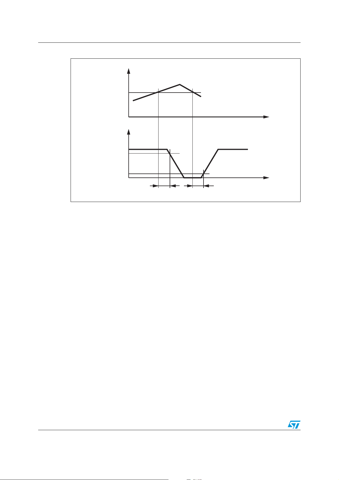
Figure 4. Overcurrent detection timing definition
I
OUT
OCD
Threshold
t
V
OCD
90%
10%
t
t
OCD(ON)
t
OCD(OFF)
AM02558v1
8/30 Doc ID 022028 Rev 1
L6206Q Circuit description
4 Circuit description
4.1 Power stages and charge pump
The L6206Q integrates two independent Power MOS full bridges. Each power MOS has an
R
conduction protection is implemented by using a dead time (t
an internal timing circuit between the turn-off and turn-on of two power MOSFETs in one leg
of a bridge.
= 0.3 Ω (typical value @ 25 °C) with intrinsic fast freewheeling diode. Cross
DS(ON)
= 1 µs typical value) set by
DT
Pins VS
and VSB must be connected together to the supply voltage (VS).
A
Using an N-channel power MOSFET for the upper transistors in the bridge requires a gate
drive voltage above the power supply voltage. The bootstrapped supply (V
) is obtained
BOOT
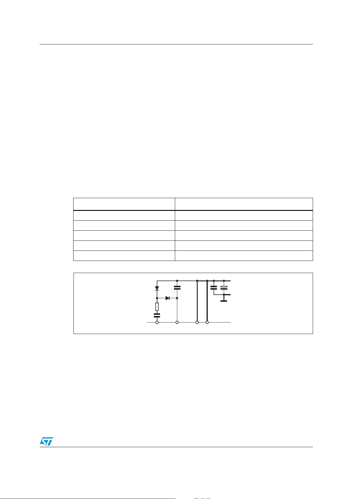
through an internal oscillator and few external components to realize a charge pump circuit,
as shown in Figure 5. The oscillator output (pin VCP) is a square wave at 600 kHz (typically)
with 10 V amplitude. Recommended values/part numbers for the charge pump circuit are
shown in Ta bl e 5 .
Table 5. Charge pump external component values
Component Value
C
BOOT
C
P
R
P
220 nF
10 nF
100 Ω
D1 1N4148
D2 1N4148
Figure 5. Charge pump circuit
V
S
D1
R
C
VCP VBOOT VS
C
D2
P
P
BOOT
VS
A
B
AM02559v1
4.2 Logic inputs
Pins IN1A, IN2A, IN1B, IN2B, ENA, and ENB are TTL/CMOS and µC compatible logic inputs.
The internal structure is shown in Figure 6. The typical values for turn-on and turn-off
thresholds are respectively V
Pins EN
connecting them respectively to the outputs OCD
outputs. If this type of connection is chosen, particular care needs to be taken in driving
these pins. Two configurations are shown in Figure 7 and Figure 8. If driven by an open-
drain (collector) structure, a pull-up resistor R
and ENB are commonly used to implement overcurrent and thermal protection by
A
=1.8 V and V
thon
= 1.3 V.
thoff
and OCDB, which are open-drain
A
and a capacitor CEN are connected as
EN
Doc ID 022028 Rev 1 9/30
 Loading...