

Page 1
DMOS DUAL FULL BRIDGE DRIVER
■
SUPPLY VOLTAGE UP TO 48V
■
R
■
CROSS CONDUCTION PROTECTION
■
THERMAL SHUTDOWN
■
0.5A DC CURRENT
■
TTL/CMOS COMPATIBLE DRIVER
■
HIGH EFFICIENCY CHOPPING
■
MULTIPOWER BCD TECHNOLOGY
DESCRIPTION
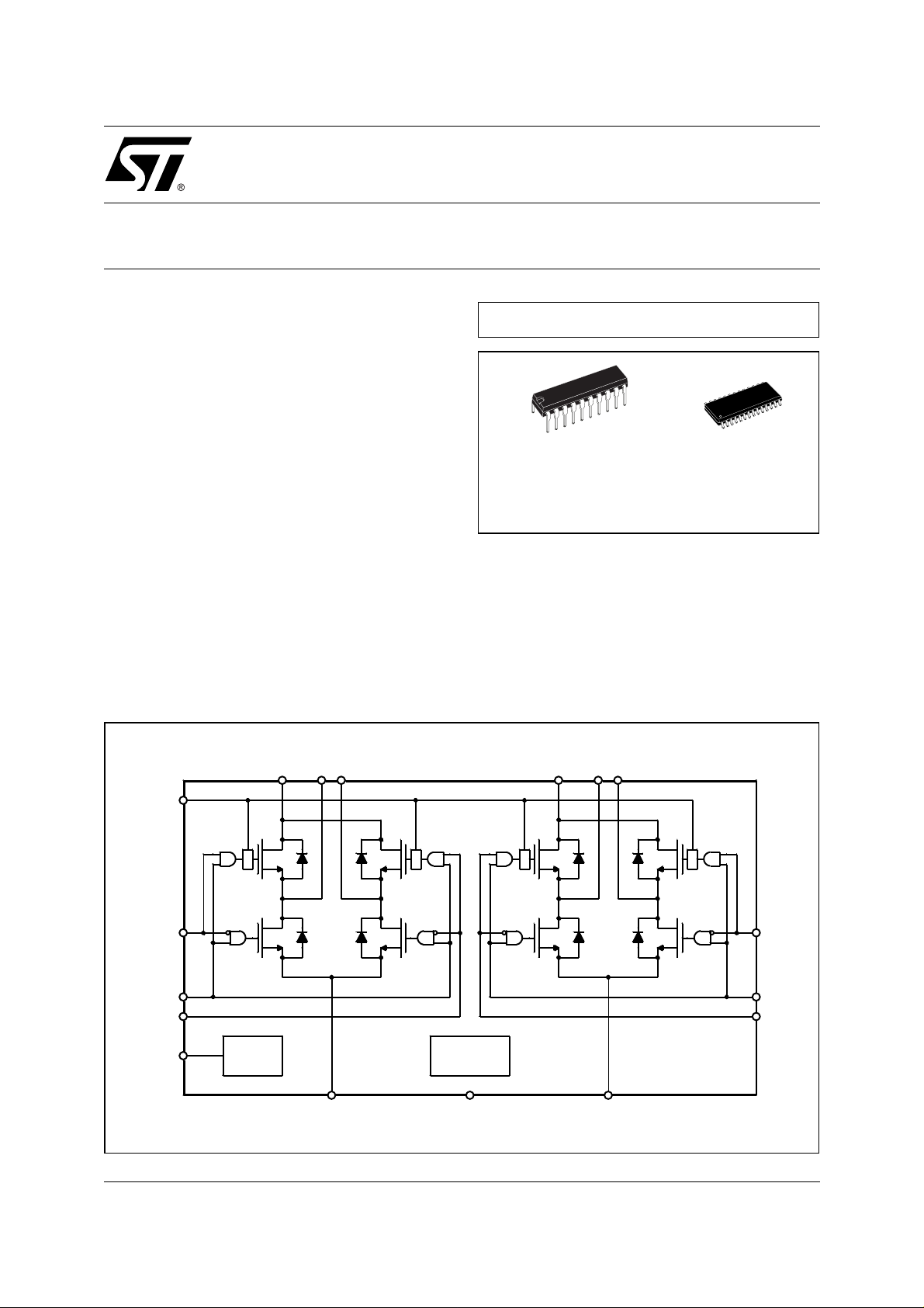
The L6204 is a dual full bridge driver for motor
control applications realized in BCD technology
which combines isolated DMOS power transistors
with CMOS and Bipolar circuits on the same chip.
By using mixed technology it has been possible to
optimize the logic circuitry and the powe r stage to
achieve the best possible performance.
The logic inputs are TTL/CMOS compatible. Both
channels are controlled by a separate Enable.
1.2Ω L6204 (25°C)
DS(ON)
L6204
MULTOPOWER BCD TECHNOLOGY
Powerdip 16+2+2 SO 24+2+2
ORDERING NUMBERS:
L6204 L6204D
Each bridge has a sense resistor to control the
currenrt lev e l.
The L6204 is mounted in an 20-lead Powerdip and
SO 24+2+2 packages and the four center pins are
used to conduct heat to t he PC B. A t normal operating temperatures no external heatsink is required.
BLOCK DIAGRAM
VBOOT
IN1
ENABLE 1
IN2
BOOTSTRAP
OSCILLATOR
CHARGE
PUMP
Vs1
OUT 1
SENSE 1
OUT 2
THERMAL
SHUT DOWN
GND
Vs2
OUT 3
OUT 4
IN4
ENABLE 2
IN3
SENSE 2
July 2003
1/12
Page 2

L6204
PIN CONNECTIONS
SENS1
IN1
ENABLE1
OUT1
GND GND
GND
OUT3
ENABLE2
IN3
SENSE2
1
2
3
4
5
6
7
8
9
10 11
20
19
18
17
16
15
14
13
12
DIP20
DIP16+2+2
VBOOT
IN2
OUT2
Vs1
GND
Vs2
OUT4
IN4
VCP
SENSE1
IN1
ENABLE1
N.C.
N.C.
OUT1
GND
GND
OUT3 VS2
N.C. N.C.
N.C.
ENABLE2
IN3 IN4
2
3
4
5
6
7
8
9
10
12
13
SO24+2+2
28
27
26
25
24
23
22
21
20
19
18
17
16
1514SENSE2 VCP
VBOOT1
IN2
OUT2
N.C.
N.C.
VS1
GND
GND
N.C.11
OUT4
SO24+2+2
PIN DESCRIPTION
SO
(*)
DIP
Pin
Symbols Functions
1 1 SENSE 1 Sense resistor to provide the feedback for motor current control of the bridge
A
2 2 IN1 Digital input from the motor controller (bridge A)
3 3 ENABLE 1 A logic level low on this pin disable the bridge A
6 4 OUT 1 Output of one half bridge of the bridge A
7 5 GND Common Power Ground
8 6 GND Common Power Ground
9 7 OUT 3 Ouput of one half bridge of the bridge B
12 8 ENABLE 2 A logic level low on this pin disable the bridge B
13 9 IN 3 Digital input from the motor controller (bridge B)
14 10 SENSE 2
Sense resistor to provide the feedback for motor current control of the bridge B
15 11 BOOSTRAP OSC. VCP Oscillator output for the external charge pump
16 12 IN 4 Digital input from the motor controller (bridge B)
17 13 OUT 4 Output of one half bridge of the bridge B
20 14
VS2
Supply voltage bridge B
21 15 GND Common Power Ground
22 16 GND Common Power Ground
23 17
VS1
Supply Voltage bridge A
26 18 OUT 2 Output of one half bridge of the bridge A
27 19 IN 2 Digital input from the motor controller (bridge A)
28 20 VBOOT Overvoltage input for driving of the upper DMOS
Pin
(*) For SO pac kage the pins 4, 5, 10, 11, 18, 19, 24 and 25 are not connected.
2/12
Page 3

ABSOLUTE MAXIMUM RATINGS
Symbol Parameter Value Unit
V
IN
V
V
T
V
, V
I
o
SENSE
BOOT
P
tot
stg
Supply Voltage 50 V
S
Input or Enable Voltage Range -0.3 to +7 V
EN
Pulsed Output Current 3 A
Sensing Voltage -1 to 4 V
Bootstrap Supply 60 V
Total power dissipation: ( T
= 80°C)
pins
(T
= 70°C no copper area on PCB)
amb
(T
= 70°C 8cm2 copper area on PCB)
amb
5
1.23
2
, TjStorage and Junction Temperature -40 to 150 °C
THERMA L D ATA
Symbol Parameter SO DIP Unit
R
th j-pins
R
th j-amb
Thermal Resistance Junction-pins Max 16 14 °C/W
Thermal Resistance Junction-ambient Max 73 65 °C/W
L6204
W
W
W
ELECTRICAL CHARACTERISTCS
Symbol Parameter Test Condition Min. Typ. Max. Unit
V
S
I
S
f
C
T
J
T
d
TRANSISTORS
I
DSS
R
DS
LOGIC LEVELS
V
, V
INL
V
, V
INH
, I
I
INL
I
, I
INH
Supply Voltage 12 48 V
Total Quiescent Current EN1=EN2=H; IN1=IN2=IN3=IN4=L
EN1 = EN2 = L
Commutation Frequency 20 KHz
Thermal Shutdown 150 °C
Dead Time Protection 500 ns
Leakage Current OFF 1 mA
On Resistance ON 1.2 Ω
Input Low Voltage -0.3 0.8 V
ENL
Input High Voltage 2 7 V
ENH
Input Low Current IN1 = IN2 = IN3 = IN4 = EN1 = EN2
ENL
= L
Input High Current IN1 = IN2 = IN3 = IN4 = EN1 = EN2
ENH
50 µA
= H
10
10
-10 µA
mA
mA
3/12
Page 4
L6204
APPLICATION DIAGRAM
Vs
D1
C1
VBOOT
Vs1
OUT1
OUT2
A
STEPPER MOTOR
B
Vs2
OUT3
OUT4
IN1
ENABLE1
IN2
CHARGE
PUMP
BOOTSTRAP
OSCILLATOR
D2
C2
SENSE1
SENSE1
RS1
THERMAL
SHUT DOWN
GND
SENSE2
SENSE2
RS2
IN4
ENABLE 2
IN3
CIRCUIT DESCRIPTION
L6204 is a dual full bridge IC designed to drive DC motors, stepper motors and other inductive loads. Each
bridge has 4 power DMOS transistor with R
= 1.2Ω and the relative protection and control circuitry.
DSon
(see fig. 3)
The 4 half bridges can be controlled independen tly by means of the 4 inputs I N!, IN2, IN3 , IN4 and 2 en-
able inputs ENABLE1 and ENABLE2.
External connections are provided so that sensing resistors can be added for c onstant current chopper
applications.
LOGIC DRIVE (*)
INPUTS
IN1 IN2
OUTPUT MOSFETS
IN3 IN4
L L Sink 1, Sink 2
EN1=EN2=H
L H Sink 1, Source 2
H L Source 1, Sink 2
H H Source 1, Source 2
EN1=EN2=L X X All transistor turned OFF
L = Low H = High X = Don’ t care
(*) True table for the two ful l bri dges
4/12
Page 5

L6204
CROSS CONDUCTION
Although the device guarantees the absence of cross-conduction, the presence of the intrinsic diodes in
the POWER DMOS structure causes the generation of current spikes on the sensing terminals.
This is due to charge-discharge phenomena in the capacitors C1 & C2 associated with the drain source
junctions (fig. 1). When the output switches from high to low, a current spike is generated associated with
the capacitor C1. On the low-to-high transition a spike of the same polarity is generated by C2, preceded
by a spike of t he o ppos ite p olarity due to the charging o f the in put capac ity of the lower POWER DM OS
transistor (see fig. 2).
Figure 1. Intrinsic Structures in the POWER MOS Transistors
Figure 2. Current Typical Spikes on the Sensing Pin
5/12
Page 6

L6204
TRANSISTOR OPERATION
ON STATE
When one of the POWER DMOS transistors is ON it can be considered as a resistor R
a junction temperature of 25°C.
In this condition the dissipated power is given by :
· I
DS
2
The low R
PON = R
of the Multipower-BCD process can provide high currents with low power dissipation.
DS(ON)
DS(ON)
OFF STATE
When one of the POWER DMOS transistor is OFF the VDS voltage is equal to the supply voltage and only
the leakage current IDSS flows. The power dissipation during this period is given by :
P
= VS · I
OFF
DSS
TRANSITIONS
Like all MOS power transistors the DMOS POWER transistors have as intrinsic diode between their
source and drain that can operate as a fast freewheeling diode in switched mode applications.
During recirculation with the ENABLE input high, the voltage drop across the transistor is RDS(ON) . ID
and when the voltage reaches the diode voltage it is clamped to its characteristic.
When the ENABLE input is low, the POW ER MOS is OFF and the diode carries a ll of the recirculation
current. The power dissipated in the transitional times in the cycle depends upon the voltage and current
waveforms in the application.
P
= IDS(t) × VDS(t)
trans
DS(ON)
= 1.2Ω at
BOOTSTRAP CAPA CI TO RS
To ensure the correct driving of high side drivers a voltage higher than V
is supplied on pin 20 (V
S
boot
This bootstrap voltage is not needed for the lower power DMOS transistor because their sources are
grounded. To produce this v oltage a charge pump method is used and mAde by two ext ernal capa citors
and two diodes. It can supply the 4 driving blocks of the high side drivers. Using an external capacitor the
turn-on speed of the high s ide d river is very hi gh; furtherm ore wi th differen t capac itance values it is possible to adapt the device to different switching frequencies. It is also possible to operate two or more
L6204s using only 2 diodes and 2 capacitance for all the ICs; all the Vboot pins are connected to the Cstore capacitance while the pin 11 (VCP) of just one L6204 is connect to C
have to be connected to the same V
. (see fig. 6)
S
, obviously all the L6204 ICs
pump
Figure 3. Two Phase Chopping
IN1 = H
IN2 = L
EN1 = H
IN1 = L
IN2 = H
EN1 = H
).
6/12
Page 7

Figure 4. One Phase Chopping
L6204
IN1 = H
IN2 = L
EN1 = H
Figure 5. Enable Chop ping
IN1 = H
IN2 = L
EN1 = H
Figure 6.
IN1 = H
IN2 = H
EN1 = H
IN1 = X
IN2 = X
EN1 = L
DEAD TIME
To protect the device against simultaneous conduction in both arms of the bridge and the resulting rail-to-
rail short, the logic circuits provide a dead time.
THERMAL PROTEC T I O N
A thermal protection circuit has been included that will disable the device if the junction temperature reach-
es 150 °C. When the temperat ure has fallen to a safe l evel the device restart s under the control of the
input and enable signals.
7/12
Page 8

L6204
APPLICATION INFORMATION
RECIRCULATION
During recirculation with the ENABLE input high, the voltage drop across the transistor is R
voltages less than 0.7 V and is clamped at a voltage depending on the characteristics of the source-drain
diode for greater voltages. Although the device is protected against cross conduction, current spikes can
appear on the current sense pin due to charge/discharge phenomena in the intrinsic source drain capacitances. In the application this does not cause any problems because the voltage created across the sense
resistor is usually much less than the peak value, although a small RC filter can be added if necessary.
POWER DISSIPATION (each bridge)
In order to achieve the high performa nce provided by the L6204 some attention m ust be paid to ensure
that it has an adequate PCB area to dissipate the heat. The first stage of any thermal design is to calculate
the dissipated power in the appl ication, for this example the half step operation shown in figure 7 is considered.
DS(ON)
. IL for
RISE TIME T
r
When an arm of the half bridge is turned on current begins to flow in the inductive load until the maximum
current I
The dissipated energy E
is reached after a time Tr.
L
is in this cas e :
OFF/ON
E
OFF/ON
= [R
DS(ON)
· I
L
2
· Tr] · 2/3
Figure 7.
ON TIME T
ON
During this time the energy dissipated is due to the ON resistance of the transistors EON and the commutation E
. As two of the POWER DMOS transistors are ON EON is given by :
COM
EON = I
2
· R
L
DS(ON)
· 2 · T
ON
In the commutation the energy dissipated is :
E
= VS · IL · T
COM
COM
· f
SWITCH
· T
ON
Where :
= Commutation Time and it is assumed that ;
T
COM
T
COM
f
SWITCH
= T
TURN-ON
= Chopper frequency
= T
TURN-OFF
= 100 ns
8/12
Page 9

L6204
FALL TIME T
f
For this example it is assumed that the energ y d is sipa ted in this part of the cycle takes the same form as
that shown for the rise time :
E
ON/OFF
= [R
DS(ON)
· IL · Tf] · 2/3
QUIESCENT ENERG Y
The last contribution to the energy dissipation is due to the quiescent supply current and is given by :
E
QUIESCENT
= I
QUIESCENT
· VS · T
TOTAL ENERGY PER CYCLE
E
TOT
= (E
OFF/ON
+ EON + E
COM
+ E
ON/OFF
) bridge 1 + (E
+ E
QUIESCENT
OFF/ON
+ EON + E
COM
+ E
ON/OFF
)bridge 2 +
The Total Power Dissipation PDIS is simply :
P
DIS
= E
TOT
/T
Tr = Rise time
= ON time
T
ON
= Fall Time
T
f
= Dead time
T
d
T = Period
T = Tr + TON + Tf + T
d
9/12
Page 10

L6204
DIM.
MIN. TYP. MAX. MIN. TYP. MAX.
a1 0.51 0.020
B 0.85 1.40 0.033 0.055
b 0.50 0.020
b1 0.38 0.50 0.015 0.020
D 24.80 0.976
E 8.80 0.346
e 2.54 0.100
e3 22.86 0.900
F 7.10 0.280
I 5.10 0.201
L 3.30 0.130
Z 1.27 0.050
mm inch
OUTLINE AND
MECHANICAL DATA
Powerdip 20
10/12
Page 11

L6204
DIM.
MIN. TYP. MAX. MIN. TYP. MAX.
A 2.65 0.104
a1 0.1 0.3 0.004 0.012
b 0.35 0.49 0.014 0.019
b1 0.23 0.32 0.009 0.013
C 0.5 0.020
c1 45° (typ.)
D 17.7 18.1 0.697 0.713
E 10 10.65 0.394 0.419
e 1.27 0.050
e3 16.51 0.65
F 7.4 7.6 0.291 0.299
L 0.4 1.27 0.016 0.050
S8° (max.)
mm inch
OUTLINE AND
MECHANICAL DATA
SO28
11/12
Page 12

L6204
Information furnished is believed to be accurate and reliable. However, STMicroelectronics assumes no responsibility for the consequences
of use of such information nor for any infringement of patents or other rights of third parties which may result from its use. No license is granted
by implic ation or otherwise under any patent or paten t rights of ST M i croelectroni cs. Specifications mentioned in this publicat ion are subject
to change without notice. This publication supersedes and replaces all information previously supplied. STMicroelectronics products are not
authorized for use as crit i cal component s i n l i f e support devi ces or systems wi t hout express wri t ten approval of STMicroelectronics.
STMicroelectronics acknowledges the trademarks of all comp ani es referred to in this docum ent.
The ST logo is a registered trademark of STMicroelectronics
© 2003 STMic roelectronic s - All Rights R e served
Australia - Brazil - Canada - China - F i nl and - France - Germany - Hong Kong - India - Israel - Italy - J apan -Malay si a - Malta - Morocco -
Singap ore - Spain - Sw eden - Switzerl and - United Ki ngdom - United States.
STMicroelectronics GROUP OF COMPANIES
http://www.s t. com
12/12
 Loading...