

L5991
®
PRIMARY CONTR OLL ER WI TH STANDBY
CURRENT-MODE CONTROL PWM
SWITCHING FREQUENCY UP TO 1MHz
LOW START-UP CURRENT (< 120µA)
HIGH-CURRENT OUTPUT DRIVE SUITABLE
FOR POW E R MO S F ET (1 A )
FULLY LATCHED PWM LOGIC WITH DOU-
BLE PULSE SUPPRESSION
PROGRAMMABLE DUTY CY CLE
100% AND 50% MAX IMUM DU TY C YCLE LI MIT
STANDBY FUNCTION
PROGRAMMABLE SOFT START
PRIMARY OVERCURRENT FAULT DETEC-
TION WITH RE-START DELAY
PWM UV LO W I T H H YS T ERESIS
IN/OUT SYNCHRONIZATION
LATCHED DISABLE
INTERNAL 100ns LEADING EDGE BLANK-
ING OF CURRENT SENSE
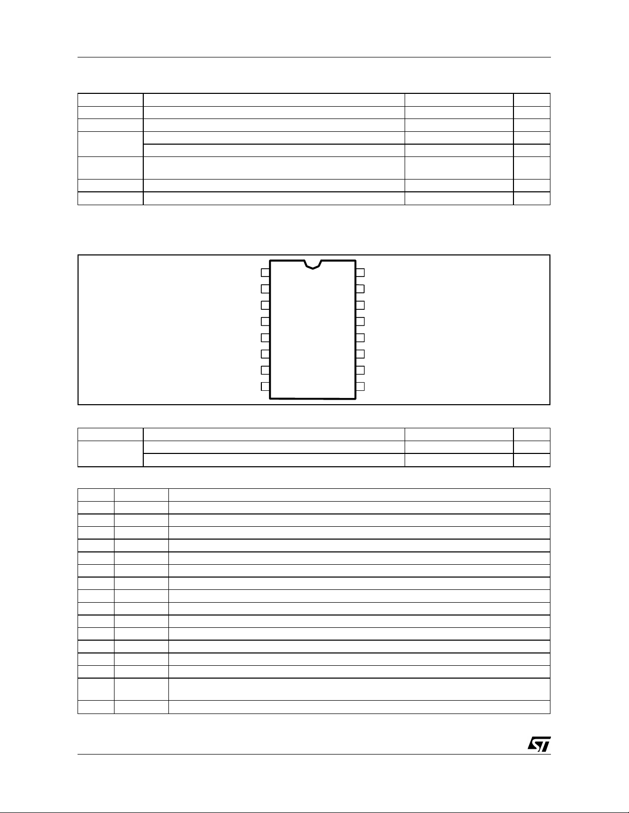
PACKAGE: DIP16 AND SO16
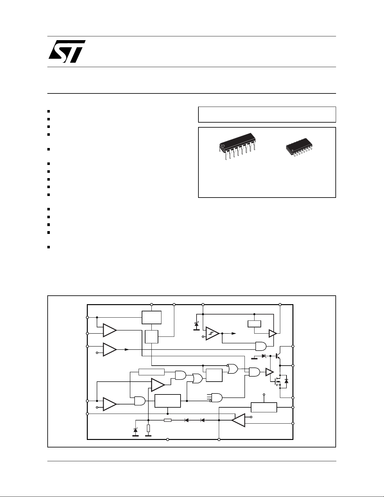
DESCRIPTION
This primary controller I.C., developed in BCD60II
technology, has been designed to implement off
L5991A
MULTIPOWER BCD TECHNOLOGY
DIP16 SO16
ORDERING NUMBERS:
L5991D/L5991AD (SO16)
line or DC-DC power supply applications using a
fixed frequency current mode control.
Based on a standard current mode PWM controller this device includes some features such as
programmable soft start, IN/OUT synchronization,
disable (to be used for over voltage protection and
for power management), precise maximum Duty
Cycle Control, 100ns leading edge blanking on
current sense, pulse by pulse current limit, overcurrent protection with soft start intervention, and
Standby function for oscillator frequency reduction
when the converter is lightly loaded.
L5991/L5991A (DIP16)
BLOCK DIAGRAM
2
RCT
3
DC
14
DIS
2.5V
13
ISEN
1.2V
SS
7
August 2001
+
-
-
+
OVER CURRENT
+
-
DIS
BLANKING
1V R
SYNC DC-LIM
TIMING
T
PWM
FAULT
SOFT-START
2R
12
SGND COMP
25V
15V/10V
VREF OK
CLK
DIS
V
CC
Vref
+
PWM UVLO
-
SQ
R
STAND-BY
+
2.5V
E/A
-
6
13V
VREF
VREF
48151
D97IN725A
9
V
C
10
OUT
11
PGND
16
ST-BY
5
VFB
1/23
L5991 - L5991A
ABSOLUTE MAXIMUM RATINGS
Symbol Parameter Value Unit
V
CC
I
OUT
P
tot
T
j
T
stg
(*) maximum package power dissipation limits must be observed
PIN CONNECTION
Supply Voltage (ICC < 50mA) (*) selflimit V
Output Peak Pulse Current 1.5 A
Analog Inputs & Outputs (6,7) -0.3 to 8 V
Analog Inputs & Outputs (1,2,3,4,5,15,14, 13, 16) -0.3 to 6 V
Power Dissipation @ T
@ T
= 70°C (DIP16)
amb
= 50°C (SO16)
amb
1
0.83
Junction Temperature, Operating Range -40 to 150 °C
Storage Temperature, Operating Range -55 to 150 °C
W
W
SYNC
RCT
DC
VREF
VFB
COMP
SS
V
CC
1
2
3
4
5
6
7OUT
8V
15
14
13
12
11
10
ST-BY16
DC-LIM
DIS
ISEN
SGND
PGND
9
C
THERMAL DATA
Symbol Parameter Value Unit
R
th j-amb
Thermal Resistance Junction -Ambient
Thermal Resistance Junction -Ambient
(DIP16)
(SO16)
80 °C/W
120 °C/W
PIN FU NCTIONS
N. Name Function
1 SYNC Synchronization. A synchronization pulse terminates the PWM cycle and discharges Ct
2 RCT Oscillator pin for external C
3 DC Duty Cycle control
4 VREF 5.0V +/-1.5% reference voltage @ 25°C
5 VFB Error Amplifier Inverting input
6 COMP Error Amplifier Output
7 SS Soft start pin for external capacitor Css
8V
9V
CC
C
Supply for internal "Signal" circuitry
Supply for Power section
10 OUT High current totem pole output
11 PGND Power ground
12 SGND Signal ground
13 ISEN Current sense
14 DIS Disable. It must never be left floating. TIE to SGND if not used.
15 DC-LIM Connecting this pin to Vref, DC is limited to 50%. If it is left floating or grounded no limitation is
imposed
16 ST-BY Standby. Connect a resistor to RCT. Connect to VREF or floating if not used.
, RA, RB components
T
2/23
L5991 - L5991A
ELECTRICAL CHARACTERI STICS
CC
= 15V; Tj = 0 to 105°C; RT = 13.3kΩ (*) CT = 1nF;
(V
unless otherwise specified.)
Symbol Parameter Test Condition Min. Typ. Max. Unit
REFERENCE SECTION
V
REF
T
S
I
OS
OSCILLATOR SECTION
ERROR AMPLIFIER SECTION
V
I
G
OPL
SVR Supply Voltage Rejection V
V
OL
V
OH
I
O
S
R
PWM CURRENT SENSE SECTION
I
b
I
S
V
t
SOFT START SECTION
I
SSC
I
SSD
V
SSSAT
V
SSCLAMP
LEADING EDGE BLANKING
OUTPUT SECTION
V
OL
V
OH
V
OUT CLAMP
(*) RT = RA//RB, RA = RB = 27kΩ, see Fig. 23.
Output Voltage Tj = 25°C; IO = 1mA 4.925 5.0 5.075 V
Line Regulation V
Load Regulation I
= 12 to 20V; Tj = 25°C 2.0 10 mV
CC
= 1 to 10mA; Tj = 25°C 2.0 10 mV
O
Temperature Stability 0.4 mV/°C
Total Variation Line, Load, Temperature 4.80 5.0 5.130 V
Short Circuit Current Vref = 0V 30 150 mA
Power Down/UVLO V
= 6V; I
CC
Initial Accuracy pin 15 = Vref; T
pin 15 = Vref; V
V
pin 15 = Vref; V
V
Duty Cycle pin 3 = 0,7V, pin 15 = V
pin 3 = 0.7V, pin 15 = OPEN
pin 3 = 3.2V, pin 15 = V
pin 3 = 3.2V, pin 15 = OPEN
= 0.5mA 0.2 0.5 V
sink
= 25°C; V
j
= 12 to 20V
CC
comp
= 12 to 20V
CC
comp
= 4.5V 95 100 105 kHz
comp
93 100 107 kHz
= 4.5V
46.5 50 53.5 kHz
= 2V
REF
0
0
REF
47
93
Duty Cycle Accuracy pin 3 = 2.79V, pin 15 = OPEN 75 80 85 %
Oscillator Ramp Peak 2.8 3.0 3.2 V
Oscillator Ramp Valley 0.75 0.9 1.05 V
Input Bias Current V
Input Voltage V
Open Loop Gain V
Output Low Voltage I
Output High Voltage I
Output Source Current V
Output Sink Current V
to GND 0.2 3.0 µA
FB
= V
COMP
COMP
CC
sink
source
COMP
COMP
FB
= 2 to 4V 60 90 dB
= 12 to 20V 85 dB
= 2mA 1.1 V
= 0.5mA, VFB = 2.3V 5 6 V
> 4V, VFB = 2.3V 0.5 1.3 2.5 mA
= 1.1V, VFB = 2.7V 2 6 mA
2.42 2.5 2.58 V
Unit Gain Bandwidth 1.7 4 MHz
Slew Rate 8 V/µs
Input Bias Current I
Maximum Input Signal V
= 0 3 15 µA
sen
= 5V 0.92 1.0 1.08 V
COMP
Delay to Output 70 100 ns
Gain 2.85 3 3.15 V/V
Fault Threshold Voltage 1.1 1.2 1.3 V
SS Charge Current Tj = 25°C 142026µA
SS Discharge Current VSS = 0.6V Tj = 25°C 5 10 15 µA
SS Saturation Voltage DC = 0% 0.6 V
SS Clamp Voltage 7 V
Internal Masking Time 100 ns
Output Low Voltage IO = 250mA 1.0 V
Output High Voltage IO = 20mA; VCC = 12V 10 10.5 V
I
= 200mA; VCC = 12V 9 10 V
O
Output Clamp Voltage IO = 5mA; VCC = 20V 13 V
Collector Leakage V
= 20V VC = 24V 2 20 µA
CC
%
%
%
%
3/23
L5991 - L5991A
ELECTRICAL CHARACTERI STICS
(continued.)
Symbol Parameter Test Condition Min. Typ. Max. Unit
OUTPUT SECTION
Fall Time C
O
C
O
= 1nF
= 2.5nF
Rise Time CO = 1nF
C
= 2.5nF
O
UVLO Saturation VCC = VC = 0 to V
CCON; Isink
= 10mA 1.0 V
20
35
50
70
60 ns
100 ns
SUPPLY SECTION
V
CCON
V
CCOFF
V
Startup voltage
Minimum Operating
Voltage
hys
I
S
I
op
I
q
V
Z
UVLO Hysteresis
Start Up Current Before Turn-on at:
V
= VC = V
CC
CCON
-0.5V
Operating Current CT = 1nF, RT = 13.3kΩ, CO =1nF 9 13 mA
Quiescent Current (After turn on), CT = 1nF,
R
= 13.3kΩ, CO =0nF
T
Zener Voltage I8 = 20mA 21 25 30 V
L5991
L5991A
L5991
L5991A
L5991
L5991A
14
7.8
9
7
4.5
0.5
15
8.4
10
7.6
5
0.8
16
9
11
8.2
40 75 120 µA
7.0 10 mA
STANDBY FUNCTION
I
V
REF-VST-BY
V
T1
Standby Threshold V
= 2mA 45 mV
ST-BY
Falling 2.5 V
comp
V
Rising 4.0 V
comp
SYNCHRONIZATION SECTION
Master Operation
V
1
I
1
Clock Amplitude I
Clock Source Current Vclock = 3.5V 3 7 mA
= 0.8mA 4 V
SOURCE
Slave Operation
V
1
Sync Pulse Low Level 1 V
High Level 3.5 V
I
1
Sync Pulse Current VSYNC = 3.5V 0.5 mA
OVER CURRENT PROTECTION
V
t
Fault Threshold Voltage 1.1 1.2 1.3 V
DISABLE SECTION
Shutdown threshold 2.4 2.5 2.6 V
= 0 to 3V -1 1 µA
pin14
VCC = 15V 330 µA
I
qSH
Input Bias Current V
Quiescent current After
Disable
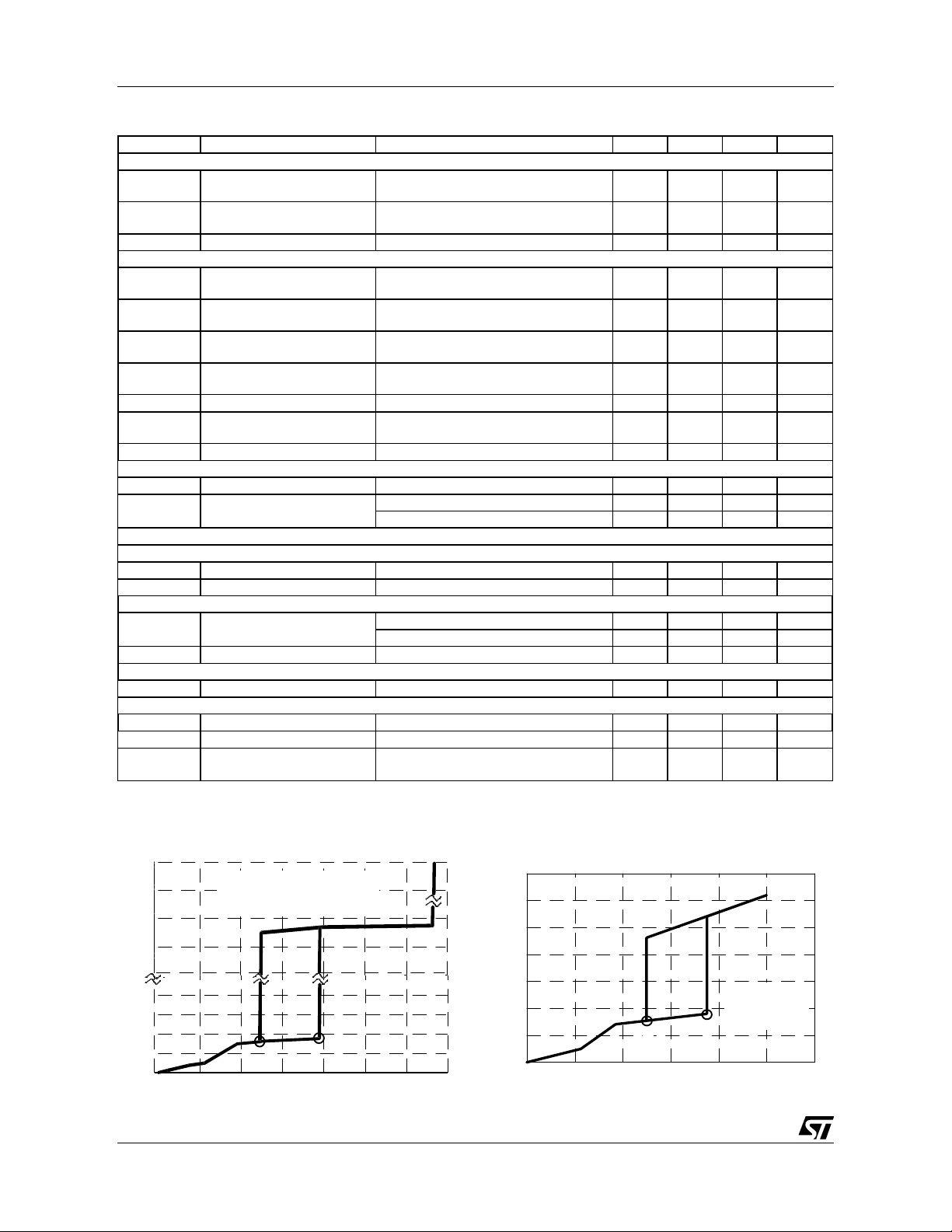
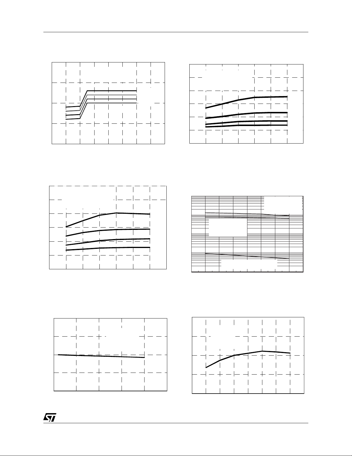
Figure 1. L5991 - Quiescent current vs. input
voltage.
(X = 7.6V and Y= 8.4V for L5991A)
Iq [m A ]
30
20
8
6
4
0.2
0.15
0.1
0.05
0
04 8
V14 = 0, Pin2 = open
Tj = 25°C
X
12 16 20 24
Y
Vcc [V]
28
Figure 2. L5991 - Quiescent current vs. input
voltage (after disable).
(X = 7.6V and Y= 8.4V for L5991A)
Iq [µ A ]
350
300
250
200
150
100
50
0
0 4 8 12 16 20 24
X
Vcc [V]
V14 = Vref
Tj = 25 °C
Y
ns
ns
V
V
V
V
V
V
4/23
)
L5991 - L5991A
Figure 3. Quiescent current vs. input voltage.
Iq [m A ]
9.0
V14 = 0, V5 = Vref
8.5
8.0
7.5
7.0
8 1012141618202224
Rt = 4.5Kohm,Tj = 25°C
1Mhz
500K hz
300K hz
100K hz
Vc c [V]
Figure 5. Quiescent current vs. input voltage
and switching fre que nc y .
Iq [mA ]
36
Co = 1nF, Tj = 25°C
30
24
18
12
6
0
8 10121416182022
DC = 100 %
1MHz
500KHz
300KHz
100KHz
Vcc [V]
Figure 4. Quiescent current vs. input voltage
and switching frequency.
Iq [m A]
36
30
24
18
12
6
0
Co = 1nF, Tj = 25°C
DC = 0%
1MHz
500KHz
300KHz
100KHz
8 10121416182022
Vcc [V]
Figure 6. IC Consumption vs. Temperature.
[mA]
100
10
Quiescent current
Vcc =15V, after turn-on
RT=13.3 kΩ, CT=1nF
1
DC = 0
0.1
Start-up current
Vc=Vcc= Vccon-0.5V , before turn-on
0.01
-50 -25 0 25 50 75 100 125 150
Junction temperature [˚C]
Operating current
Vcc =15V, after turn-on
RT=13.3kΩ, CT=1nF
DC=75%, Co=1nF
Figure 7. Reference voltage vs. load current.
Vref [V]
5.1
5.05
5
4.95
4.9
0 5 10 15 20 25
Vcc=15V
Tj = 25°C
Iref [mA]
Figure 8. Vref vs. junction temperature.
Vref [V])
5.1
5.05
5
4.95
4.9
-50 -25 0 25 50 75 100 125 150
Vcc = 15V
Iref = 1mA
Tj (°C
5/23
L5991 - L5991A
Figure 9. Vref vs. junction temperature.
Vref [V]
5.1
Vcc = 15V
5.05
5
4.95
4.9
-50 -25 0 25 50 75 100 125 150
Iref= 20mA
Tj (°C)
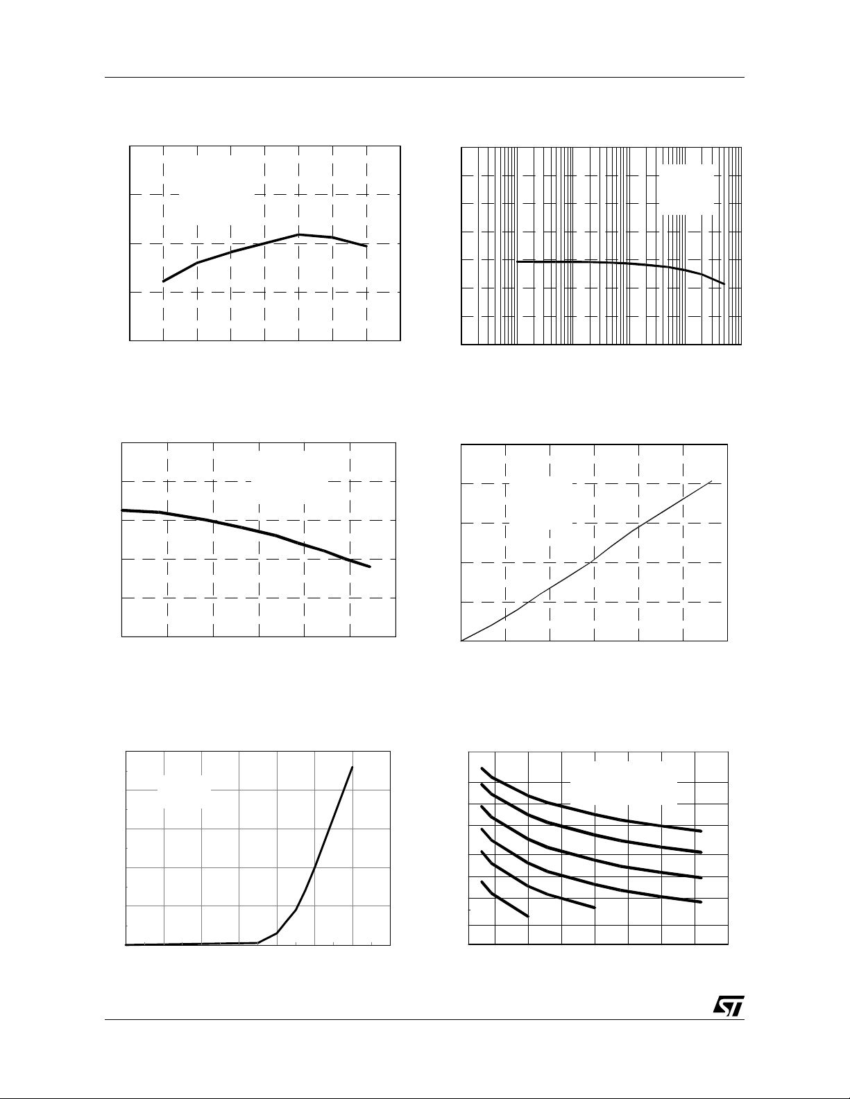
Figure 11. Output saturation.
Vsa t = V [V]
16
14
12
10
Vcc = Vc = 15V
Tj = 25°C
Figure 10. Vref SVRR vs. switching frequency.
SVRR (dB)
120
80
40
0
1 10 100 1000 10000
fsw (Hz)
Vcc=15V
Vp-p=1V
Figure 12. Output saturation.
Vs at = V [V]
2.5
2
1.5
10
Vcc = Vc = 15V
Tj = 25°C
10
8
6
0 0.2 0.4 0.6 0.8 1 1.2
Isource [A]
Figure 13. UVLO Saturation
Ipin10 [mA]
50
40
30
20
10
0
Vcc < Vccon
before turn-on
0 200 400 600 800 1,000 1,200 1,400
Vp in 1 0 [mV]
1
0.5
0
0 0.2 0.4 0.6 0.8 1 1.2
Isink [A]
Figure 14. Timing resistor vs. switching frequency.
fsw (KHz)
5000
2000
1000
500
200
100
50
20
10
5.6nF
10 20 30 40
Vcc = 15V, V15 =0V
Tj = 25°C
2.2nF
Rt (kohm)
100pF
220pF
470pF
1nF
6/23
)
L5991 - L5991A
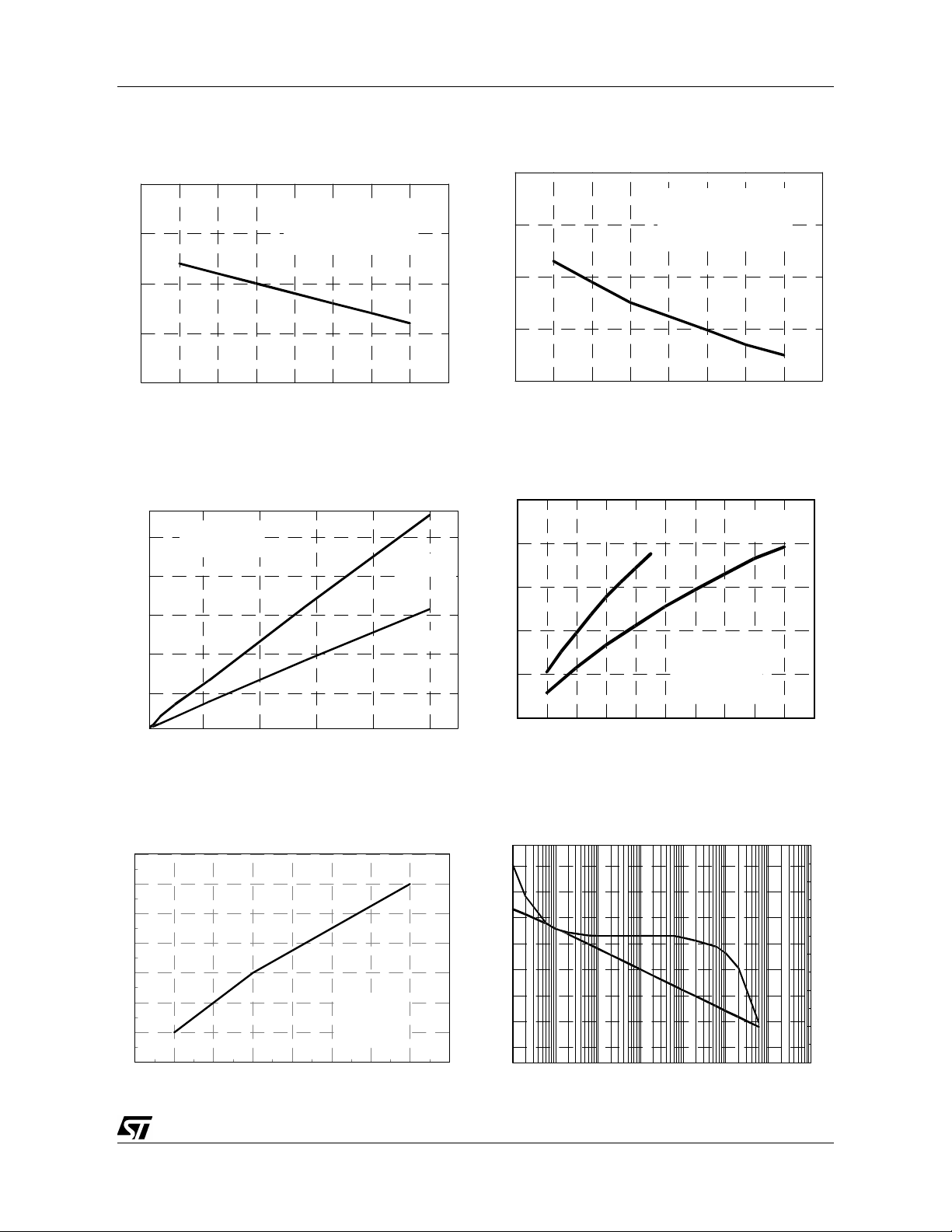
Figure 15. Switching frequency vs. tempera-
ture.
fsw (KHz)
320
Rt= 4.5Kohm, Ct = 1nF
310
300
290
280
-50 -25 0 25 50 75 100 125 150
Vcc = 15V, V15=Vref
Tj (°C)
Figure 17. Dead time vs Ct.
Dea d time [ns]
1,500
1,200
900
600
300
Rt =4.5Kohm
V15 = 0V
V15 = Vref
Figure 16. Switching freque nc y v s. t emp er atu re .
fsw (KHz)
320
Rt= 4.5Kohm, Ct = 1nF
310
Vcc = 15V, V15= 0
300
290
280
-50 -25 0 25 50 75 100 125 150
Tj (°C)
Figure 18. Maximum Duty Cycle vs Vpin3.
DC Control Voltage Vpin3 [V]
3.5
V15 = 0V
2.5
1.5
V15 = Vref
3
2
Rt = 4.5Kohm,
Ct = 1nF
246810
Timing capacitor Ct [nF]
Figure 19. Delay to out put vs jun ction temperat ure.
Delay to output (ns)
42
40
38
36
34
32
30
28
-50 -25 0 25 50 75 100 125 150
Tj (°C
PIN10 = OPEN
1V pulse
on PIN13
1
0 102030405060708090100
Duty Cycle [%]
Figure 20. E/A frequency response.
G [dB]
150
100
50
0
0.01 0.1 1 10 10 0 1000 10000 100000
f (KHz)
Phase
140
120
100
80
60
40
20
7/23
 Loading...