

4 A continuous (more than 5 A pulsed) step-down switching
regulator with synchronous rectification
Features
■ 4 A output current (more than 5 pulsed)
■ Operating input voltage from 2.9 V to 18 V
■ External 1.8 V ± 2% reference voltage
■ Output voltage from 0.6 to input voltage
■ MLCC compatible
■ 200 ns T
■
Programmable UVLO matches 3.3 V, 5 V and
12 V bus
■ F
SW
■ Voltage feed-forward
■ Zero load current operation
■ Programmable current limit on both switches
■ Programmable sink current capability
■ Pre-bias start up capability
■ Thermal shutdown
ON
programmable up to 1 MHz
L5989D
HTSSOP 16
Applications
■ Consumer: STB, DVD, LCD TV, VCR, car
radio, LCD monitors
■ Networking: XDSL, modems, routers and
switches
■ Computer and peripherals: printers, audio /
graphic cards, optical storage, hard disk drive
■ Industrial: DC-DC modules, factory automation
■ HC LED driving
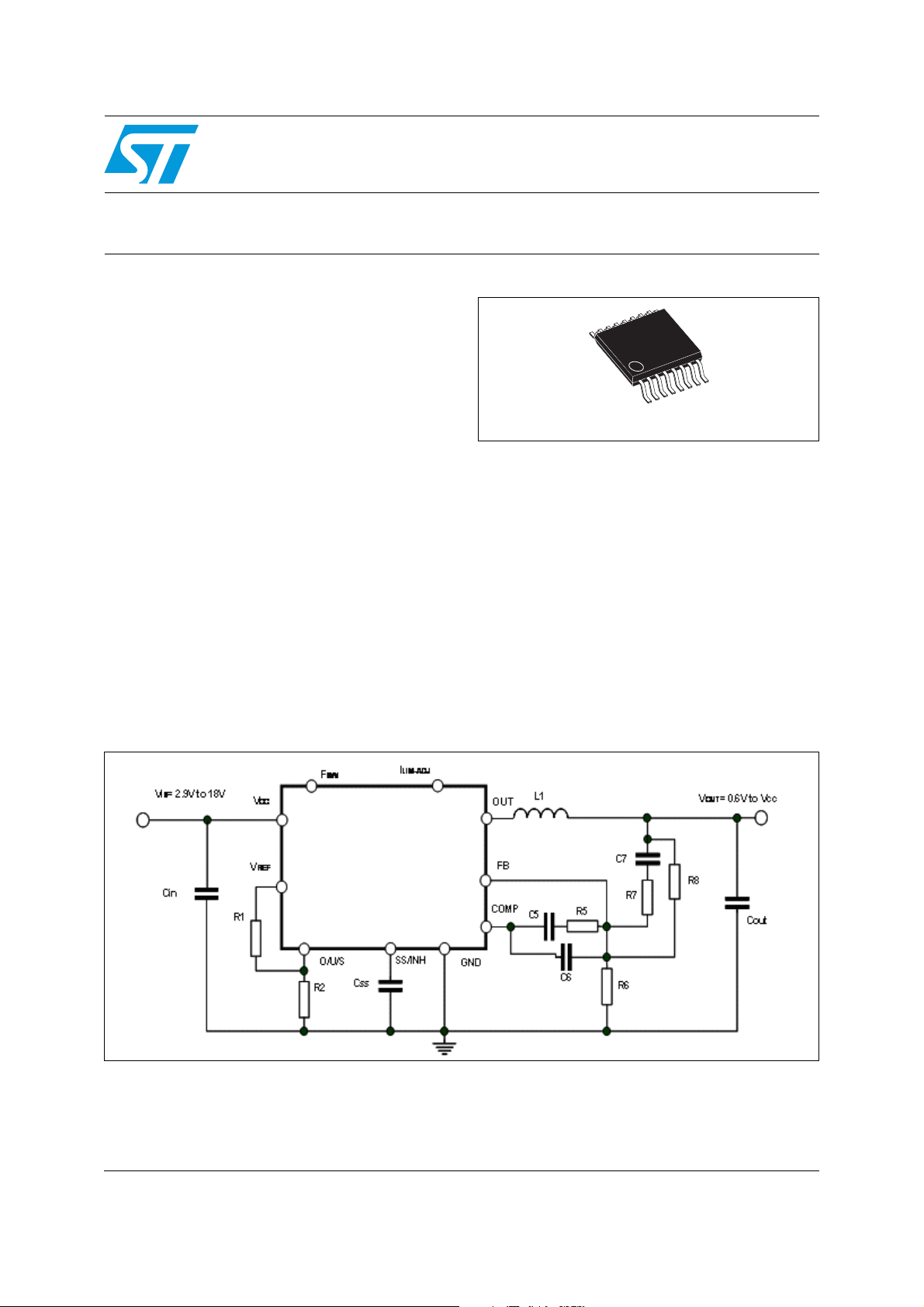
Figure 1. Test application circuit
L5989D
January 2010 Doc ID 15778 Rev 3 1/51
www.st.com
51

Contents L5989D
Contents
1 Description . . . . . . . . . . . . . . . . . . . . . . . . . . . . . . . . . . . . . . . . . . . . . . . . . 6
2 Pin function . . . . . . . . . . . . . . . . . . . . . . . . . . . . . . . . . . . . . . . . . . . . . . . . 7
3 Maximum ratings . . . . . . . . . . . . . . . . . . . . . . . . . . . . . . . . . . . . . . . . . . . . 8
4 Electrical characteristics . . . . . . . . . . . . . . . . . . . . . . . . . . . . . . . . . . . . . 9
5 Functional description . . . . . . . . . . . . . . . . . . . . . . . . . . . . . . . . . . . . . . 12
5.1 Multifunction pin . . . . . . . . . . . . . . . . . . . . . . . . . . . . . . . . . . . . . . . . . . . . 13
5.2 Oscillator . . . . . . . . . . . . . . . . . . . . . . . . . . . . . . . . . . . . . . . . . . . . . . . . . 15
5.3 External voltage reference . . . . . . . . . . . . . . . . . . . . . . . . . . . . . . . . . . . . 17
5.4 Soft-start . . . . . . . . . . . . . . . . . . . . . . . . . . . . . . . . . . . . . . . . . . . . . . . . . . 17
5.5 Monitoring and protections . . . . . . . . . . . . . . . . . . . . . . . . . . . . . . . . . . . . 18
5.5.1 Overvoltage . . . . . . . . . . . . . . . . . . . . . . . . . . . . . . . . . . . . . . . . . . . . . . 18
5.5.2 Current limiting . . . . . . . . . . . . . . . . . . . . . . . . . . . . . . . . . . . . . . . . . . . . 20
5.5.3 UVLO . . . . . . . . . . . . . . . . . . . . . . . . . . . . . . . . . . . . . . . . . . . . . . . . . . . 21
5.5.4 Thermal shutdown . . . . . . . . . . . . . . . . . . . . . . . . . . . . . . . . . . . . . . . . . 22
5.6 Power Good . . . . . . . . . . . . . . . . . . . . . . . . . . . . . . . . . . . . . . . . . . . . . . . 22
5.7 Minimum on time . . . . . . . . . . . . . . . . . . . . . . . . . . . . . . . . . . . . . . . . . . . 22
5.8 Error amplifier . . . . . . . . . . . . . . . . . . . . . . . . . . . . . . . . . . . . . . . . . . . . . . 23
6 Application information . . . . . . . . . . . . . . . . . . . . . . . . . . . . . . . . . . . . . 24
6.1 Input capacitor selection . . . . . . . . . . . . . . . . . . . . . . . . . . . . . . . . . . . . . . 24
6.2 Inductor selection . . . . . . . . . . . . . . . . . . . . . . . . . . . . . . . . . . . . . . . . . . . 25
6.3 Output capacitor selection . . . . . . . . . . . . . . . . . . . . . . . . . . . . . . . . . . . . 26
6.4 Compensation network . . . . . . . . . . . . . . . . . . . . . . . . . . . . . . . . . . . . . . 27
6.4.1 Type III compensation network . . . . . . . . . . . . . . . . . . . . . . . . . . . . . . . 28
6.4.2 Type II compensation network . . . . . . . . . . . . . . . . . . . . . . . . . . . . . . . . 32
6.5 R.M.S. current of the embedded power MOSFETs . . . . . . . . . . . . . . . . . 35
6.6 Thermal considerations . . . . . . . . . . . . . . . . . . . . . . . . . . . . . . . . . . . . . . 36
6.7 Layout considerations . . . . . . . . . . . . . . . . . . . . . . . . . . . . . . . . . . . . . . . . 39
6.8 Application circuit . . . . . . . . . . . . . . . . . . . . . . . . . . . . . . . . . . . . . . . . . . . 41
2/51 Doc ID 15778 Rev 3

L5989D Contents
7 Typical characteristics . . . . . . . . . . . . . . . . . . . . . . . . . . . . . . . . . . . . . . 44
8 Package mechanical data . . . . . . . . . . . . . . . . . . . . . . . . . . . . . . . . . . . . 47
9 Order codes . . . . . . . . . . . . . . . . . . . . . . . . . . . . . . . . . . . . . . . . . . . . . . . 49
10 Revision history . . . . . . . . . . . . . . . . . . . . . . . . . . . . . . . . . . . . . . . . . . . 50
Doc ID 15778 Rev 3 3/51

List of table L5989D
List of table
Table 1. Pinout description . . . . . . . . . . . . . . . . . . . . . . . . . . . . . . . . . . . . . . . . . . . . . . . . . . . . . . . . . 7
Table 2. Absolute maximum ratings . . . . . . . . . . . . . . . . . . . . . . . . . . . . . . . . . . . . . . . . . . . . . . . . . . 8
Table 3. Thermal data. . . . . . . . . . . . . . . . . . . . . . . . . . . . . . . . . . . . . . . . . . . . . . . . . . . . . . . . . . . . . 8
Table 4. Electrical characteristic . . . . . . . . . . . . . . . . . . . . . . . . . . . . . . . . . . . . . . . . . . . . . . . . . . . . . 9
Table 5. A/D voltage windows . . . . . . . . . . . . . . . . . . . . . . . . . . . . . . . . . . . . . . . . . . . . . . . . . . . . . 14
Table 6. UOS voltage biasing . . . . . . . . . . . . . . . . . . . . . . . . . . . . . . . . . . . . . . . . . . . . . . . . . . . . . . 14
Table 7. FSW resistor examples. . . . . . . . . . . . . . . . . . . . . . . . . . . . . . . . . . . . . . . . . . . . . . . . . . . . 16
Table 8. ILIM-ADJ resistor examples . . . . . . . . . . . . . . . . . . . . . . . . . . . . . . . . . . . . . . . . . . . . . . . . 21
Table 10. Input capacitors . . . . . . . . . . . . . . . . . . . . . . . . . . . . . . . . . . . . . . . . . . . . . . . . . . . . . . . . . 25
Table 11. Inductors . . . . . . . . . . . . . . . . . . . . . . . . . . . . . . . . . . . . . . . . . . . . . . . . . . . . . . . . . . . . . . . 26
Table 12. Output capacitors . . . . . . . . . . . . . . . . . . . . . . . . . . . . . . . . . . . . . . . . . . . . . . . . . . . . . . . . 27
Table 13. Component list . . . . . . . . . . . . . . . . . . . . . . . . . . . . . . . . . . . . . . . . . . . . . . . . . . . . . . . . . . 42
Table 14. Component list . . . . . . . . . . . . . . . . . . . . . . . . . . . . . . . . . . . . . . . . . . . . . . . . . . . . . . . . . . 43
Table 15. HTSSOP16 mechanical data . . . . . . . . . . . . . . . . . . . . . . . . . . . . . . . . . . . . . . . . . . . . . . . 47
Table 16. Order codes . . . . . . . . . . . . . . . . . . . . . . . . . . . . . . . . . . . . . . . . . . . . . . . . . . . . . . . . . . . . 49
Table 17. Document revision history . . . . . . . . . . . . . . . . . . . . . . . . . . . . . . . . . . . . . . . . . . . . . . . . . 50
4/51 Doc ID 15778 Rev 3

L5989D List of figures
List of figures
Figure 1. Test application circuit . . . . . . . . . . . . . . . . . . . . . . . . . . . . . . . . . . . . . . . . . . . . . . . . . . . . . 1
Figure 2. Pin connection . . . . . . . . . . . . . . . . . . . . . . . . . . . . . . . . . . . . . . . . . . . . . . . . . . . . . . . . . . . 7
Figure 3. Voltage mode control loop . . . . . . . . . . . . . . . . . . . . . . . . . . . . . . . . . . . . . . . . . . . . . . . . . 12
Figure 4. Internal block diagram . . . . . . . . . . . . . . . . . . . . . . . . . . . . . . . . . . . . . . . . . . . . . . . . . . . . 12
Figure 5. Oscillator circuit block diagram . . . . . . . . . . . . . . . . . . . . . . . . . . . . . . . . . . . . . . . . . . . . . . 15
Figure 6. Sawtooth: voltage feed forward . . . . . . . . . . . . . . . . . . . . . . . . . . . . . . . . . . . . . . . . . . . . . 16
Figure 7. Sawtooth: frequency adjust . . . . . . . . . . . . . . . . . . . . . . . . . . . . . . . . . . . . . . . . . . . . . . . . 16
Figure 8. OVP not latched . . . . . . . . . . . . . . . . . . . . . . . . . . . . . . . . . . . . . . . . . . . . . . . . . . . . . . . . . 18
Figure 9. OVP latched . . . . . . . . . . . . . . . . . . . . . . . . . . . . . . . . . . . . . . . . . . . . . . . . . . . . . . . . . . . . 19
Figure 10. Constant current protection at extreme duty cycles . . . . . . . . . . . . . . . . . . . . . . . . . . . . . . 21
Figure 11. Minimum TON. . . . . . . . . . . . . . . . . . . . . . . . . . . . . . . . . . . . . . . . . . . . . . . . . . . . . . . . . . . 23
Figure 12. Type III compensation network. . . . . . . . . . . . . . . . . . . . . . . . . . . . . . . . . . . . . . . . . . . . . . 29
Figure 13. Open loop gain: module bode diagram. . . . . . . . . . . . . . . . . . . . . . . . . . . . . . . . . . . . . . . . 29
Figure 14. Open loop gain bode diagram with ceramic output capacitor . . . . . . . . . . . . . . . . . . . . . . . 31
Figure 15. Type II compensation network . . . . . . . . . . . . . . . . . . . . . . . . . . . . . . . . . . . . . . . . . . . . . . 32
Figure 16. Open loop gain: module bode diagram. . . . . . . . . . . . . . . . . . . . . . . . . . . . . . . . . . . . . . . . 32
Figure 17. Open loop gain bode diagram with high ESR output capacitor . . . . . . . . . . . . . . . . . . . . . 34
Figure 18. Maximum continuos output current vs. duty cycle . . . . . . . . . . . . . . . . . . . . . . . . . . . . . . . 35
Figure 19. Switching losses . . . . . . . . . . . . . . . . . . . . . . . . . . . . . . . . . . . . . . . . . . . . . . . . . . . . . . . . . 36
Figure 20. Estimation of the internal power losses . . . . . . . . . . . . . . . . . . . . . . . . . . . . . . . . . . . . . . . 37
Figure 21. Estimation of the internal power losses . . . . . . . . . . . . . . . . . . . . . . . . . . . . . . . . . . . . . . . 38
Figure 22. Measurement of the thermal impedance of the evaluation board. . . . . . . . . . . . . . . . . . . . 39
Figure 23. Top board layout . . . . . . . . . . . . . . . . . . . . . . . . . . . . . . . . . . . . . . . . . . . . . . . . . . . . . . . . . 40
Figure 24. Bottom board layout . . . . . . . . . . . . . . . . . . . . . . . . . . . . . . . . . . . . . . . . . . . . . . . . . . . . . . 41
Figure 25. Demonstration board application circuit (fSW = 400 kHz) . . . . . . . . . . . . . . . . . . . . . . . . . 41
Figure 26. Demonstration board application circuit (fSW = 600 kHz) . . . . . . . . . . . . . . . . . . . . . . . . . 43
Figure 27. Junction temperature vs. fSW. . . . . . . . . . . . . . . . . . . . . . . . . . . . . . . . . . . . . . . . . . . . . . . 44
Figure 28. Junction temperature vs. fSW. . . . . . . . . . . . . . . . . . . . . . . . . . . . . . . . . . . . . . . . . . . . . . . 44
Figure 29. Junction temperature vs. fSW. . . . . . . . . . . . . . . . . . . . . . . . . . . . . . . . . . . . . . . . . . . . . . . 44
Figure 30. Junction temperature vs. VOUT . . . . . . . . . . . . . . . . . . . . . . . . . . . . . . . . . . . . . . . . . . . . . 44
Figure 31. Junction temperature vs. VOUT . . . . . . . . . . . . . . . . . . . . . . . . . . . . . . . . . . . . . . . . . . . . . 45
Figure 32. Junction temperature vs. VOUT . . . . . . . . . . . . . . . . . . . . . . . . . . . . . . . . . . . . . . . . . . . . . 45
Figure 33. Efficiency vs. output current . . . . . . . . . . . . . . . . . . . . . . . . . . . . . . . . . . . . . . . . . . . . . . . . 45
Figure 34. Efficiency vs. output current . . . . . . . . . . . . . . . . . . . . . . . . . . . . . . . . . . . . . . . . . . . . . . . . 45
Figure 35. Efficiency vs. output current . . . . . . . . . . . . . . . . . . . . . . . . . . . . . . . . . . . . . . . . . . . . . . . . 45
Figure 36. Load regulation . . . . . . . . . . . . . . . . . . . . . . . . . . . . . . . . . . . . . . . . . . . . . . . . . . . . . . . . . . 45
Figure 37. Line regulation . . . . . . . . . . . . . . . . . . . . . . . . . . . . . . . . . . . . . . . . . . . . . . . . . . . . . . . . . . 46
Figure 38. Load transient from 0 to 3 A . . . . . . . . . . . . . . . . . . . . . . . . . . . . . . . . . . . . . . . . . . . . . . . . 46
Figure 39. Soft-start . . . . . . . . . . . . . . . . . . . . . . . . . . . . . . . . . . . . . . . . . . . . . . . . . . . . . . . . . . . . . . . 46
Figure 40. Mechanical drawing . . . . . . . . . . . . . . . . . . . . . . . . . . . . . . . . . . . . . . . . . . . . . . . . . . . . . . 48
Doc ID 15778 Rev 3 5/51

Description L5989D
1 Description
The L5989D is a monolithic step down power switching regulator able to deliver a continuos
output current of 4 A to the load in most of the application conditions limited only by the
thermal performance (see Chapter 6.5 for details). The device is able to deliver more than
5 A to the load for a maximum time which is dependent on the thermal impedance of the
system and the specific operating conditions (see Chapter 6.6).
The input voltage can range from 2.9 V to 18 V. The device is capable of 100% duty cycle
operation thanks to the embedded high side PMOS switch which doesn’t need external
bootstrap capacitor to be driven.
The internal switching frequency is adjustable by external resistor and can be set
continuously from 100 kHz to 1 MHz.
The multifunction UOS pin allows to set-up properly the additional embedded features
depending on the value of the voltage level.
● U (UVLO): two UVLO thresholds can be selected to match the 3.3 V and 5 V or 12 V
input buses
● O (OVP): latched or not latched OVP protection selectable. In latched mode the
switching activity is interrupted until an UVLO or INH event happens
● S (SINK): the sink capability is always disabled during soft-start time to support pre-
biased output voltage. Afterwards the sink capability can be enabled or not depending
on the voltage set on the multifunction pin.
During soft-start phase a constant current protection is active to deliver extra current
necessary to load the output capacitor. The current limit protection is achieved by sensing
the current flowing in both embedded switches to assure an effective protection even at
extreme duty cycle operations. Finished the soft-start phase the current protection feature
triggers the “HICCUP” mode forcing the soft-start capacitor to be discharged and recharged.
The current thresholds of both switches can be adjusted in tracking by using an external
resistor to dimension the current protection accordingly to the local application.
The soft-start time is based on a constant current charge of an external capacitor. As a
consequence the time can be set accordingly to the value of the output capacitor.
The latest smart power technology BCD6 (Bipolar-CMOS-DMOS version 6) features a low
resistance of the embedded switches (35 mΩ typical for a NMOS, 50 mΩ typical for a
PMOS), achieving high efficiency levels.
The HTSSOP16 package with exposed pad accomplishes low R
(40°C/W), useful in
thJA
dissipating power internally generated during high output current / high frequency
operations.
6/51 Doc ID 15778 Rev 3
L5989D Pin function
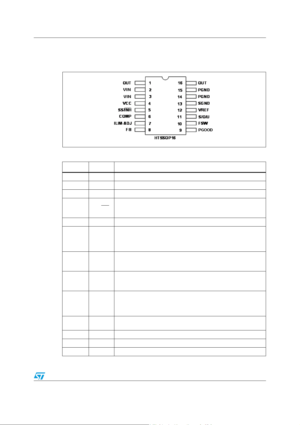
2 Pin function
Figure 2. Pin connection
Table 1. Pinout description
N. Name Description
1, 16 OUT Regulator output
2, 3 VIN Unregulated DC input voltage
4 VCC Unregulated DC signal input voltage
An external logic signal (active LOW) disables the device. In case the pin is
5 SS/INH
floating the device deliver a constant current (22 μA typ.) to charge the
soft-start capacitor (see Chapter 5.4)
6 COMP Error amplifier output for frequency compensation
Connecting a pull-up resistor to VREF or a pull-down resistor to GND the
7 ILIM-ADJ
internal current limit thresholds can be tuned to match the local application.
In case the pin is left floating no changes are applied to the default current
limit thresholds
Feedback input. Connecting the output voltage directly to this pin results in
8FB
a regulation voltage of 600 mV. An external resistive divider is required for
higher output voltages
Open collector output; low impedance if the feedback voltage is lower than
9 PGOOD
0.85 times the internal reference of the error amplifier. An hysteresis is
provided
Connecting a pull-up resistor to VREF or a pull-down resistor to GND the
10 FSW
internal oscillator frequency will be increased or decreased respectively. In
case the pin is left floating the predefined oscillator frequency
(400 kHz ± 10%) is active
11 U/O/S
12 VREF 1.8 V voltage reference
Multifunction pin used to program additional features: UVLO thresholds,
OVP latched/not latched, SINK enabled/disabled
13 SGND Signal ground
14, 15 PGND Power ground
Doc ID 15778 Rev 3 7/51
Maximum ratings L5989D
3 Maximum ratings
Table 2. Absolute maximum ratings
Symbol Parameter Value Unit
VCC Input voltage 20 V
VOUT Output DC voltage -0.3
(1)
to VCC
V
U/O/S, SS/INH
COMP, PGOOD,
,
Analog pins -0.3 to 4 V
Fsw, ILIM-ADJ
FB Feedback voltage 1.5 V
P
tot
T
J
T
STG
1. During the switching activity the negative peak voltage could reach -1.5 V without any damage for the
device
Power dissipation at TA < 60 °C 2.25 W
Junction temperature range -40 to 150 °C
Storage temperature range -55 to 150 °C
Table 3. Thermal data
Symbol Parameter Value Unit
R
thJA
Thermal resistance junction to ambient max 40
1. HTSSOP16 package mounted on ST demonstration board
(1)
°C/W
8/51 Doc ID 15778 Rev 3
L5989D Electrical characteristics
4 Electrical characteristics
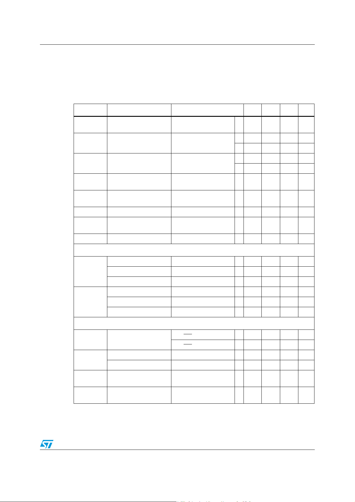
VCC = 12 V, TJ = 25 °C unless otherwise specified.
Table 4. Electrical characteristic
Symbol Parameter Test condition Min Typ Max Unit
Vcc
Rdson HS
Rdson LS
I
L HIGH SIDE
I
L LOW SIDE
f
SW
f
SW ADJ
Operating input voltage
range
High side MOSFET on
resistance
Low side MOSFET on
resistance
Maximum peak limiting
current
Maximum valley limiting
current
Vout = 0.6 V; Iout = 3 A 2.9 18 V
75 85 95 mΩ
Iout = 1.0 A
(1)
111 120 132 mΩ
62 67 72 mΩ
Iout = 1.0 A
I
I
= float 3.6 4 4.4 A
LIM-ADJ
= float 4.14 4.6 5.06 A
LIM-ADJ
(1)
92 100 106 mΩ
Switching frequency FSW = floating 360 400 440 kHz
Adjusted switching
frequency
R
FSW PULL DWN
= 27 kΩ 1000 kHz
D Duty cycle 0 100 %
Selectable undervoltage lock-out (UVLO)
Turn ON Vcc threshold 2.7 2.8 V
3.3 V BUS
Turn OFF Vcc threshold 2.4 2.5 V
Hysteresis 200 mV
Turn ON Vcc threshold 8 8.6 V
12 V BUS
Turn OFF Vcc threshold 6.8 7 V
Hysteresis 1 V
DC characteristic
I
SS
Soft-start current
V
V
= 2 V 22 μA
SS/INH
= 0 5 μA
SS/INH
Device ON level 0.8 V
INH
Device OFF level 0.3 V
I
q
I
q st-by
Quiescent current
Total stand-by quiescent
current
Duty Cycle = 0;
= 1 V
V
FB
3mA
35 μA
Doc ID 15778 Rev 3 9/51
Electrical characteristics L5989D
Table 4. Electrical characteristic (continued)
Symbol Parameter Test condition Min Typ Max Unit
Dynamic characteristic (see figure 1)
V
FB
Voltage feedback in
regulation
Error amplifier
V
OH
V
OL
I
O SOURCE
I
O SRCE LIM
I
O SINK
A
V0
High level output voltage VFB = 0.2 V; SS floating 3.1 V
Low level output voltage VFB = 1.0 V 0.1 V
Source output current VFB = 0.2 V
Source current limitation VFB = 0.2 V, V
Sink output current VFB = 1.0 V, V
DC open loop gain
PGOOD
Up threshold
(V
V
FB_PGOOD
FB_PGOOD
Low threshold
(V
FB_PGOOD
V
PGOOD
Reference section
V
REF
Reference voltage Vcc = 2.9 V to 18 V
/ VFB)
/ VFB)
2.9 V < VCC < 18 V
COMP
COMP
rising 81 85 90
V
FB
V
falling 77 82 86
FB
I
= -1 mA 0.4 V
PGOOD
(1)
0.592 0.6 0.609
(2)
25 mA
=3 V 2 mA
=0.5 V 30 mA
(2)
100 dB
1.756 1.8 1.837 V
(1)
1.754 1.8 1.852 V
0.595 0.6 0.605
V
%
V
FB
Line regulation
Load regulation I
Short circuit current 12 18 24 mA
Protections
V
FB_OVP
Overvoltage trip
FB_OVP
- VFB) / V
(V
FB
Bus thresholds
- UVLO 3.3 V bus
TH1
- OVP not latched
- No sink
- UVLO 3.3 V bus
TH2
- OVP not latched
- Sink
- UVLO 3.3 V bus
TH3
- OVP latched
- No sink
10/51 Doc ID 15778 Rev 3
Vcc = 2.9 V to 18 V
I
= 0 mA
REF
= 0 to 5 mA 7.5 15 mV
REF
V
rising 15 20 24 %
FB
(3)
00.2V
(3)
0.26 0.425 V
(3)
0.48 0.65 V
612mV
L5989D Electrical characteristics
Table 4. Electrical characteristic (continued)
Symbol Parameter Test condition Min Typ Max Unit
- UVLO 3.3 V bus
TH4
- OVP latched
(3)
0.71 0.875 V
- Sink
- UVLO 12 V bus
TH5
- OVP not latched
(3)
0.93 1.085 V
- No sink
- UVLO 12 V bus
TH6
- OVP not latched
(3)
1.16 1.31 V
- Sink
- UVLO 12 V bus
TH7
- OVP latched
(3)
1.385 1.525 V
- No sink
- UVLO 12 V bus
TH8
- OVP latched
(3)
1.615 VREF V
- Sink
1. Specification over the junction temperature range (TJ) of -40 to +125 °C are guaranteed by design,
characterization and statistical correlation
2. Guaranteed by design
= 4 V
3. V
CC
Doc ID 15778 Rev 3 11/51
Functional description L5989D
5 Functional description
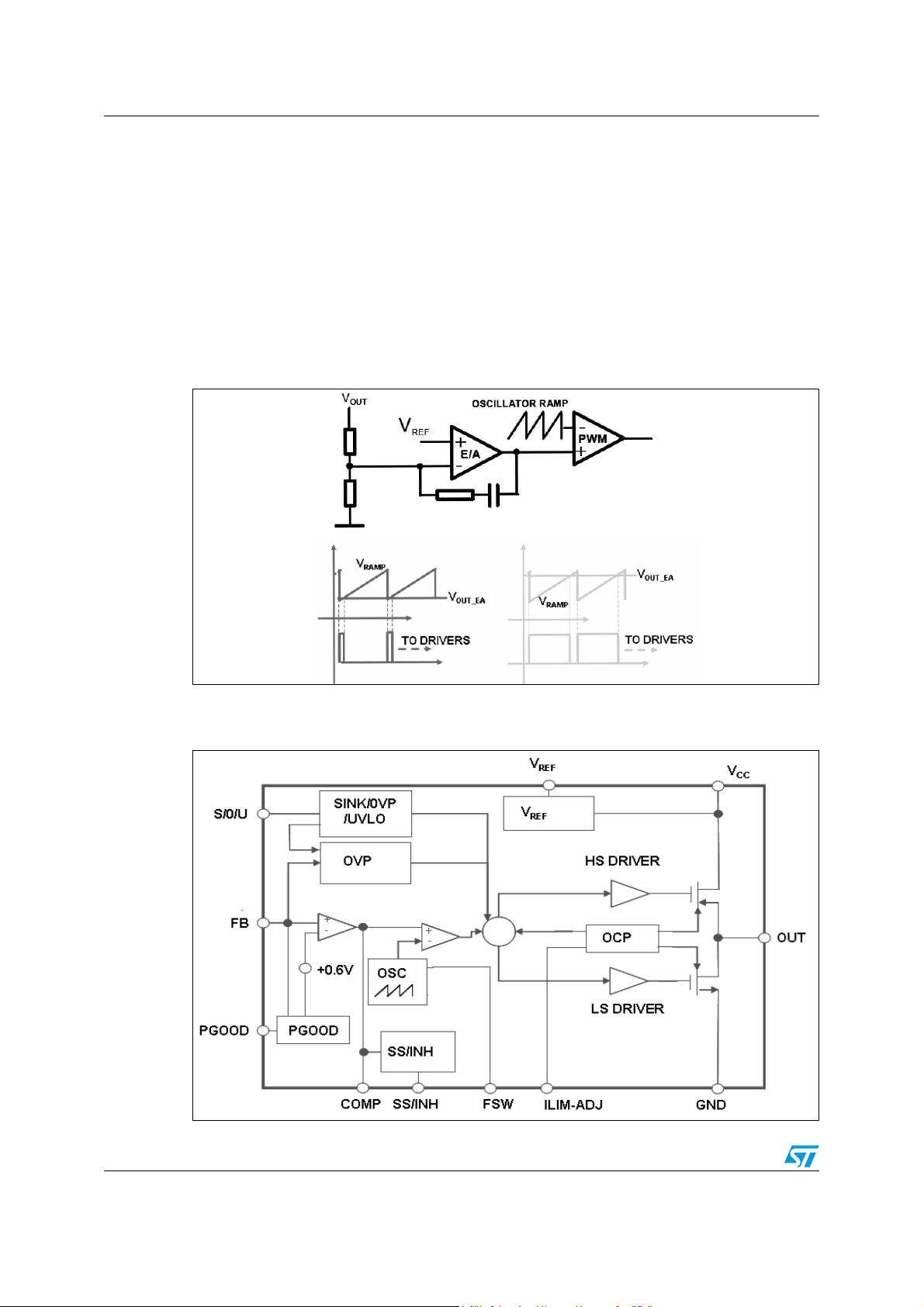
The L5989D is based on a voltage mode control loop. Therefore the duty ratio of the internal
switch is obtained through a comparison between a saw-tooth waveform (generated by an
oscillator) and the output voltage of the error amplifier as shown in Figure 3. The advantage
of this technique is the very short conduction time of the power elements thanks to the
proper operation of the control loop without a precise current sense, which instead is
required in current mode regulators. Thanks to this architecture the L5989D supports
extremely low conversion ratio (D = V
OUT/VIN
(up to 1 MHz).
Figure 3. Voltage mode control loop
) even at very high switching frequency
The main internal blocks are represented in Figure 4.
Figure 4. Internal block diagram
12/51 Doc ID 15778 Rev 3

L5989D Functional description
Below follows a brief description of the main blocks:
● A voltage pre-regulator supplies the internal circuitry. The external 1.8 V voltage
reference is supplied by this regulator.
● A voltage monitor circuit that checks the input and internal voltages
● A fully integrated sawtooth oscillator whose frequency is 400 kHz ± 10% when the Fsw
pin is floating. Its frequency can be increased/decreased connecting a proper resistor
to GND or VREF
● The internal current limitation circuitry monitors the current flowing in both embedded
switches to guarantee an effective protection even in extreme duty cycle conditions
● The over voltage protection (OVP) monitors the feedback voltage. If the voltage of this
pin overcomes the 20% of the internal reference value (600 mV ± 1%) it will force the
conduction of the low side switch until the overshoot is present
● A voltage mode amplifier. The inverting input and the output are externally available for
compensation
● A pulse width modulator (PWM) comparator and the relative logic to drive the
embedded switches
● The soft-start circuit charges an external capacitor with a constant current equal to
20 µA (typ.). The soft-start feature is realized clamping the output of the error amplifier
until the voltage across the capacitor is below 2.7 V
● The PGOOD is an open collector output: low impedance if the feedback voltage is
lower than 0.85 times the internal reference of the error amplifier. An hysteresis is
provided
● The circuitry related to the UOS multifunction pin is composed of a 3 bit A/D converter
and the decoding logic. It recognizes eight different voltage windows of a VREF voltage
magnitude for selecting additional features.
● An inhibit block for stand-by operation
● A circuit to realize the thermal protection function
5.1 Multifunction pin
The UOS pin is used to configure the device additional features accordingly to the voltage
bias imposed through VREF voltage partitioning.
The selectable options are:
● UVLO level: two pre-defined the under voltage lock out thresholds can be selected to
match the 3.3 V and 5 V or 12 V power bus
● SINK capability: this feature is always disabled during the soft-start period to be
compatible with pre-biased output voltages. After the soft-start phase, the synchronous
rectification can be enabled or not depending on the status of the UOS pin. Anyway, in
case an overvoltage is detected, the sink capability is always enabled to bring the FB
back to regulation as fast as possible
● OVP management: in case the latched mode is selected and an overvoltage event
recurs, the switching activity will be suspended until VCC is reapplied or the SS/INH
is toggled. Otherwise when the overvoltage transient is ended the regulator will work
accordingly to the load request without regulation discontinuity
The circuitry related to the UOS multifunction pin is composed of a 3 bit A/D converter and
the decoding logic. Table 5 shows the internal thresholds of each voltage window
pin
Doc ID 15778 Rev 3 13/51
Functional description L5989D
composing the VREF magnitude. The voltage biasing of the multifunction can be set
accordingly to table Table 6 .
Table 5. A/D voltage windows
UVLO OVP SINK
1.8 V
1.575 V
1.35 V
1.125 V
0.9 V
12 V BUS Latch Sink
12 V BUS Latch No sink
12 V BUS No latch Sink
12 V BUS No latch No sink
3.3 V BUS Latch Sink
0.675 V
3.3 V BUS Latch No sink
0.45 V
3.3 V BUS No latch Sink
0.225 V
3.3 V BUS No latch No sink
0 V
Table 6. UOS voltage biasing
R1 (kΩ)R2 (kΩ)V
0 N.C. 1.8 12 V bus Latch Sink
0.68 2.7 1.438 12 V bus Latch No sink
1.2 2.7 1.246 12 V bus No latch Sink
2 2.7 1.034 12 V bus No latch No sink
(V) UVLO OVP SINK
OUS
3.3 2.7 0.810 3.3 V bus Latch Sink
6.2 2.7 0.546 3.3 V bus Latch No sink
11 2.7 0.355 3.3 V bus No latch Sink
N.C. 0 0 3.3 V bus No latch No sink
14/51 Doc ID 15778 Rev 3
L5989D Functional description
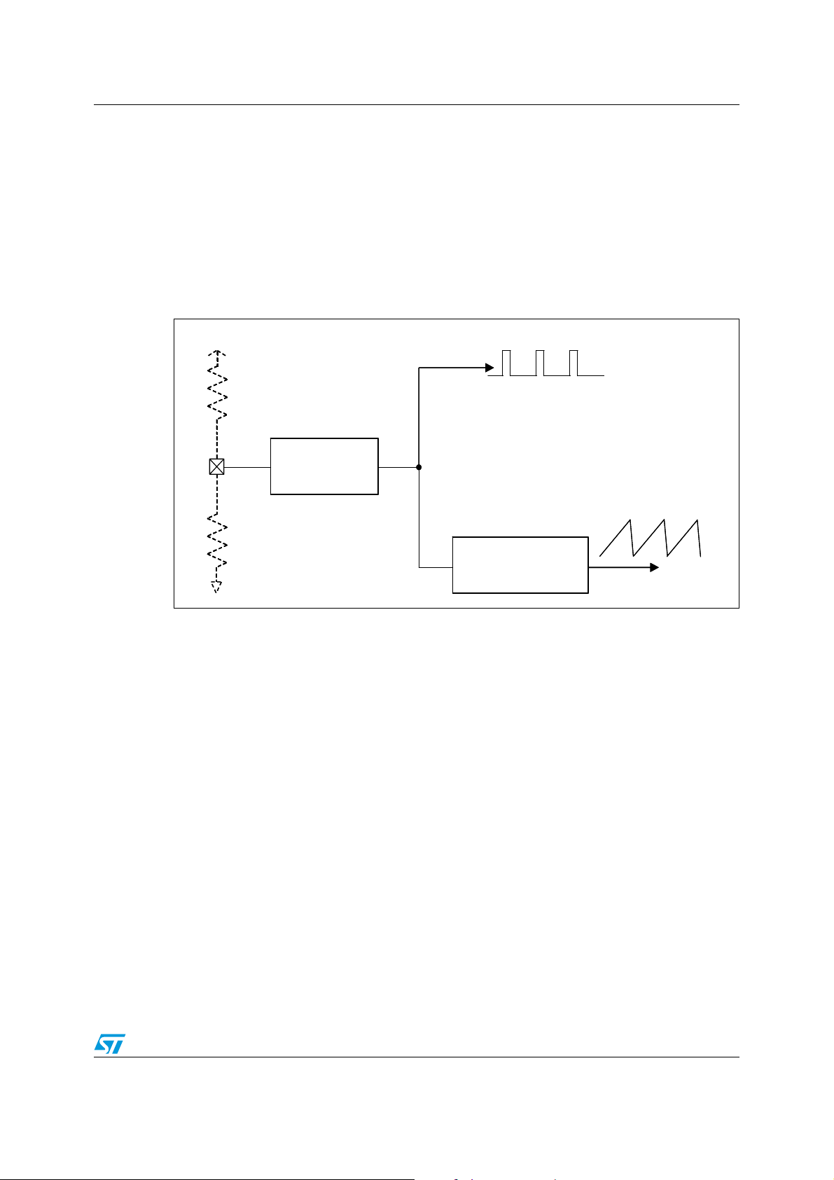
5.2 Oscillator
The generation of the internal saw-tooth waveform is based on the constant current charge /
discharge of an internal capacitor. The current generator is designed to get a switching
frequency of 400 kHz ± 10% in case the FSW pin is left floating.
The current mirror connected to FSW (see Figure 5) pin acts increasing / decreasing the
value of the internal charging current to adjust the oscillator frequency. Since the internal
circuitry forces the FSW voltage bias at 1.235 V, the user can easily source / sink current in
this pin connecting a pull up resistor to VREF or a pull down to GND respectively.
Figure 5. Oscillator circuit block diagram
VREF
VREF
Clock
ClockClock
Clock
Clock
Generator
Generator
Ramp
Ramp
Sawtooth
Generator
Generator
Sawtooth
The value of the pull up resistor versus VREF to decrease the oscillator frequency follows
the formula:
8.5 103⋅
R1KΩ()
-------------------------------------------- - 0.95+=
400 F
SW
KHz()–
In the same way to increase the switching frequency the pull down resistor is selected using
the formula:
R
2
KΩ()
18 103⋅
-------------------------------------------- - 2.1–=
KHz()400–
F
SW
Ta bl e 1 0 shows some resistor values to adjust the oscillator frequency
Doc ID 15778 Rev 3 15/51
Functional description L5989D
Table 7. FSW resistor examples
R1 (kΩ)f
(kHz) R2 (kΩ)f
SW
SW
(kHz)
43 198 360 450
47 215 180 499
56 245 120 548
62 261 91 594
82 295 56 711
110 322 43 801
150 343 33 915
220 361 27 1022
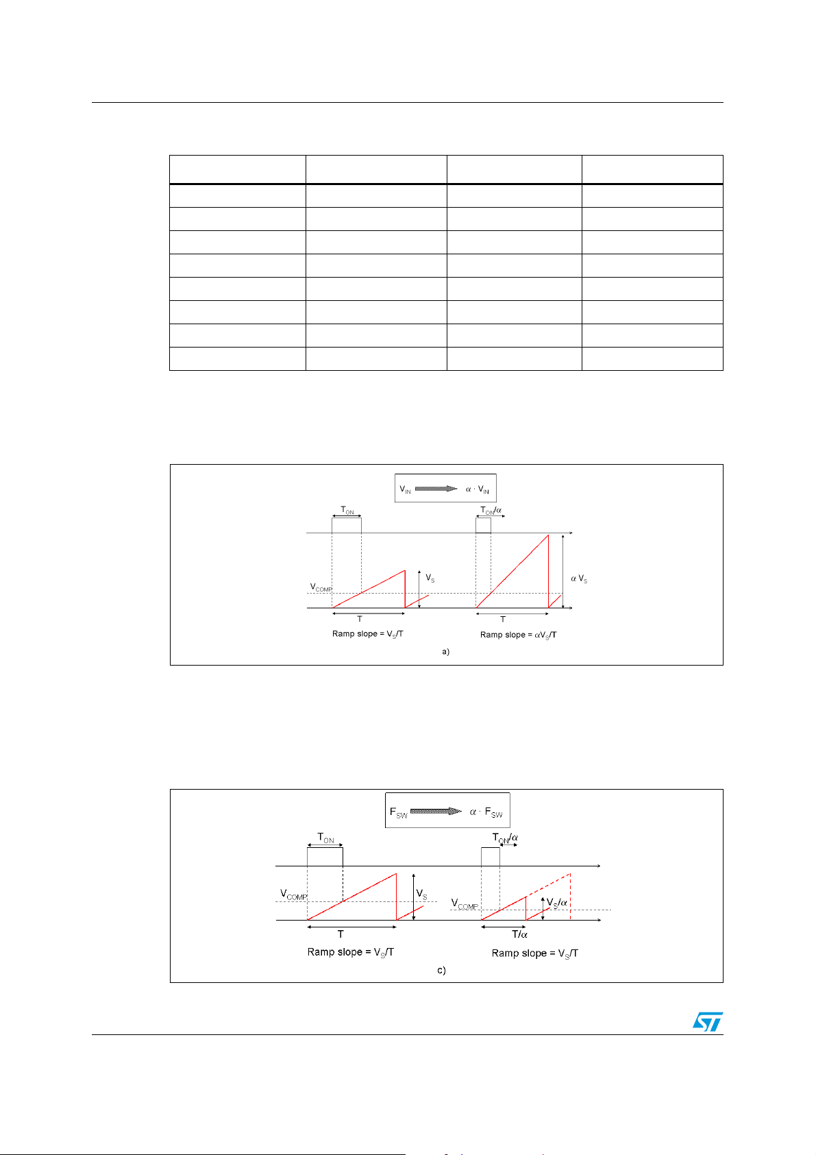
To improve the line transient performance, the voltage feed forward is implemented by
changing the slope of the sawtooth according to the input voltage change (see Figure 6 a).
Figure 6. Sawtooth: voltage feed forward
The slope of the sawtooth does not change if the oscillator frequency is increased by an
external signal or adjusted by the external resistor (see Figure 7). As a consequence the
gain of the PWM stage is a function of the switching frequency and its contribution must be
taken in account when performing the calculations of the compensation network (see
Chapter 6.4.1 and Chapter 6.4.2).
Figure 7. Sawtooth: frequency adjust
16/51 Doc ID 15778 Rev 3
 Loading...