

Features
■ 3 A DC output current
■ 2.9 V to 18 V input voltage
■ Output voltage adjustable from 0.6 V
■ 250 kHz switching frequency, programmable
up to 1 MHz
■ Internal soft-start and inhibit
■ Low dropout operation: 100% duty cycle
■ Voltage feed-forward
■ Zero load current operation
■ Over current and thermal protection
■ VFQFPN3x3-8L and HSOP8 package
Applications
■ Consumer:
STB, DVD, DVD recorder, car audio, LCD TV
and monitors
■ Industrial:
PLD, PLA, FPGA, chargers
■ Networking: XDSL, modems, DC-DC modules
■ Computer:
Optical storage, hard disk drive, printers,
audio/graphic cards
■ LED driving
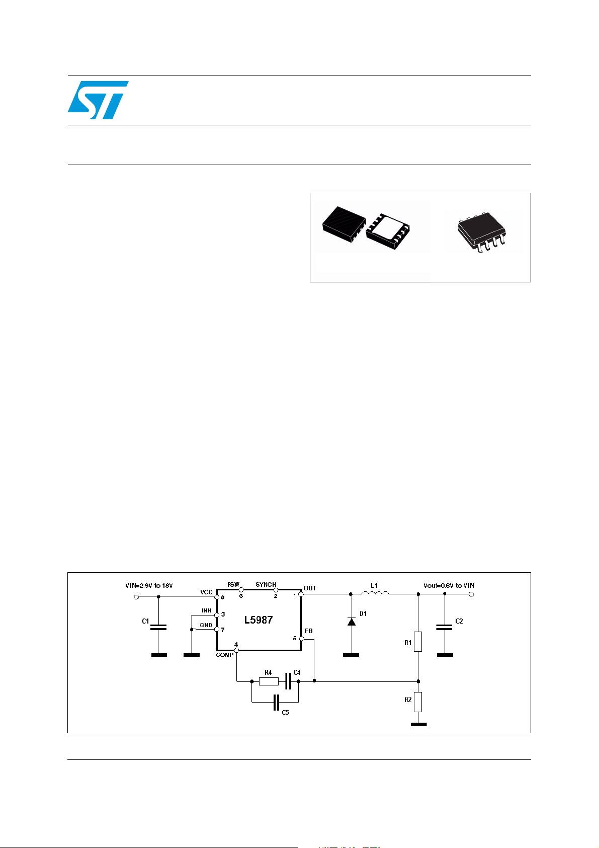
Figure 1. Application circuit
L5987
3 A step-down switching regulator
VFQFPN8 3x3 mm
Description
The L5987 is a step-down switching regulator with
3.5 A (minimum) current limited embedded power
MOSFET, so it is able to deliver up to 3 A current
to the load depending on the application
conditions (Section 5.7 and Section 5.8).
The input voltage can range from 2.9 V to 18 V,
while the output voltage can be set starting from
0.6 V to V
2.9 V, the device is suitable also for 3.3 V bus.
Requiring a minimum set of external components,
the device includes an internal 250 kHz switching
frequency oscillator that can be externally
adjusted up to 1 MHz.
The QFN and the HSOP packages with exposed
pad allow reducing the R
and 40 °C/W respectively.
. Having a minimum input voltage of
IN
HSOP8 exposed pad
down to 60 °C/W
thJA
June 2009 Doc ID 14972 Rev 3 1/41
www.st.com
41

Contents L5987
Contents
1 Pin settings . . . . . . . . . . . . . . . . . . . . . . . . . . . . . . . . . . . . . . . . . . . . . . . . 3
1.1 Pin connection . . . . . . . . . . . . . . . . . . . . . . . . . . . . . . . . . . . . . . . . . . . . . . 3
1.2 Pin description . . . . . . . . . . . . . . . . . . . . . . . . . . . . . . . . . . . . . . . . . . . . . . 3
2 Maximum ratings . . . . . . . . . . . . . . . . . . . . . . . . . . . . . . . . . . . . . . . . . . . . 4
3 Thermal data . . . . . . . . . . . . . . . . . . . . . . . . . . . . . . . . . . . . . . . . . . . . . . . 4
4 Electrical characteristics . . . . . . . . . . . . . . . . . . . . . . . . . . . . . . . . . . . . . 5
5 Functional description . . . . . . . . . . . . . . . . . . . . . . . . . . . . . . . . . . . . . . . 7
5.1 Oscillator and synchronization . . . . . . . . . . . . . . . . . . . . . . . . . . . . . . . . . . 8
5.2 Soft-start . . . . . . . . . . . . . . . . . . . . . . . . . . . . . . . . . . . . . . . . . . . . . . . . . . 10
5.3 Error amplifier and compensation . . . . . . . . . . . . . . . . . . . . . . . . . . . . . . 11
5.4 Overcurrent protection . . . . . . . . . . . . . . . . . . . . . . . . . . . . . . . . . . . . . . . 12
5.5 Inhibit function . . . . . . . . . . . . . . . . . . . . . . . . . . . . . . . . . . . . . . . . . . . . . 13
5.6 Hysteretic thermal shutdown . . . . . . . . . . . . . . . . . . . . . . . . . . . . . . . . . . 13
5.7 Maximum DC output current L5987A (HSOP8) . . . . . . . . . . . . . . . . . . . . 14
5.8 Maximum DC output current L5987 (VFQFPN) . . . . . . . . . . . . . . . . . . . . 14
6 Application information . . . . . . . . . . . . . . . . . . . . . . . . . . . . . . . . . . . . . 16
6.1 Input capacitor selection . . . . . . . . . . . . . . . . . . . . . . . . . . . . . . . . . . . . . . 16
6.2 Inductor selection . . . . . . . . . . . . . . . . . . . . . . . . . . . . . . . . . . . . . . . . . . . 17
6.3 Output capacitor selection . . . . . . . . . . . . . . . . . . . . . . . . . . . . . . . . . . . . 18
6.4 Compensation network . . . . . . . . . . . . . . . . . . . . . . . . . . . . . . . . . . . . . . 19
6.4.1 Type III compensation network . . . . . . . . . . . . . . . . . . . . . . . . . . . . . . . 20
6.4.2 Type II compensation network . . . . . . . . . . . . . . . . . . . . . . . . . . . . . . . . 24
6.5 Thermal considerations . . . . . . . . . . . . . . . . . . . . . . . . . . . . . . . . . . . . . . 28
6.6 Layout considerations . . . . . . . . . . . . . . . . . . . . . . . . . . . . . . . . . . . . . . . . 29
6.7 Application circuit . . . . . . . . . . . . . . . . . . . . . . . . . . . . . . . . . . . . . . . . . . . 31
7 Package mechanical data . . . . . . . . . . . . . . . . . . . . . . . . . . . . . . . . . . . . 35
2/41 Doc ID 14972 Rev 3

L5987 Contents
8 Order codes . . . . . . . . . . . . . . . . . . . . . . . . . . . . . . . . . . . . . . . . . . . . . . . 38
9 Revision history . . . . . . . . . . . . . . . . . . . . . . . . . . . . . . . . . . . . . . . . . . . 39
Doc ID 14972 Rev 3 3/41
Pin settings L5987
1 Pin settings
1.1 Pin connection
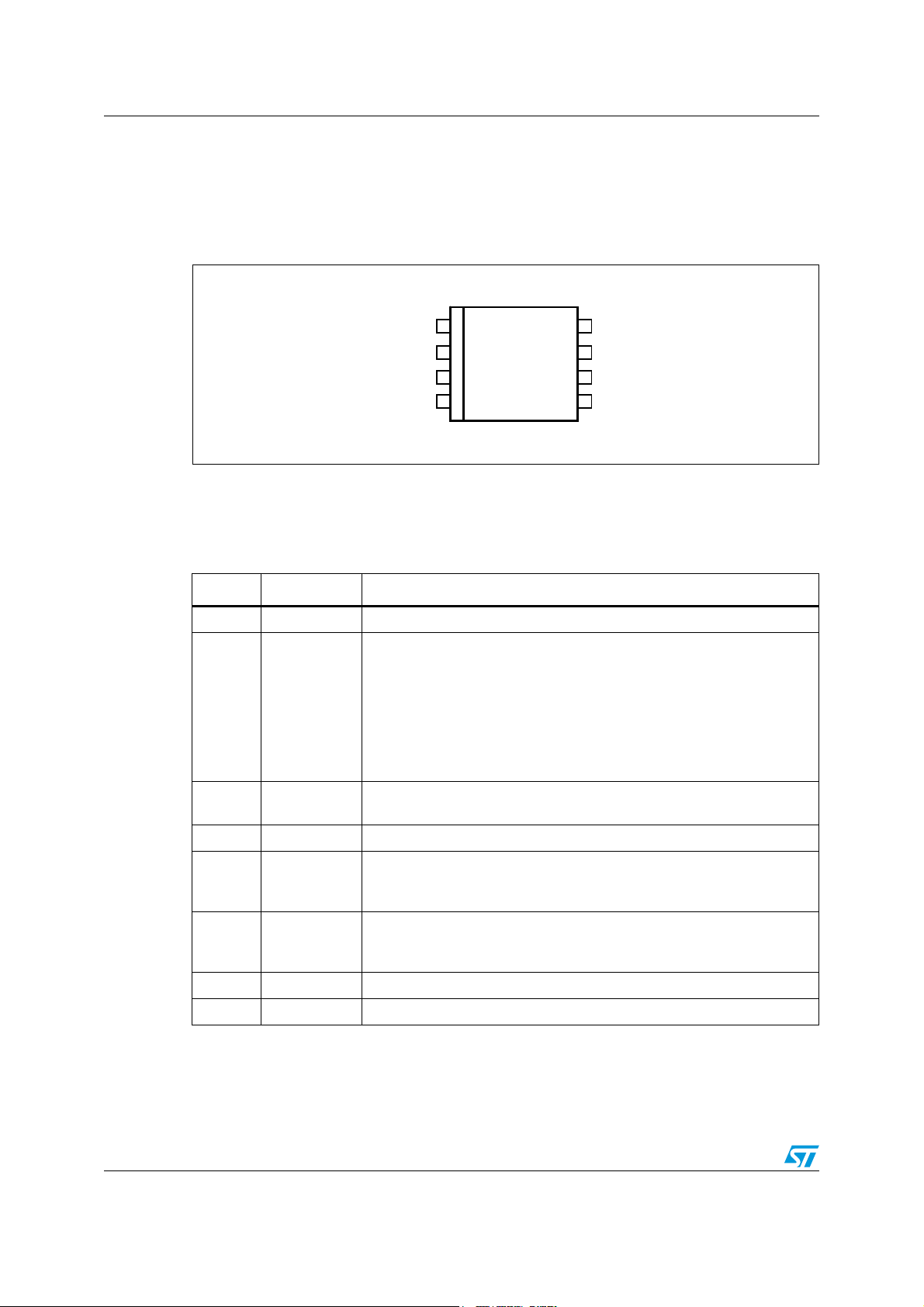
Figure 2. Pin connection (top view)
OUT
1.2 Pin description
OUT
SYNCH
SYNCH
INH
INH
COMP
COMP
V
V
CC
CC
GND
GND
FSW
FSW
FB
FB
Table 1. Pin description
N. Type Description
1 OUT Regulator output
Master/slave synchronization. When it is left floating, a signal with a
phase shift of half a period respect to the power turn on is present at the
pin. When connected to an external signal at a frequency higher than the
2 SYNCH
3INH
4 COMP Error amplifier output to be used for loop frequency compensation
5FB
6F
SW
7 GND Ground
8VCCUnregulated DC input voltage
internal one, then the device is synchronized by the external signal, with
zero phase shift.
Connecting together the SYNCH pin of two devices, the one with higher
frequency works as master and the other one as slave; so the two
powers turn on have a phase shift of half a period.
A logical signal (active high) disable the device. With INH higher than
1.9 V the device is OFF and with INH lower than 0.6 V the device is ON.
Feedback input. Connecting the output voltage directly to this pin the
output voltage is regulated at 0.6 V. To have higher regulated voltages an
external resistor divider is required from Vout to FB pin.
The switching frequency can be increased connecting an external
resistor from FSW pin and ground. If this pin is left floating the device
works at its free-running frequency of 250 kHz.
4/41 Doc ID 14972 Rev 3
L5987 Maximum ratings
2 Maximum ratings
Table 2. Absolute maximum ratings
Symbol Parameter Value Unit
Vcc Input voltage 20
OUT Output DC voltage -0.3 to V
FSW, COMP, SYNCH Analog pin -0.3 to 4
CC
V
INH Inhibit pin -0.3 to V
FB Feedback voltage -0.3 to 1.5
P
TOT
T
J
T
stg
3 Thermal data
Table 3. Thermal data
Symbol Parameter Value Unit
R
thJA
1. Package mounted on demonstration board.
CC
Power dissipation at
< 60 °C
T
A
VFQFPN 1.5. W
HSOP 2
Junction temperature range -40 to 150 °C
Storage temperature range -55 to 150 °C
Maximum thermal resistance
junction-ambient
(1)
VFQFPN 60
°C/W
HSOP 40
Doc ID 14972 Rev 3 5/41
Electrical characteristics L5987
4 Electrical characteristics
TJ = 25 °C, V
= 12 V, unless otherwise specified.
CC
Table 4. Electrical characteristics
Val ues
Symbol Parameter Test condition
Min Typ Max
V
CC
V
CCON
V
CCHYSVCC
R
DS(on)
I
LIM
Operating input voltage
range
Turn on VCC threshold
UVLO hysteresis
MOSFET on resistance
Maximum limiting current 3.5 4.0 4.4 A
Oscillator
V
F
FSW
SW
Switching frequency
FSW pin voltage 1.262 V
D Duty cycle 0 100 %
F
ADJ
Adjustable switching
frequency
(1)
(1)
(1)
2.9 18
0.175 0.3
140 170
(1)
140 220
225 250 275
(1)
= 33 kΩ 1000 kHz
R
FSW
220 265
2.9
Unit
V
mΩ
kHz
Dynamic characteristics
V
FB
Feedback voltage 2.9 V < V
CC
< 18 V
(1)
0.593 0.6 0.607 V
DC characteristics
I
Q
I
QST-BY
Quiescent current
Total stand-by quiescent
current
Duty Cycle = 0,
V
= 0.8 V
FB
2.4 mA
20 30 μA
Inhibit
Device ON level 0.6
INH threshold voltage
V
Device OFF level 1.9
INH current INH = 0 7.5 10 μA
Soft-start
T
SS
Soft-start duration
FSW pin floating 7.4 8.2 9.1
F
= 1 MHz,
R
SW
FSW
= 33 kΩ
2
ms
6/41 Doc ID 14972 Rev 3
L5987 Electrical characteristics
Table 4. Electrical characteristics (continued)
Val ues
Symbol Parameter Test condition
Min Typ Max
Error amplifier
Unit
V
CH
V
CL
I
FB
I
O SOURCE
I
O SINK
G
High level output voltage V
Low level output voltage V
Bias source current V
Source COMP pin
Sink COMP pin
Open loop voltage gain
V
Synchronization function
High input voltage 2 3.3
Low input voltage 1
Slave sink current V
Master output amplitude I
Output pulse width SYNCH floating 110
Input pulse width 70
Protection
I
FBDISC
FB disconnection source
current
Thermal shutdown 150
T
SHDN
Hysteresis 30
< 0.6 V 3
FB
> 0.6 V 0.1
FB
= 0 V to 0.8 V 1 μA
FB
= 0.5 V,
V
FB
V
COMP
= 0.7 V,
V
FB
V
COMP
(2)
SYNCH
SOURCE
= 1 V
= 1 V
= 2.9 V 0.7 0.9 mA
= 4.5 mA 2.0 V
20 mA
25 mA
100 dB
1 μA
V
V
ns
°C
1. Specification referred to TJ from -40 to +125 °C. Specification in the -40 to +125 °C temperature range are
assured by design, characterization and statistical correlation.
2. Guaranteed by design.
Doc ID 14972 Rev 3 7/41
Functional description L5987
5 Functional description
The L5987 is based on a “voltage mode”, constant frequency control. The output voltage
V
is sensed by the feedback pin (FB) compared to an internal reference (0.6 V) providing
OUT
an error signal that, compared to a fixed frequency sawtooth, controls the on and off time of
the power switch.
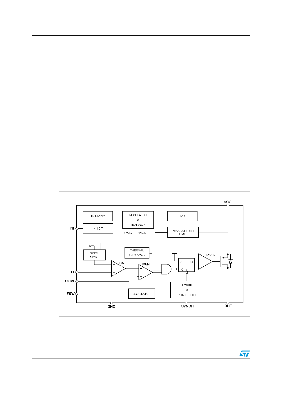
The main internal blocks are shown in the block diagram in Figure 3. They are:
● A fully integrated oscillator that provides sawtooth to modulate the duty cycle and the
synchronization signal. Its switching frequency can be adjusted by an external resistor.
The voltage and frequency feed forward are implemented.
● The soft-start circuitry to limit inrush current during the start up phase.
● The voltage mode error amplifier
● The pulse width modulator and the relative logic circuitry necessary to drive the internal
power switch.
● The High-side driver for embedded P-channel power MOSFET switch.
● The peak current limit sensing block, to handle over load and short circuit conditions.
● A voltage regulator and internal reference. It supplies internal circuitry and provides a
fixed internal reference.
● A voltage monitor circuitry (UVLO) that checks the input and internal voltages.
● A thermal shutdown block, to prevent thermal run away.
Figure 3. Block diagram
8/41 Doc ID 14972 Rev 3
L5987 Functional description
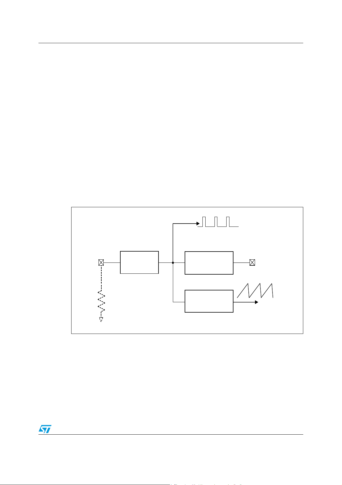
5.1 Oscillator and synchronization
Figure 4 shows the block diagram of the oscillator circuit. The internal oscillator provides a
constant frequency clock. Its frequency depends on the resistor externally connect to FSW
pin. In case the FSW pin is left floating the frequency is 250 kHz; it can be increased as
shown in Figure 6 by external resistor connected to ground.
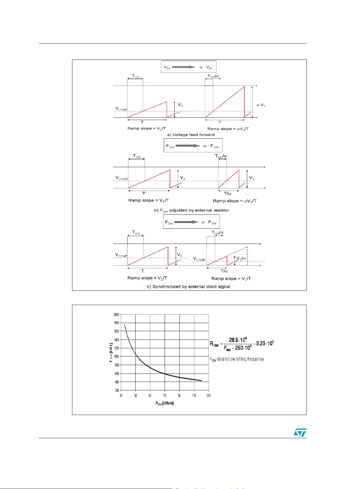
To improve the line transient performance, keeping the PWM gain constant versus the input
voltage, the voltage feed forward is implemented by changing the slope of the sawtooth
according to the input voltage change (see Figure 5.a).
The slope of the sawtooth also changes if the oscillator frequency is increased by the
external resistor. In this way a frequency feed forward is implemented (Figure 5.b) in order to
keep the PWM gain constant versus the switching frequency (see Section 6.4 for PWM gain
expression).
On the SYNCH pin the synchronization signal is generated. This signal has a phase shift of
180° with respect to the clock. This delay is useful when two devices are synchronized
connecting the SYNCH pin together. When SYNCH pins are connected, the device with
higher oscillator frequency works as Master, so the Slave device switches at the frequency
of the master but with a delay of half a period. This minimizes the RMS current flowing
through the input capacitor [see L5988D data sheet].
Figure 4. Oscillator circuit block diagram
Clock
ClockClock
FSW
FSW
Clock
Clock
Generator
Generator
Synchronization
Synchronization
Ramp
Ramp
Generator
Generator
SYNCH
SYNCH
Sawtooth
Sawtooth
The device can be synchronized to work at higher frequency feeding an external clock
signal. The synchronization changes the sawtooth amplitude, changing the PWM gain
(Figure 5.c). This changing has to be taken into account when the loop stability is studied.
To minimize the change of the PWM gain, the free running frequency should be set (with a
resistor on FSW pin) only slightly lower than the external clock frequency. This pre-adjusting
of the frequency will change the sawtooth slope in order to get negligible the truncation of
sawtooth, due to the external synchronization.
Doc ID 14972 Rev 3 9/41
Functional description L5987
Figure 5. Sawtooth: voltage and frequency feed forward; external synchronization
Figure 6. Oscillator frequency versus FSW pin resistor
10/41 Doc ID 14972 Rev 3
L5987 Functional description
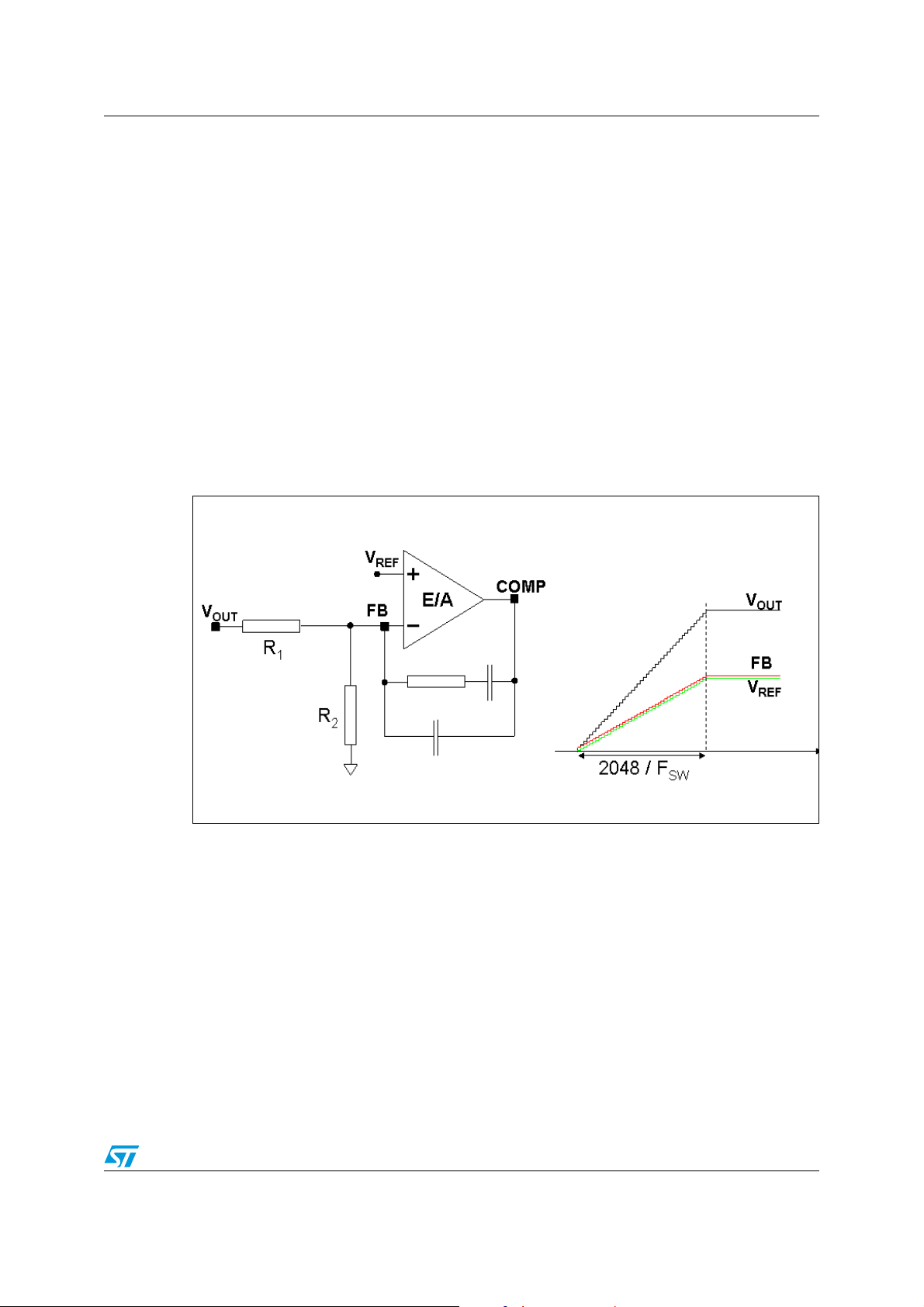
5.2 Soft-start
The soft-start is essential to assure correct and safe start up of the step-down converter. It
avoids inrush current surge and makes the output voltage increases monothonically.
The soft-start is performed by a staircase ramp on the non-inverting input (V
) of the error
REF
amplifier. So the output voltage slew rate is:
Equation 1
R1
⎛⎞
⋅=
VREF
⎝⎠
1
------- -+
R2
where SR
SR
is the slew rate of the non-inverting input, while R1and R2 is the resistor
VREF
OUT
SR
divider to regulate the output voltage (see Figure 7). The soft-start stair case consists of 64
steps of 9.5 mV each one, from 0 V to 0.6 V. The time base of one step is of 32 clock cycles.
So the soft-start time and then the output voltage slew rate depend on the switching
frequency.
Figure 7. Soft-start scheme
Soft-start time results:
Equation 2
SS
TIME
For example with a switching frequency of 250 kHz the SS
Doc ID 14972 Rev 3 11/41
32 64⋅
-----------------=
Fsw
TIME
is 8 ms.
Functional description L5987
5.3 Error amplifier and compensation
The error amplifier (E/A) provides the error signal to be compared with the sawtooth to
perform the pulse width modulation. Its non-inverting input is internally connected to a 0.6 V
voltage reference, while its inverting input (FB) and output (COMP) are externally available
for feedback and frequency compensation. In this device the error amplifier is a voltage
mode operational amplifier so with high DC gain and low output impedance.
The uncompensated error amplifier characteristics are the following:
Table 5. Uncompensated error amplifier characteristics
Parameter Value
Low frequency gain 100 dB
GBWP 4.5 MHz
Slew rate 7 V/μs
Output voltage swing 0 to 3.3 V
Maximum source/sink current 25 mA/40 mA
In continuos conduction mode (CCM), the transfer function of the power section has two
poles due to the LC filter and one zero due to the ESR of the output capacitor. Different
kinds of compensation networks can be used depending on the ESR value of the output
capacitor. In case the zero introduced by the output capacitor helps to compensate the
double pole of the LC filter a type II compensation network can be used. Otherwise, a type
III compensation network has to be used (see Chapter 6.4 for details about the
compensation network selection).
Anyway the methodology to compensate the loop is to introduce zeros to obtain a safe
phase margin.
12/41 Doc ID 14972 Rev 3

L5987 Functional description
5.4 Overcurrent protection
The L5987 implements the over-current protection sensing current flowing through the
power MOSFET. Due to the noise created by the switching activity of the power MOSFET,
the current sensing is disabled during the initial phase of the conduction time. This avoids an
erroneous detection of a fault condition. This interval is generally known as “masking time”
or “blanking time”. The masking time is about 200 ns.
When the over-current is detected, two different behaviors are possible depending on the
operating condition.
● Output voltage in regulation. When the over current is sensed, the power MOSFET is
switched off and the internal reference (V
error amplifier, is set to zero and kept in this condition for a soft-start time (T
clock cycles). After this time, a new soft-start phase takes place and the internal
reference begins ramping (see Figure 8.a).
● Soft-start phase. If the over current limit is reached the power MOSFET is turned off
implementing the pulse by pulse over current protection. During the soft-start phase,
under over current condition, the device can skip pulses in order to keep the output
current constant and equal to the current limit. If at the end of the “masking time” the
current is higher than the over current threshold, the power MOSFET is turned off and it
will skip one pulse. If, at the next switching on at the end of the “masking time” the
current is still higher than the threshold, the device will skip two pulses. This
mechanism is repeated and the device can skip up to seven pulses. While, if at the end
of the “masking time” the current is lower than the over current threshold, the number of
skipped cycles is decreased of one unit. At the end of soft-start phase the output
voltage is in regulation and if the over current persists the behavior explained above
takes place. (see Figure 8.b)
), that biases the non-inverting input of the
REF
SS
, 2048
So the over current protection can be summarized as an “hiccup” intervention when the
output is in regulation and a constant current during the soft-start phase. If the output is
shorted to ground when the output voltage is on regulation, the over current is triggered and
the device starts cycling with a period of 2048 clock cycles between “hiccup” (power
MOSFET off and no current to the load) and “constant current” with very short on-time and
with reduced switching frequency (up to one eighth of normal switching frequency). See for
short circuit behavior.
Doc ID 14972 Rev 3 13/41
 Loading...