

2.5 A switch step down switching regulator
Features
■ 2.5 A internal switch
■ Operating input voltage from 4 V to 36 V
■ 3.3 V / (±2%) reference voltage
■ Output voltage adjustable from 1.235 V to 35 V
■ Low dropout operation: 100 % duty cycle
■ 250 kHz internally fixed frequency
■ Voltage feedforward
■ Zero load current operation
■ Internal current limiting
■ Inhibit for zero current consumption
■ Synchronization
■ Protection against feedback disconnection
■ Thermal shutdown
Applications
■ Consumer: STB, DVD, TV, VCR, car radio,
LCD monitors
■ Networking: XDSL, modems, DC-DC modules
■ Computer: printers, audio/graphic cards,
optical storage, hard disk drive
■ Industrial: changers, car battery, DC-DC
converters
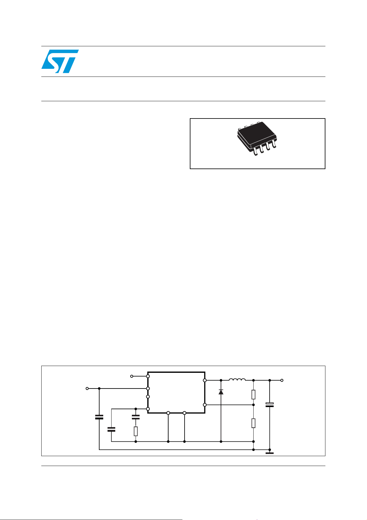
Figure 1. Test application circuit
VREF
VIN = 4.4V to 35V
C1
10µF
35V
CERAMIC
3.3V
SYNC.
COMP
C4
22nF
C3
220pF
VCC
R3
4.7K
6
8
2
4
L5973D
3
L5973D
HSOP8 exposed pad
Description
The L5973D is a step down monolithic power
switching regulator with a minimum switch current
limit of 2.5 A so it is able to deliver more than 2 A
DC current to the load depending on the
application conditions.
The output voltage can be set from 1.235 V to
35 V. The high current level is also achieved
thanks to an SO8 package with exposed frame,
that allows to reduce the Rth(j-amb) down to
approximately 40 °C/W.
The device uses an internal P-channel D-MOS
transistor (with a typical Rdson of 250 mΩ) as
switching element to minimize the size of the
external components.
An internal oscillator fixes the switching frequency
at 250 kHz.
Having a minimum input voltage of 4 V only, it is
particularly suitable for 5 V bus, available in all
computer related applications.
Pulse by pulse current limit with the internal
frequency modulation offers an effective constant
current short circuit protection.
OUT
1
5
7
GNDINH
FB
L1 15µH
D1
STPS340U
R1
5.6K
R2
3.3K
VOUT=3.3V
C2
330µF
10V
D03IN1439
January 2008 Rev 16 1/17
www.st.com
17

Contents L5973D
Contents
1 Pin settings . . . . . . . . . . . . . . . . . . . . . . . . . . . . . . . . . . . . . . . . . . . . . . . . 3
1.1 Pin connection . . . . . . . . . . . . . . . . . . . . . . . . . . . . . . . . . . . . . . . . . . . . . . 3
1.2 Pin description . . . . . . . . . . . . . . . . . . . . . . . . . . . . . . . . . . . . . . . . . . . . . . 3
2 Electrical data . . . . . . . . . . . . . . . . . . . . . . . . . . . . . . . . . . . . . . . . . . . . . . 4
2.1 Maximum ratings . . . . . . . . . . . . . . . . . . . . . . . . . . . . . . . . . . . . . . . . . . . . 4
2.2 Thermal data . . . . . . . . . . . . . . . . . . . . . . . . . . . . . . . . . . . . . . . . . . . . . . . 4
3 Electrical characteristics . . . . . . . . . . . . . . . . . . . . . . . . . . . . . . . . . . . . . 5
4 Typical characteristics . . . . . . . . . . . . . . . . . . . . . . . . . . . . . . . . . . . . . . . 7
5 Application circuit . . . . . . . . . . . . . . . . . . . . . . . . . . . . . . . . . . . . . . . . . . . 9
6 Application ideas . . . . . . . . . . . . . . . . . . . . . . . . . . . . . . . . . . . . . . . . . . . 11
7 Package mechanical data . . . . . . . . . . . . . . . . . . . . . . . . . . . . . . . . . . . . 13
8 Order code . . . . . . . . . . . . . . . . . . . . . . . . . . . . . . . . . . . . . . . . . . . . . . . . 15
9 Revision history . . . . . . . . . . . . . . . . . . . . . . . . . . . . . . . . . . . . . . . . . . . 16
2/17
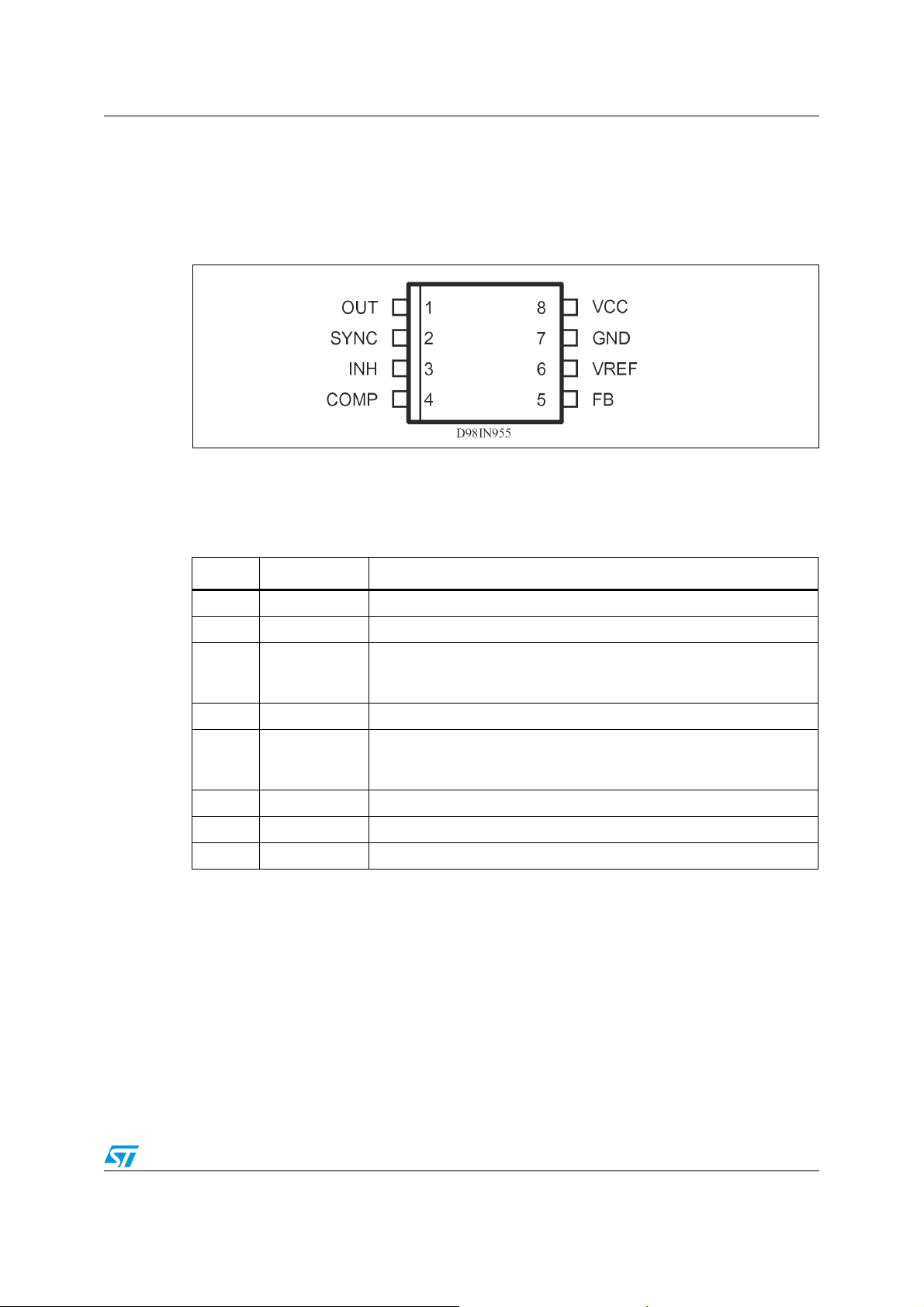
L5973D Pin settings
1 Pin settings
1.1 Pin connection
Figure 2. Pin connection (top view)
COMP
1.2 Pin description
Table 1. Pin description
N° Type Description
1 OUT Regulator output.
2 SYNC Master/slave synchronization.
3INH
4 COMP E/A output for frequency compensation.
5FB
OUT
SYNC
INH
1
2
3
4
D98IN955
A logical signal (active high) disables the device. If INH not used the pin
must be grounded. When it is open an internal pull-up disable the
device.
Feedback input. Connecting directly to this pin results in an output
voltage of 1.23 V. An external resistive divider is required for higher
output voltages.
8
7
6
5
VCC
GND
VREF
FB
6 VREF 3.3 V V
7 GND Ground.
8 VCC Unregulated DC input voltage.
. No cap is requested for stability.
REF
3/17
Electrical data L5973D
2 Electrical data
2.1 Maximum ratings
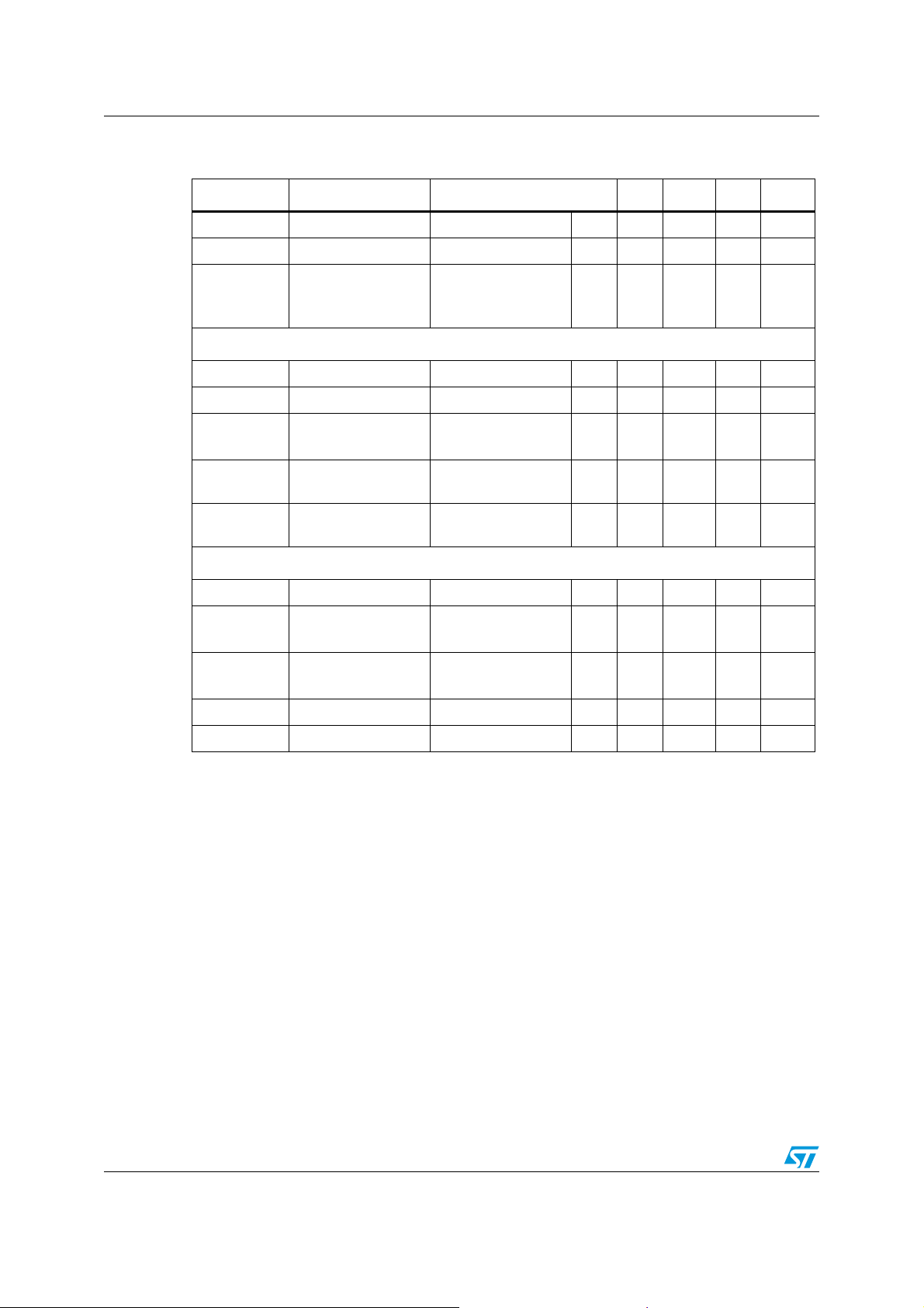
Table 2. Absolute maximum ratings
Symbol Parameter Value Unit
V
8
V
1
I
1
V
, V
4
V
3
V
2
P
TOT
T
J
T
STG
Input voltage 40 V
Output DC voltage
Output peak voltage at t = 0.1 µs
Maximum output current int. limit.
Analog pins 4 V
5
INH -0.3 V to V
SYNC -0.3 to 4 V
Power dissipation at TA ≤ 60 °C 2.25 W
Operating junction temperature range -40 to 150 °C
Storage temperature range -55 to 150 °C
2.2 Thermal data
Table 3. Thermal data
Symbol Parameter
R
thJA
1. Package mounted on board
Maximum thermal resistance junction-ambient 40
-1 to 40
-5 to 40
CC
HSOP8
Exposed Pad
(1)
V
V
Unit
°C/W
4/17
L5973D Electrical characteristics
3 Electrical characteristics
Table 4. Electrical characteristics
( TJ = 25 °C, VCC = 12 V, unless otherwise specified)
Symbol Parameter Test condition Min Typ Max Unit
V
R
DS(on)
f
CC
I
s
l
Operating input
voltage range
Mosfet on
Resistance
Maximum limiting
current
Switching frequency
= 1.235 V; Io = 2 A
V
o
V
CC
Duty cycle 0 100 %
Dynamic characteristics (see test circuit ).
V
5
Voltage feedback
h Efficiency V
4.4 V < V
20 mA < I
= 5 V, VCC = 12 V 90 %
O
DC characteristics
I
qop
I
I
qst-by
q
Total operating
quiescent current
Quiescent current
Total stand-by
quiescent current
Duty Cycle = 0;
V
FB
V
inh
V
CC
V
inh
Inhibit
(1)
(1)
436V
0.250 0.5 Ω
= 4.4 V to 36 V 2.5 3 3.5 A
(1)
212 250 280 kHz
225 250 275 kHz
CC
O
= 1.5 V
> 2.2 V
= 36 V;
> 2.2 V
< 36 V,
< 2 A
1.220 1.235 1.25 V
(1)
1.198 1.235 1.272 V
(1)
(1)
(1)
35mA
50 100 µA
80 150 µA
2.5 mA
Error amplfier
V
OH
V
OL
I
o source
I
o sink
INH threshold
voltage
High level output
voltage
Low level output
voltage
Source output
current
Sink output current
Device ON 0.8 V
Device OFF 2.2 V
VFB = 1 V 3.5 V
VFB = 1.5 V 0.4 V
V
= 1.9 V;
COMP
= 1 V
V
FB
= 1.9 V;
V
COMP
VFB = 1.5 V
200 300 µA
11.5 mA
5/17
Electrical characteristics L5973D
Table 4. Electrical characteristics (continued)
( TJ = 25 °C, VCC = 12 V, unless otherwise specified)
Symbol Parameter Test condition Min Typ Max Unit
I
b
Source bias current 2.5 4 µA
DC open loop gain R
gm Transconductance
Sync function
High input voltage V
Low input voltage V
Slave sink current
Master output
amplitude
Output pulse width
Reference section
Reference voltage 3.234 3.3 3.366 V
Line regulation
Load regulation I
Short circuit current 10 18 30 mA
= ∞ 50 57 dB
L
= -0.1 mA to
I
comp
0.1 mA
= 1.9 V
V
COMP
= 4.4 V to 36 V 2.5 V
CC
= 4.4 V to 36 V 0.74 V
CC
= 0.74 V
V
sync
V
= 2.33 V
sync
= 3 mA 2.75 3 V
I
source
(2)
no load,
V
= 1.65 V
sync
I
= 0 to 5 mA
REF
= 4.4 V to 36 V
V
CC
I
= 0 mA
REF
= 4.4 V to 36 V
V
CC
= 0 to 5 mA 8 15 mV
REF
0.11
0.21
0.20 0.35 µs
(1)
3.2 3.3 3.399 V
2.3 mS
REF
0.25
0.45mAmA
510mV
V
1. Specification Referred to TJ from -40 to 125 °C. Specification over the -40 to +125 TJ Temperature range
are assured by design, characterization and statistical correlation.
2. Guaranteed by design.
6/17

L5973D Typical characteristics
4 Typical characteristics
Figure 3. Line regulation Figure 4. Shutdown current vs junction
Vo (V)
3.312
Vcc = 12V
3.308
Vo = 3.3V
3.304
3.3
3.296
3.292
3.288
3.284
3.28
3.276
010203040
Tj = 25°C
Tj = 125°C
Vcc (V)
Ishd (µA)
70
60
50
40
30
-50
temperature
Vcc = 12V
0
50 100 150
Tj (°C)
Figure 5. Output voltage vs junction
Vo (V)
1.25
1.24
1.23
1.22
1.21
1.2
-50 0 50 100 150
temperature
Vcc = 12V
Vcc=12V
Tj (°C)
Figure 7. Quiescent current vs junction
Iq (mA)
2
1.8
temperature
Figure 6. Switching frequency vs
junction temperature
Fsw (KHz)
260
250
240
230
220
-50 0 50 100 150
Vcc = 12V
Vo = 3.3V
Tj (°C)
1.6
1.4
1.2
-50
Vcc = 12V
DC = 0%
050
Tj (°C)
100 150
7/17

Typical characteristics L5973D
Figure 8. Junction temperature vs
Tj(°C)
120
110
100
90
80
70
60
50
40
30
20
0.2 0.4 0.6 0.8 1 1.2 1.4 1.6 1.8 2 2.2 2.4 2.6
Figure 10. Efficiency vs output current Figure 11. Efficiency vs output current
output current
Vin=5V
Tamb=25°C
Io(A)
Vo=3.3V
Vo=2.5V
Vo=1.8V
Figure 9. Junction temperature vs
output current
Tj (°C)
120
110
Vin=12V
100
Tamb=25°C
90
80
70
60
50
40
30
20
0.2 0.4 0.6 0.8 1 1.2 1.4 1.6 1.8 2 2.2 2.4 2.6
Io (A)
Vo=5V
Vo=2.5V
Vo=3.3V
95
93
91
89
87
85
83
81
79
77
Efficiency (%)
75
73
71
69
67
0.1 0.3 0.5 0.7 0.9 1.1 1.3 1.5 1.7 1.9 2.1 2.3
Vo=2.5V
Vo=1.8V
Vin=5V
Vo=3.3V
Io (A)
91
89
87
85
83
81
79
77
75
Efficiency (%)
73
71
Vin=12V
69
67
65
0.1 0.3 0.5 0.7 0.9 1.1 1.3 1.5 1.7 1.9 2.1 2.3
Vo=5V
Vo=3.3V
Vo=2.5V
Io (A)
8/17

L5973D Application circuit
5 Application circuit
In figure 6 is shown the demonstration board application circuit, where the input supply
voltage, V
the output voltage is adjustable from 1.235 V to V
Figure 12. Demonstration board application circuit
, can range from 4 V to 25 V due to the rated voltage of the input capacitor and
CC
CC
.
VIN = 4.4V to 25V
C1
10µF
25V
CERAMIC
3.3V
C4
22nF
C3
220pF
VREF
VCC
SYNC.
COMP
R3
4.7K
6
8
2
4
L5973D
3
7
GNDINH
D03IN1440
OUT
1
5
FB
L1 15µH
D1
STPS2L25U
R1
5.6K
R2
3.3K
Table 5. Component list
Reference Part number Description Manufacturer
C1 GRM32DR61E106KA12L 10 µF, 25 V Murata
C2 POSCAP 6TPB330M 330 µF, 6.3 V Sanyo
C3 C1206C221J5GAC 220 pF, 5%, 50 V KEMET
C4 C1206C223K5RAC 22 nF, 10%, 50 V KEMET
R1 5.6 K, 1%, 0.1 W 0603 Neohm
VOUT=3.3V
C2
330µF
6.3V
R2 3.3 K, 1%, 0.1 W 0603 Neohm
R3 4.7 K, 1%, 0.1 W 0603 Neohm
D1 STPS2L25U 2 A, 25 V ST
L1 DO3316P-153 15 µH, 3 A COILCRAFT
9/17

Application circuit L5973D
Figure 13. PCB layout (component side)
Figure 14. PCB layout (bottom side)
Figure 15. PCB layout (front side)
Below some graphs show the T
versus output current in different conditions of the input and
J
output voltage and some efficiency measurements.
10/17

L5973D Application ideas
6 Application ideas
Figure 16. Positive buck-boost regulator
Figure 17. Buck-boost regulator
Figure 18. Dual output voltage with auxiliary winding
11/17

Application ideas L5973D
When an output voltage below the internal reference (1.235 V) is required, the circuit
reported in the figure 18 can been used. In this case the minimum voltage reachable is 0.6 V
and can be easily calculated with the following formula:
V
= V
OUT
FB
- [(V
If the load is not present, a resistor connected between V
to avoid that the voltage across C
- VFB)x(R2 / R1)]
REF
increases.
OUT
and GND is required in order
OUT
The value of this resistor has to be calculated taking into account that the current flowing
through this resistance has to be higher than the current flowing through R
.
2
Figure 19. Output voltage below the 1.235 V internal voltage reference
12/17

L5973D Package mechanical data
7 Package mechanical data
In order to meet environmental requirements, ST offers these devices in ECOPACK®
packages. These packages have a Lead-free second level interconnect . The category of
second level interconnect is marked on the package and on the inner box label, in
compliance with JEDEC Standard JESD97. The maximum ratings related to soldering
conditions are also marked on the inner box label. ECOPACK is an ST trademark.
ECOPACK specifications are available at: www.st.com
13/17

Package mechanical data L5973D
Table 6. HSOP8 mechanical data
mm inch
Dim
Min Typ Max Min Typ Max
A 1.70 0.0669
A1 0.00 0.10 0.00 0.0039
A2 1.25 0.0492
b 0.31 0.51 0.0122 0.0201
c 0.17 0.25 0.0067 0.0098
D 4.80 4.90 5.00 0.1890 0.1929 0.1969
D1 3 3.1 3.2 0.118 0.122 0.126
E 5.80 6.00 6.20 0.2283 0.2441
E1 3.80 3.90 4.00 0.1496 0.1575
E2 2.31 2.41 2.51 0.091 0.095 0.099
e1.27
h 0.25 0.50 0.0098 0.0197
L 0.40 1.27 0.0157 0.0500
k0° (min), 8° (max)
ccc 0.10 0.0039
Figure 20. Package dimensions
14/17
L5973D Order code
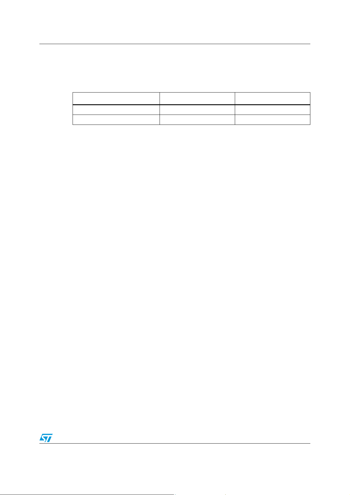
8 Order code
Table 7. Order code
Part number Package Packaging
L5973D HSOP8 (Exposed pad) Tube
L5973D013TR HSOP8 (Exposed pad) Tape and reel
15/17

Revision history L5973D
9 Revision history
pp
Table 8. Revision history
Date Revision Changes
01-Nov-2005 10 Updated package information
22-May-2006 11
13-Nov-2006 12 Typo in order codes
26-Jan-2007 13 Updated Table 4 on page 5
17-Oct-2007 14 Updated Section 5: Application circuit on page 9
24-Oct-2007 15 Updated Table 6 on page 14
07-Jan-2008 16 Updated Table 6 on page 14
Electrical characteristic Tab l e 4 updated, new application idea
Figure 19 added, new template
16/17

L5973D
Please Read Carefully:
Information in this document is provided solely in connection with ST products. STMicroelectronics NV and its subsidiaries (“ST”) reserve the
right to make changes, corrections, modifications or improvements, to this document, and the products and services described herein at any
time, without notice.
All ST products are sold pursuant to ST’s terms and conditions of sale.
Purchasers are solely responsible for the choice, selection and use of the ST products and services described herein, and ST assumes no
liability whatsoever relating to the choice, selection or use of the ST products and services described herein.
No license, express or implied, by estoppel or otherwise, to any intellectual property rights is granted under this document. If any part of this
document refers to any third party products or services it shall not be deemed a license grant by ST for the use of such third party products
or services, or any intellectual property contained therein or considered as a warranty covering the use in any manner whatsoever of such
third party products or services or any intellectual property contained therein.
UNLESS OTHERWISE SET FORTH IN ST’S TERMS AND CONDITIONS OF SALE ST DISCLAIMS ANY EXPRESS OR IMPLIED
WARRANTY WITH RESPECT TO THE USE AND/OR SALE OF ST PRODUCTS INCLUDING WITHOUT LIMITATION IMPLIED
WARRANTIES OF MERCHANTABILITY, FITNESS FOR A PARTICULAR PURPOSE (AND THEIR EQUIVALENTS UNDER THE LAWS
OF ANY JURISDICTION), OR INFRINGEMENT OF ANY PATENT, COPYRIGHT OR OTHER INTELLECTUAL PROPERTY RIGHT.
UNLESS EXPRESSLY APPROVED IN WRITING BY AN AUTHORIZED ST REPRESENTATIVE, ST PRODUCTS ARE NOT
RECOMMENDED, AUTHORIZED OR WARRANTED FOR USE IN MILITARY, AIR CRAFT, SPACE, LIFE SAVING, OR LIFE SUSTAINING
APPLICATIONS, NOR IN PRODUCTS OR SYSTEMS WHERE FAILURE OR MALFUNCTION MAY RESULT IN PERSONAL INJURY,
DEATH, OR SEVERE PROPERTY OR ENVIRONMENTAL DAMAGE. ST PRODUCTS WHICH ARE NOT SPECIFIED AS "AUTOMOTIVE
GRADE" MAY ONLY BE USED IN AUTOMOTIVE APPLICATIONS AT USER’S OWN RISK.
Resale of ST products with provisions different from the statements and/or technical features set forth in this document shall immediately void
any warranty granted by ST for the ST product or service described herein and shall not create or extend in any manner whatsoever, any
liability of ST.
ST and the ST logo are trademarks or registered trademarks of ST in various countries.
Information in this document supersedes and replaces all information previously supplied.
The ST logo is a registered trademark of STMicroelectronics. All other names are the property of their respective owners.
© 2008 STMicroelectronics - All rights reserved
STMicroelectronics group of companies
Australia - Belgium - Brazil - Canada - China - Czech Republic - Finland - France - Germany - Hong Kong - India - Israel - Italy - Japan -
Malaysia - Malta - Morocco - Singapore - Spain - Sweden - Switzerland - United Kingdom - United States of America
www.st.com
17/17
 Loading...