

Features
■ L5958 six outputs:
– 8.5 V @ 200 mA
– 5.0 V @ 300 mA
– 3.3 V @ 250 mA
– 1.8 V @ 350 mA
– 3.3 V @ 100 mA standby
– 1.8 V @ 100 mA standby
■ 2 A high side driver
■ Reset function
■ VDD core reset function
■ Battery audio warning
■ Battery can warning
■ Ignition comparator
■ Load dump protection
■ Thermal shutdown
■ Overcurrent limitation
■ All pin ESD protected
L5958
Multifunction voltage regulator for car radio
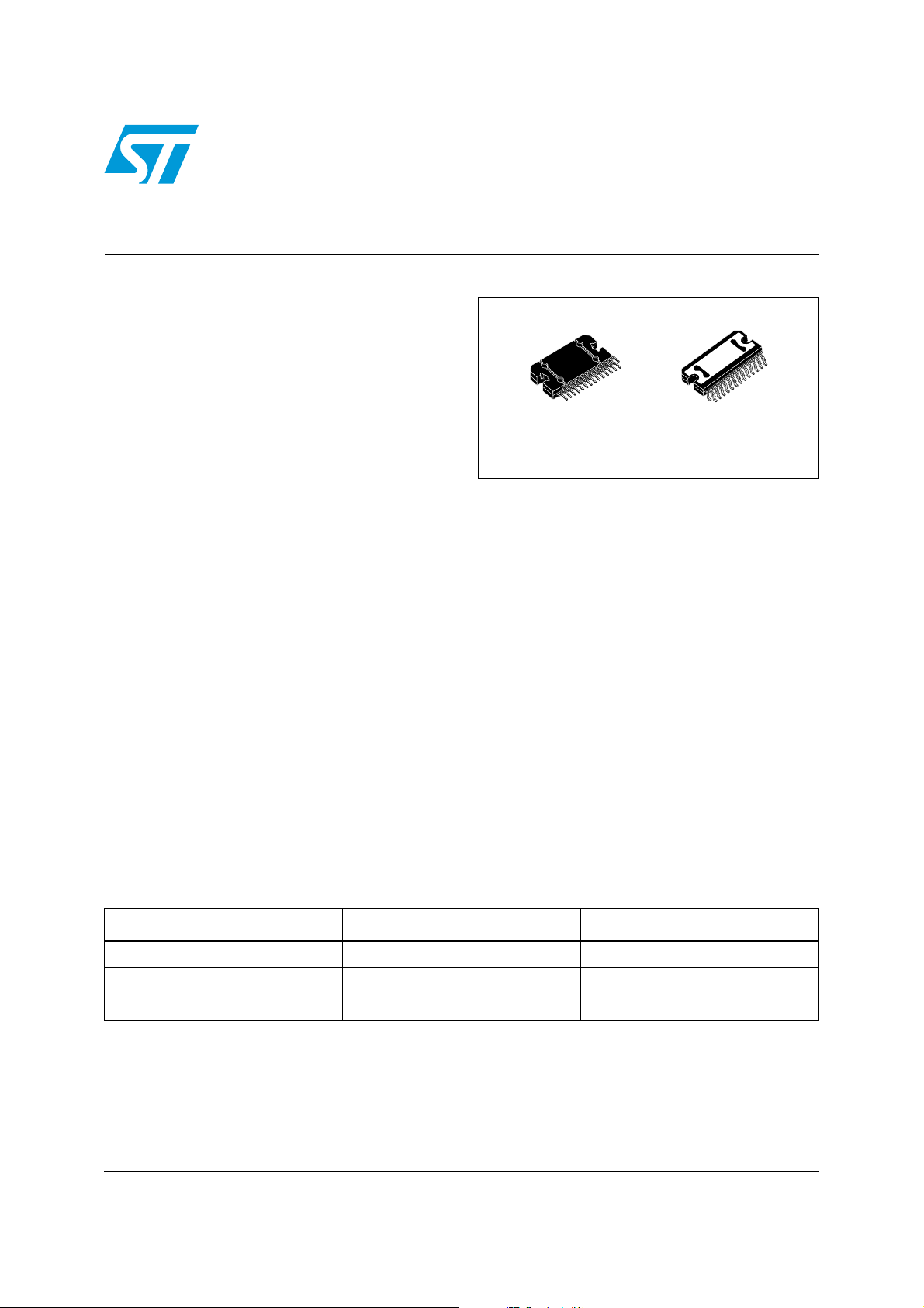
Flexiwatt27
(vertical)
The two 3.3 V (REG5) and 1.8 V (REG6) stand-by
regulators can reach a quasi-zero current
consumption when switched off.
The device is equipped with two different reset
buffers to control the operating voltages: the reset
which checks the two stand-by outputs, 3.3V and
1.8 V, and the VDD core reset which checks the
linear switched outputs, 3.3 V and 1.8 V. It is also
equipped with two different battery voltage
warnings, provided by the Hold CAN and the Hold
audio detectors, with the possibility to program
the lower threshold through an external
resistance.
Flexiwatt27
(SMD)
Description
The L5958 includes 6 linear voltage regulators
and a 2 A power switch, working down to 4.5 V
battery level. All the voltage regulators can be
switched off through the three enable pins.
Table 1. Device summary
Order code Package Packing
L5958 Flexiwatt27 (vertical) Tube
L5958SM Flexiwatt27 (SMD) Tube
L5958SMTR Flexiwatt27 (SMD) Tape and reel
July 2010 Doc ID 17716 Rev 1 1/20
The ignition buffer completes the device.
A backup function is available through two pins
which needs to be connected to two independent
capacitors: one for the 3.3 V and 1.8 V linear
switched outputs and one for the 3.3 V and 1.8 V
standby outputs.
www.st.com
1

Contents L5958
Contents
1 Block diagram . . . . . . . . . . . . . . . . . . . . . . . . . . . . . . . . . . . . . . . . . . . . . . 5
2 Pin description . . . . . . . . . . . . . . . . . . . . . . . . . . . . . . . . . . . . . . . . . . . . . 6
3 Electrical specifications . . . . . . . . . . . . . . . . . . . . . . . . . . . . . . . . . . . . . . 8
3.1 Absolute maximum ratings . . . . . . . . . . . . . . . . . . . . . . . . . . . . . . . . . . . . . 8
3.2 Thermal data . . . . . . . . . . . . . . . . . . . . . . . . . . . . . . . . . . . . . . . . . . . . . . . 8
3.3 Electrical characteristics . . . . . . . . . . . . . . . . . . . . . . . . . . . . . . . . . . . . . . . 8
3.4 Application diagram . . . . . . . . . . . . . . . . . . . . . . . . . . . . . . . . . . . . . . . . . 12
3.5 Timing diagrams . . . . . . . . . . . . . . . . . . . . . . . . . . . . . . . . . . . . . . . . . . . . 14
4 Package information . . . . . . . . . . . . . . . . . . . . . . . . . . . . . . . . . . . . . . . . 17
5 Revision history . . . . . . . . . . . . . . . . . . . . . . . . . . . . . . . . . . . . . . . . . . . 19
2/20 Doc ID 17716 Rev 1

L5958 List of tables
List of tables
Table 1. Device summary . . . . . . . . . . . . . . . . . . . . . . . . . . . . . . . . . . . . . . . . . . . . . . . . . . . . . . . . . . 1
Table 2. Pin description . . . . . . . . . . . . . . . . . . . . . . . . . . . . . . . . . . . . . . . . . . . . . . . . . . . . . . . . . . . 7
Table 3. Absolute maximum ratings . . . . . . . . . . . . . . . . . . . . . . . . . . . . . . . . . . . . . . . . . . . . . . . . . . 8
Table 4. Thermal data. . . . . . . . . . . . . . . . . . . . . . . . . . . . . . . . . . . . . . . . . . . . . . . . . . . . . . . . . . . . . 8
Table 5. Electrical characteristics . . . . . . . . . . . . . . . . . . . . . . . . . . . . . . . . . . . . . . . . . . . . . . . . . . . . 8
Table 6. Document revision history . . . . . . . . . . . . . . . . . . . . . . . . . . . . . . . . . . . . . . . . . . . . . . . . . 19
Doc ID 17716 Rev 1 3/20

List of figures L5958
List of figures
Figure 1. Block diagram . . . . . . . . . . . . . . . . . . . . . . . . . . . . . . . . . . . . . . . . . . . . . . . . . . . . . . . . . . . . 5
Figure 2. Flexiwatt27 (SMD and vertical) pin connection (top view) . . . . . . . . . . . . . . . . . . . . . . . . . . 6
Figure 3. Application circuit . . . . . . . . . . . . . . . . . . . . . . . . . . . . . . . . . . . . . . . . . . . . . . . . . . . . . . . . 12
Figure 4. Regulator and power switch diagram . . . . . . . . . . . . . . . . . . . . . . . . . . . . . . . . . . . . . . . . . 13
Figure 5. Timing chart V
Figure 6. Timing chart 1.8 Vperm/3.3 Vperm and 1.8V sw/3.3 Vsw . . . . . . . . . . . . . . . . . . . . . . . . . 14
Figure 7. Reset and BU1 backup diagram . . . . . . . . . . . . . . . . . . . . . . . . . . . . . . . . . . . . . . . . . . . . . 15
Figure 8. BU2 backup diagram . . . . . . . . . . . . . . . . . . . . . . . . . . . . . . . . . . . . . . . . . . . . . . . . . . . . . 15
Figure 9. Maximum ESR for stability (valid for all the regulator outputs) . . . . . . . . . . . . . . . . . . . . . . 15
Figure 10. Current limit of the power switch. . . . . . . . . . . . . . . . . . . . . . . . . . . . . . . . . . . . . . . . . . . . . 16
Figure 11. Flexiwatt27 (vertical) mechanical data and package dimensions . . . . . . . . . . . . . . . . . . . . 17
Figure 12. Flexiwatt27 (SMD) mechanical data and package dimensions . . . . . . . . . . . . . . . . . . . . . 18
detection . . . . . . . . . . . . . . . . . . . . . . . . . . . . . . . . . . . . . . . . . . . . . . . . 14
batt
4/20 Doc ID 17716 Rev 1
L5958 Block diagram
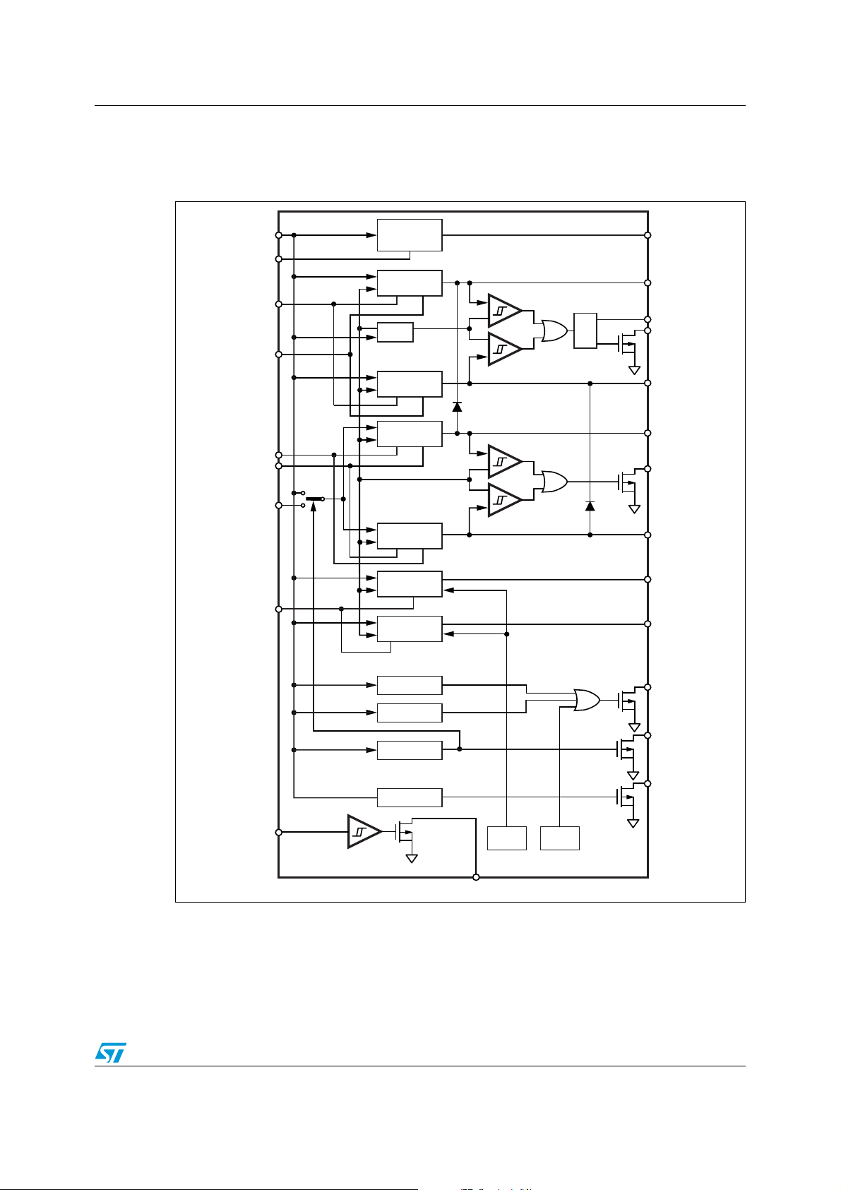
1 Block diagram
Figure 1. Block diagram
VIN1
EN_SW
EN_3P3P -1P8P
BU1
EN_3P3SW_1P8SW
EN_8P5SW_5PSW
BU2
V IN2
POWER
SWITCH
1.8V perm
REGULATOR
V
ref
3.3V perm
REGULATOR
1.8V
REGULATOR
3.3V
REGULATOR
5V
REGULATOR
8.5V
REGULATOR
RES
BUF
SW
REG6
CRES
RES
REG5
REG4
VDD CORE
REG3
REG2
REG1
IGNIN
<5.37V
>18.55V
<8.65V
>16.55V
IGNOUT
LOAD
DUMP
PRE
WARN
CAN_PRETEMP
AUDIO_LOW_OUT
AUDIO_HIGH_OUT
AC00175
Doc ID 17716 Rev 1 5/20
Pin description L5958
2 Pin description
Figure 2. Flexiwatt27 (SMD and vertical) pin connection (top view)
SMD
Vertical
1
2
3
4
5
6
7
8
9
10
11
12
13
14
15
16
17
18
19
20
21
22
23
24
25
26
27
27
26
25
24
23
22
21
20
19
18
17
16
15
14
13
12
11
10
9
8
7
6
5
4
3
2
1
TAB
REG6(1P8P)
RES
BU1
CRES
REG5(3P3P)
GND
SW
EN_SW
AUDIO_LOW_IN
VDDCORE
VIN1
CAN_LOW_IN
AUDIO_HIGH_OUT
AUDIO_LOW_OUT
REG2(5V)
CAN_PRETEMP
REG1(8P5)
EN_8P5_5
REG4(1P8sw)
IGNOUT
VIN2
IGNIN
REG3((3P3sw)
EN_3P3_1P8
BU2
EN_3P3sw_1P8sw
D06AU1652B
EN_3P3sw_1P8sw
BU2
EN_3P3_1P8
REG3((3P3sw)
IGNIN
VIN2
IGNOUT
REG4(1P8sw)
EN_8P5_5
REG1(8P5)
CAN_PRETEMP
REG2(5V)
AUDIO_LOW_OUT
AUDIO_HIGH_OUT
CAN_LOW_IN
VIN1
VDDCORE
AUDIO_LOW_IN
EN_SW
SW
GND
REG5(3P3P)
CRES
BU1
RES
REG6(1P8P)
TAB
6/20 Doc ID 17716 Rev 1

L5958 Pin description
Table 2. Pin description
Pin N# Pin name Function Type
1TAB
2 REG6(1P8P) Output of Reg6 (1.8 V/100 mA) O
3 RES Reset signal for MCU application O
Connect to a reserve capacitor. When battery is
4BU1
5 CRES Connect a capacitor to delay reset signal O
6 REG5(3P3P) Output of Reg5 (3.3 V/100 mA) O
7 GND Power supply ground S
8 SW Output of power switch O
9 EN_SW Enable signal for SW I
10 AUDIO_LOW_IN Hold Audio Low threshold adjustment I
11 VDDCORE Warn signal to 3.3 Vsw or 1. 8Vsw O
12 VIN1 Power supply for Reg1,Reg2,Reg5,Reg6 and SW S
13 CAN_LOW_IN Hold CAN Low threshold adjustment I
14 AUDIO_HIGH_OUT Hold Audio High signal for MCU application O
removed suddenly, the energy stored in this
capacitor can still supply reg5 and reg6 for some
time.
I/O
15 AUDIO_LOW_OUT Hold Audio Low signal for MCU application O
16 REG2(5V) Output of Reg2 O
17 CAN_PRETEMP
Hold can low signal or hold can high signal with
load dump detection or pretemp warning
18 REG1(8P5) Output of Reg1 O
19 EN_8P5_5 Enable signal for 5 V and 8.5 V I
20 REG4(1P8sw) Output of Reg4 (1.8 V/350 mA) O
21 IGNOUT Ignition signal output O
22 VIN2 Power supply for Reg3 and Reg4 S
23 IGNIN Ignition signal input I
24 REG3((3P3sw) Output of Reg3 (3.3 V / 250 mA) O
Enable signal for 3.3 Vperm and 1.8 Vperm.
25 EN_3P3_1P8
A resistor of 1 kΩ in series to this control pin is
suggested.
Connect to a reserve capacitor. When battery is
26 BU2
removed suddenly, the energy stored in this
capacitor can still supply reg3 and reg4 for some
I/O
time.
27 EN_3P3sw_1P8sw Enable signal for 3.3 V and 1.8 V I
O
I
Doc ID 17716 Rev 1 7/20

Electrical specifications L5958
3 Electrical specifications
3.1 Absolute maximum ratings
Table 3. Absolute maximum ratings
Symbol Parameter Value Unit
V
DC operating supply voltage 30 V
SDC
Transient supply voltage 50 V
V
STR
Output current internally limited
I
O
T
T
T
V
pinMIN
Operating temperature range -40 to 105 °C
op
Storage temperature -55 to 150 °C
stg
Junction temperature -55 to 150 °C
j
Minimum pin voltage (EN_SW, AUDIO_LOW_IN,
CAN_LOW_IN, EN_8P5_5, IGNIN, EN_3P3_1P8,
-0.3 V
EN_3P3sw_1P8sw)
3.2 Thermal data
Table 4. Thermal data
Symbol Parameter Value Unit
R
Thermal resistance junction-to-case Max. 1.0 °C/W
th j-case
3.3 Electrical characteristics
VS = 14.4 V; T
Table 5. Electrical characteristics
Symbol Parameter Test condition Min. Typ. Max. Unit
Input supplies
V
V
V
V
Input supply voltage 1 Operating 9 - 18 V
in1
Input supply voltage 2 Operating 4.5 - 18 V
in2
Input supply voltage 1 Reverse polarity - not operating -
in1
Input supply voltage 2 Reverse polarity - not operating -
in2
I
Total quiescent current
q
= 25 °C; unless otherwise specified
amb
Standby (-40 °C to 85 °C)
Perm reg on
Standby (25 °C) Perm reg off - 4 10 µA
Standby (-40 °C to 85 °C)
Perm reg off
- 50 100 µA
- 4 30 µA
8/20 Doc ID 17716 Rev 1

L5958 Electrical specifications
Table 5. Electrical characteristics (continued)
Symbol Parameter Test condition Min. Typ. Max. Unit
Load dump
V
in1
Load dump
V
in2
Battery over voltage V
Battery over voltage V
24 26 28 V
in1
in2
24 26 28 V
Regulator 1
V
o (8.5sw)
Output voltage 8.5V - 8.0 8.5 8.9 V
ΔV Line regulation I = 20 0mA; 9 V < Vs < 18 V - - 50 mV
Load regulation I
ΔV
i
PSRR Supply voltage ripple rejection
Drop out voltage I
V
drop
I
m
Current limit R
= 1 to 20 0mA - - 100 mV
reg1
f = 1 kHz; V
Io = 200 mA
= 200 mA
reg1
= 0.5 Ω 0.3 - 0.6 A
short
= 1.5 Vpp;
in1
(1)
- - 0.35 V
45 - - dB
Regulator 2
V
Output voltage 5V - 4.75 5 5.25 V
o (5Vsw)
ΔV Line regulation I = 300 mA; 9 V < Vs < 18 V - - 50 mV
Load regulation I
ΔV
i
PSRR Supply voltage ripple rejection
V
drop
I
m
Drop out voltage I
Current limit R
= 1 to 300 mA - - 100 mV
reg2
f = 1 kHz; V
Io = 300 mA
= 300 mA
reg2
= 0.5 Ω 400 - 800 mA
short
= 1.5 Vpp;
in1
(1)
50 - - dB
- - 0.45 V
Regulator 3
V
Output voltage 3.3V - 3.15 3.30 3.45 V
o (3.3sw)
ΔV Line regulation I = 250 mA; 4.5 V < Vs < 18 V - - 50 mV
Load regulation I
ΔV
i
PSRR Supply voltage ripple rejection
V
drop
I
m
Drop out voltage I
Current limit R
= 1 to 250 mA - - 100 mV
reg3
f = 1 kHz; V
= 250 mA
I
o
= 250 mA
reg3
= 0.5 Ω 400 - 800 mA
short
= 1.5 Vpp;
in1
(1)
- - 0.75 V
50 - - dB
Regulator 4
V
Output voltage 1.8V - 1.73 1.80 1.90 V
o (1.8sw)
ΔV Line regulation I = 350 mA; 4.5 V< Vs < 18 V - - 50 mV
Load regulation I
ΔV
i
PSRR Supply voltage ripple rejection
V
drop
I
m
Drop out voltage I
Current limit R
= 1 to 350 mA - - 100 mV
reg4
f = 1 kHz; V
Io = 350 mA
= 35 0mA
reg4
= 0.5 Ω 430 - 800 mA
short
= 1.5 Vpp;
in1
(1)
- - 2.2 V
50 - - dB
Doc ID 17716 Rev 1 9/20

Electrical specifications L5958
Table 5. Electrical characteristics (continued)
Symbol Parameter Test condition Min. Typ. Max. Unit
Regulator 5
V
o (3.3perm)
Output voltage 3.3 V - 3.15 3.30 3.45 V
ΔV Line regulation I = 100 mA; 9 V< Vs < 18 V - - 50 mV
Load regulation I
ΔV
i
PSRR Supply voltage ripple rejection
V
drop
I
m
Drop out voltage I
Current limit R
= 1 to 100 mA - - 100 mV
reg4
f = 1 kHz; V
Io = 100 mA
= 100 mA
reg4
= 0.5 Ω 150 - 300 mA
short
= 1.5 Vpp;
in1
(1)
- - 0.7 V
50 - - dB
Regulator 6
V
o (1.8perm)
Output voltage 1.8V - 1.73 1.80 1.90 V
ΔV Line regulation I = 100 mA; 9 V < Vs < 18 V - - 50 mV
Load regulation I
ΔV
i
PSRR Supply voltage ripple rejection
V
drop
I
m
Drop out voltage I
Current limit R
= 1 to 100 mA - - 100 mV
reg4
f = 1 kHz; V
Io = 100 mA
= 100 mA
reg4
= 0.5 Ω 150 - 300 mA
short
= 1.5 Vpp;
in1
(1)
- - 2.2 V
50 - - dB
Power switch
V
dropSW
I
pSW1
I
pSW2
Drop voltage power switch I
Peak current power switch Peak time < 10 ms 2 - 3.5 A
Peak current power switch Peak time > 40 ms 0.9 - 2 A
= 1.8 A max. - - 0.5 V
dcSW
SWDEL Delay Protection - 10 - 40 ms
Reset buffer (open drain RESET for permanent regulators)
RESr
eg5
V
hys_reg5
RES
reg6
V
hys_reg6
Low level I
V
ol
I
Lsink (RES)
RES delay C
ΔT
RES
I
Charge
I
Discharge
RES threshold voltage for reg5 V
hysteresis of reset for reg5 10 50 100 mV
RES threshold voltage for reg6 V
Hysteresis of reset for reg6 10 20 40 mV
Low level sink current Reset = 5 V 15 20 24 mA
= 47nF 20 42 70 ms
res
Reset rise and fall time R = 10 kΩ & C = 15 pF - - 50 µs
Charge current C
Discharge current C
= 3.3 V 3.00 3.15 3.25 V
reg5
= 1.8 V 1.67 - 1.833 V
reg6
SINK(RES)
RES
RES
= 1 mA - 0.3 0.5 V
= 0 V 1 2 3 µA
= 5 V 0.5 - 3 mA
10/20 Doc ID 17716 Rev 1

L5958 Electrical specifications
Table 5. Electrical characteristics (continued)
Symbol Parameter Test condition Min. Typ. Max. Unit
VDD_CORE_VAL buffer (open drain RESET for switched regulators)
RES
V
hys_reg3
RES
V
hys_reg4
reg3
reg4
RES threshold voltage for reg3 V
Hysteresis of reset for reg3 - 10 50 100 mV
RES threshold voltage for reg4 V
Hysteresis of reset for reg4 - 10 20 40 mV
Vol Low level I
= 3.3 V 3.00 3.15 3.25 V
reg3
= 1.8 V 1.67 - 1.833 V
reg4
SINK(RES)
= 1 mA - 0.3 0.5 V
Hold CAN signal (open drain for VIN1 battery warning 1)
Hold1_high Hold high threshold - 17 - 20 V
V
HYS
Hysteresis high TH. - 150 400 600 mV
Hold1_low Hold low threshold - 5 - 6 V
V
HYS
Low level I
V
ol
V
REF
Hysteresis low TH. - 200 400 600 mV
SINK(RES)
= 1 mA - 0.3 0.5 V
Reference voltage - - 1.2565 - V
Hold audio signal (open drain for VIN1 battery warning 2)
Hold2_high Hold high threshold - 15.2 - 17.8 V
V
HYS
Hysteresis high TH. - 150 400 600 mV
Hold2_low Hold low threshold - 7.8 - 9.2 V
V
HYS
Low level I
V
ol
V
REF
Hysteresis low TH. - 200 400 600 mV
SINK(RES)
= 1 mA - 0.3 0.5 V
Reference voltage - - 1.2565 - V
Ignition buffer (open drain)
I
IGN
IN
V
hys(IGNout)
Low level I
V
ol
IGN
IGN
I
Rising time C = 15 pF - - 10 µs
RISE
Fall time C = 15 pF - - 10 µs
FAL L
Input clamp current VCC < V
CLAMP
IGN
IN
falling - 1.03 1.17 1.28 V
GNout
Hysteresis of ignition buffer - 30 50 100 mV
Lsink (IGNout)
= 1 mA - 0.3 0.5 V
< 50 V - - 2 mA
IGN
Input voltage Operative 0 - 50 V
Enable input (regulators 1,2,3,4,5,6 and power switch)
Voltage threshold - 1.3 - 2.3 V
V
TH
EN
IN(reg1,2,3,4
power switch)
EN
IN(reg5,6)
1. Drop condition means that the supply voltage drop down to 100 mV from the regulated output and the regulator is sourcing
its maximal load current
Input voltage Operative 0 - 5 V
Input voltage Operative 0 - 24 V
Doc ID 17716 Rev 1 11/20

Electrical specifications L5958
3.4 Application diagram
Figure 3. Application circuit
VIN1
VIN2
+-+
-
71
GND TAB
1000µF 0.1µF
20
10µF
24
10µF
2
10µF
6
10µF
18
10µF
16
10µF
11
8
14
15
17
3
REG4_1P8SW
REG3_3P3SW
REG6_1P8P
REG5_3P3P
REG1_8P5
REG2_5V
10k
VDDCORE
SW
10k
AUDIO_HIGH_OUT
10k
AUDIO_LOW_OUT
10k
CAN_PRETEMP
10k
RES
15pF
AC00567
R1
R2
CAN_LOW_IN
AUDIO_LOW_IN
EN_SW
EN_8P5_5
EN_3P3_1P8
EN_3P3SW_1P8SW
IGNIN
IGNOUT
BU1
BU2
CRES
R3
R4
1kΩ
REG 3P3P
0.1µF
1000µF
12 22
13
10
9
19
25
27
23
10k
21
4
26
5
1000µF1000µF47nF
Recommended output filtering capacitors for all the regulators: C range = 5 µF to 100 µF,
ESR range = 50 mΩ to 10 Ω (T= -40 °C to +85 °C)
The detection voltage thresholds (for both the battery warning 1 and 2) can be changed
lower with external resistors, as following:
V
TH1(hold_can)
V
TH2(hold_audio)
12/20 Doc ID 17716 Rev 1
= 1.25V (R3 + R4)/ R4
= 1.25V (R1 + R2)/R2

L5958 Electrical specifications
Figure 4. Regulator and power switch diagram
VIN1
VIN2
EN_3P3_1P8
EN_3P3sw_1P8sw
EN_8P5_5
EN_sw
REG1
REG2
REG3
REG4
REG5
18V
DUMP
9V
DUMP
18V
4.5V
5V
5V
5V
5V
8.5V
5V
3.3V
1.8V
3.3V
REG6
SW
Temperature
Protection
1.8V
VIN1
AC00597
Doc ID 17716 Rev 1 13/20

Electrical specifications L5958
2
3
3.5 Timing diagrams
Figure 5. Timing chart V
9.2Vmax
6Vmax
batt
17.8Vmax
detection
20Vmax
17V min
15.2V min
7.8V min
5.0V min
Hold CAN
low + high
Hold AUDIO Low
Hold AUDIO High
Figure 6. Timing chart 1.8 Vperm/3.3 Vperm and 1.8V sw/3.3 Vsw
AC0060
Vbatt
En_perm
3.3Vperm
1.8Vperm
En_sw
3.3Vsw
1.8Vsw
3.3Vsw
3.3Vperm
1.8Vsw
1.8Vperm
0.5Vmax
0.5Vmax
0.5Vmax
0.5Vmax
AC0060
14/20 Doc ID 17716 Rev 1

L5958 Electrical specifications
Figure 7. Reset and BU1 backup diagram
14 V
3.30 V
3.20 V
3.15 V
1.80 V
1.76 V
1.74 V
3 V
Figure 8. BU2 backup diagram
14 V
Vin1
REG5
REG6
CDELAY
RESET
Vin1
BU1
AC00598
t
t
t
t
t
BU2
3.30 V
1.80 V
REG3
REG4
AC00599
t
t
t
Figure 9. Maximum ESR for stability (valid for all the regulator outputs)
ESR
[Ω]
20
15
Maximum ESR
Minimum ESR
1001010.1 100 C [µF ]
AC00600
50mΩ
10
5
0
Stable region
Doc ID 17716 Rev 1 15/20

Electrical specifications L5958
Figure 10. Current limit of the power switch
I
m
[A]
V
< 16V
cc
> 16V
1.5
3
V
cc
0
30 t [ms]
16/20 Doc ID 17716 Rev 1

L5958 Package information
4 Package information
In order to meet environmental requirements, ST offers these devices in different grades of
ECOPACK® packages, depending on their level of environmental compliance. ECOPACK®
specifications, grade definitions and product status are available at: www.st.com.
ECOPACK® is an ST trademark.
Figure 11. Flexiwatt27 (vertical) mechanical data and package dimensions
DIM.
A 4.45 4.50 4.65 0.175 0.177 0.183
B 1.80 1.90 2.00 0.070 0.074 0.079
C 1.40 0.055
D 0.75 0.90 1.05 0.029 0.035 0.041
E 0.37 0.39 0.42 0.014 0.015 0.016
F (1) 0.57 0.022
G 0.80 1.00 1.20 0.031 0.040 0.047
G1 25.75 26.00 26.25 1.014 1.023 1.033
H (2) 28.90 29.23 29.30 1.139 1 .150 1.153
H1 17.00 0.669
H2 12.80 0.503
H3 0.80 0.031
L (2) 22.07 22.47 22.87 0.869 0.884 0.904
L1 18.57 18.97 19.37 0.731 0.747 0.762
L2 (2) 15.50 15.70 15.90 0.610 0.618 0.626
L3 7.70 7.85 7.95 0.303 0.309 0.313
L4 5 0.197
L5 3.5 0.138
M 3.70 4.00 4.30 0.145 0.157 0.169
M1 3.60 4.00 4.40 0.142 0.157 0.173
N 2.20 0.086
O 2 0.079
R 1.70 0.067
R1 0.5 0.02
R2 0.3 0.12
R3 1.25 0.049
R4 0.50 0.019
V5˚ (Typ.)
V1 3˚ (Typ.)
V2 20˚ (Typ.)
V3 45˚ (Typ.)
(1): dam-ba r protusion no t included
(2): molding pr otusion incl uded
mm inch
MIN. TYP. MAX. MIN. TYP. MAX.
OUTLINE AND
MECHANICAL DATA
Flexiwatt27 (vertical)
V
C
B
H
V3
OL3 L4
L2
Pin 1
H3
G
H1
G1
H2
R3
N
F
V
A
R4
R2
R
L
L1
V2
R2
V1
R1
L5
FLEX27ME
R1 R1
M1
M
V1
D
E
7139011
Doc ID 17716 Rev 1 17/20

Package information L5958
Figure 12. Flexiwatt27 (SMD) mechanical data and package dimensions
DIM.
A 4.45 4.50 4.65 0.1752 0.1772 0.1831
B 2.12 2.22 2.32 0.0835 0.0874 0.0913
C 1.40 0.0551
D 2.00 0.0787
E 0.36 0.40 0.44 0.0142 0.0157 0.0173
F** 0.47 0.51 0.57 0.0185 0.0201 0.0224
G(*) 0.75 1.00 1.25 0.0295 0.0394 0.0492
G1 25.70 26.00 26.30 1.0118 1.0236 1.0354
G2(*) 1.75 2.00 2.25 0.0689 0.0787 0.0886
H(**) 28.85 29.23 29.40 1.1358 1.1508 1.1575
H1 17.00 0.6693
H2 12.80 0.5039
H3 0.80 0.0315
L(**) 15.50 15.70 15.90 0.6102 0.6181 0.6260
L1 7. 70 7.85 7. 95 0.3031 0.3091 0.3130
L2 14.00 14.20 14.40 0.5512 0.5591 0.5669
L3 11.80 12.00 12.20 0.4646 0.4724 0.4803
L4 1. 30 1.48 1. 66 0.0512 0.0583 0.0654
L5 2. 42 2.50 2. 58 0.0953 0.0984 0.1016
L6 0. 42 0.50 0. 58 0.0165 0.0197 0.0228
M 1.50 0.0591
N 2.20 0.0866
N1 1.30 1.48 1.66 0.0512 0.0583 0.0654
N2(*) 2.73 2.83 2.93 0.1075 0.1114 0.1154
P(*) 4.73 4.83 4.93 0.1862 0.1902 0.1941
R 1.70 0.0669
R1 0.30 0.0118
R2 0.35 0.40 0.45 0.0138 0.0157 0.0177
R3 0.35 0.40 0.45 0.0138 0.0157 0.0177
R4 0.50 0.0197
T(*) -0.08 0.10 -0.0031 0.0039
aaa(*) 0.1 0.0039
V 45˚ 45˚
V1 3˚ 3˚
V2 3˚ 5˚ 7˚ 3˚ 5˚ 7˚
V3 12˚ 15˚ 18˚ 12˚ 15˚ 18˚
V4 5˚ 5˚
V5 20˚ 20˚
(*) Golden parameters
(**) – Dimension “F” doesn’t include dam-bar protrusion.
– Dimensions "H” and “L" incl ude mold flash or protrusions.
mm inch
MIN. TYP. MAX. MIN. TYP. MAX.
OUTLINE AND
MECHANICAL DATA
Flexiwatt27
(SMD)
18/20 Doc ID 17716 Rev 1
7993733 B

L5958 Revision history
5 Revision history
Table 6. Document revision history
Date Revision Changes
12-Jul-2010 1 Initial release.
Doc ID 17716 Rev 1 19/20

L5958
Please Read Carefully:
Information in this document is provided solely in connection with ST products. STMicroelectronics NV and its subsidiaries (“ST”) reserve the
right to make changes, corrections, modifications or improvements, to this document, and the products and services described herein at any
time, without notice.
All ST products are sold pursuant to ST’s terms and conditions of sale.
Purchasers are solely responsible for the choice, selection and use of the ST products and services described herein, and ST assumes no
liability whatsoever relating to the choice, selection or use of the ST products and services described herein.
No license, express or implied, by estoppel or otherwise, to any intellectual property rights is granted under this document. If any part of this
document refers to any third party products or services it shall not be deemed a license grant by ST for the use of such third party products
or services, or any intellectual property contained therein or considered as a warranty covering the use in any manner whatsoever of such
third party products or services or any intellectual property contained therein.
UNLESS OTHERWISE SET FORTH IN ST’S TERMS AND CONDITIONS OF SALE ST DISCLAIMS ANY EXPRESS OR IMPLIED
WARRANTY WITH RESPECT TO THE USE AND/OR SALE OF ST PRODUCTS INCLUDING WITHOUT LIMITATION IMPLIED
WARRANTIES OF MERCHANTABILITY, FITNESS FOR A PARTICULAR PURPOSE (AND THEIR EQUIVALENTS UNDER THE LAWS
OF ANY JURISDICTION), OR INFRINGEMENT OF ANY PATENT, COPYRIGHT OR OTHER INTELLECTUAL PROPERTY RIGHT.
UNLESS EXPRESSLY APPROVED IN WRITING BY AN AUTHORIZED ST REPRESENTATIVE, ST PRODUCTS ARE NOT
RECOMMENDED, AUTHORIZED OR WARRANTED FOR USE IN MILITARY, AIR CRAFT, SPACE, LIFE SAVING, OR LIFE SUSTAINING
APPLICATIONS, NOR IN PRODUCTS OR SYSTEMS WHERE FAILURE OR MALFUNCTION MAY RESULT IN PERSONAL INJURY,
DEATH, OR SEVERE PROPERTY OR ENVIRONMENTAL DAMAGE. ST PRODUCTS WHICH ARE NOT SPECIFIED AS "AUTOMOTIVE
GRADE" MAY ONLY BE USED IN AUTOMOTIVE APPLICATIONS AT USER’S OWN RISK.
Resale of ST products with provisions different from the statements and/or technical features set forth in this document shall immediately void
any warranty granted by ST for the ST product or service described herein and shall not create or extend in any manner whatsoever, any
liability of ST.
ST and the ST logo are trademarks or registered trademarks of ST in various countries.
Information in this document supersedes and replaces all information previously supplied.
The ST logo is a registered trademark of STMicroelectronics. All other names are the property of their respective owners.
© 2010 STMicroelectronics - All rights reserved
STMicroelectronics group of companies
Australia - Belgium - Brazil - Canada - China - Czech Republic - Finland - France - Germany - Hong Kong - India - Israel - Italy - Japan -
Malaysia - Malta - Morocco - Philippines - Singapore - Spain - Sweden - Switzerland - United Kingdom - United States of America
www.st.com
20/20 Doc ID 17716 Rev 1
 Loading...