How it Works
Log In / Sign Up
Buy Points
How it Works
FAQ
Contact Us
Questions and Suggestions
Users
ST
Loading...
L
L4931ABD35-TR
L4931ABD35-TRY
L4931ABD50-TR
L4931ABDT33-TR
L4931ABDT35TR
L4931ABDT50-TR
L4931ABDT80-TR
L4931ABPT120R
L4931ABPT27TR
L4931ABPT80TR
L4931ABV33
L4931CD120-TR
L4931CD27-TR
L4931CD27-TRY
L4931CD33-TR
L4931CD33-TRY
L4931CD35-TR
L4931CD50-TR
L4931CD80-TR
L4931CDT120-TR
L4931CDT33-TR
L4931CDT35-TR
L4931CDT50-TR
L4931CDT80-TR
L4931CPT120-TR
L4931CPT33-TR
L4931CPT50-TR
L4931CPT80-TR
L4931CZ33-AP
L4931CZ50-AP
L4938ED
L4938EPD
L4941
2
L4949ED-E
L4949EP-E
L4953G
L4954
L4960
2
L4962
L4963
L4963D
L4970A
L4971
L4972A
L4973
L4974A
L4975A
L4976
L4977A
L4978
L4979D
L4979MD
L4981A
L4981B
L4987
L4988
L4989D
L4989MD
L4993
L4995
L5150BN
L5150GJ
L5300AH7
L5300EPT
L5300GJ
L5300RPT
L5951
L5955
L5956
L5957
L5958
L5959
L5962
L5965
L5970AD
L5970D
L5972D
2
L5973AD
L5973D
L5980
L5981
L5983
L5985
L5986
L5987
L5988D
L5989D
L5991
L5991A
L6201
L6202
L6203
L6204
L6205
L6206
L6206Q
L6207
L6207Q
L6208
L6208Q
Loading...
Loading...
Nothing found
L4979D
User Manual
22 pgs
532.71 Kb
0
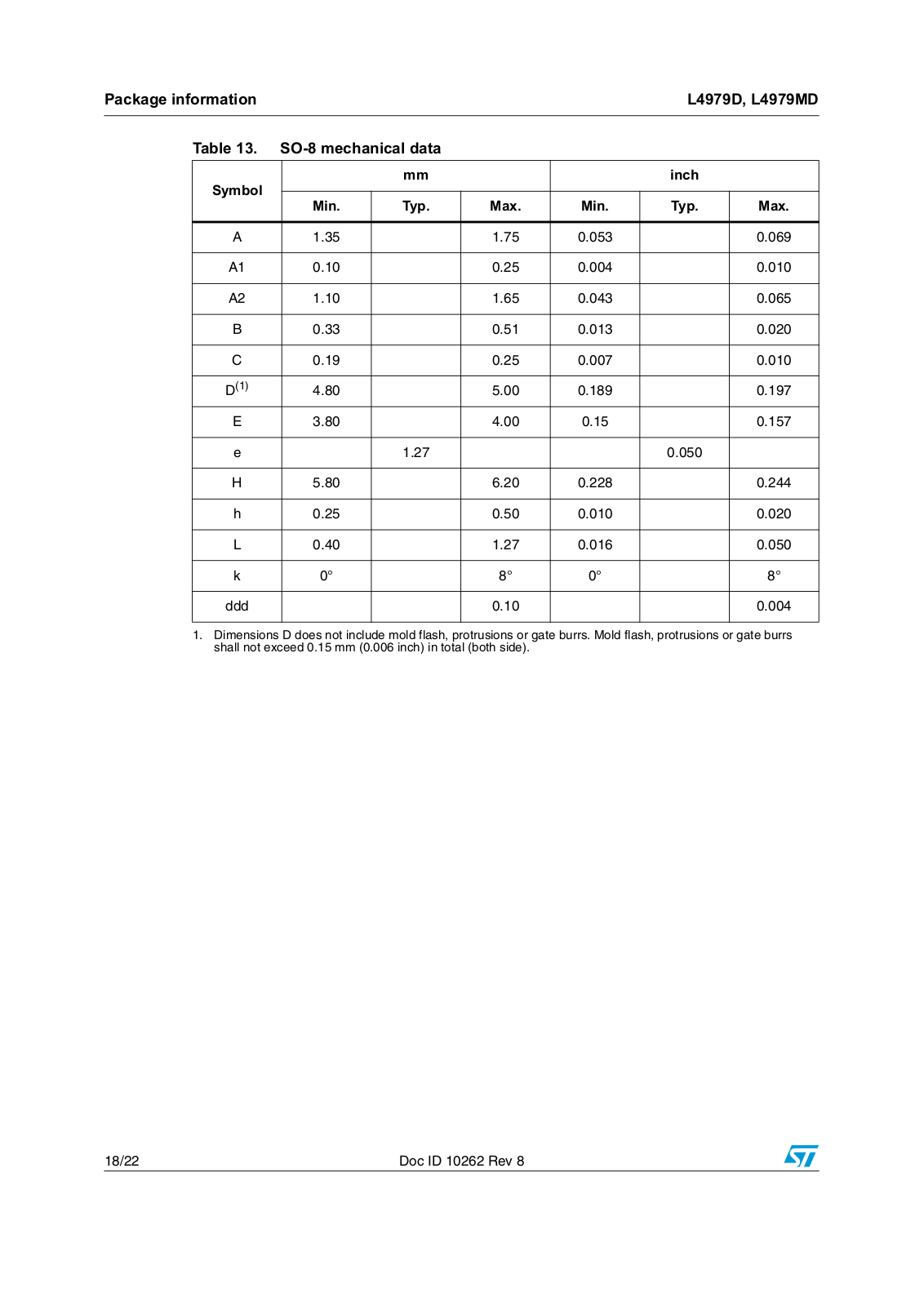
Table of contents
Loading...
ST L4979D, L4979MD User Manual
...
ST User Manual
Download
Specifications and Main Features
Frequently Asked Questions
User Manual
Download
Loading...
+
hidden pages
Unhide
You need points to download manuals.
1 point = 1 manual.
You can buy points or you can get point for every manual you upload.
Buy points
Upload your manuals
 Loading...