

L4971
Fi
1.5A STEP DOWN SWITCHING REGULATOR
1 FEATURES
■ UP TO 1.5A STEP DOWN CONVERTER
■ OPERATING INPUT VOLTAGE FROM 8V TO
55V
■ PRECISE 3.3V (±1%) INTERNAL
REFERENCE VOLTAGE
■ OUTPUT VOLTAGE ADJUSTABLE FROM
3.3V TO 50V
■ SWITCHING FREQUENCY ADJUSTABLE UP
TO 300KHz
■ VOLTAGE FEEDFORWARD
■ ZERO LOAD CURRENT OPERATION
■ INTERNAL CURRENT LIMITING (PULSE-
BYPULSE AND HICCUP MODE)
■ INHIBIT FOR ZERO CURRENT
CONSUMPTION
■ PROTECTION AGAINST FEEDBACK
DISCONNECTION
■ THERMAL SHUTDOWN
■ SOFT START FUNCTION
2 DESCRIPTION
The L4971 is a step down monolithic power
switching regulator delivering 1.5A at a voltage between 3.3V and 50V (selected by a simple external
divider). Realized in BCD mixed technology, the
device uses an internal power D-MOS transistor
(with a typical Rdson of 0.25Ω) to obtain very high
efficency and high switching speed.
gure 1. Package
DIP8
SO16W
Table 1. Order Codes
Part Number Package
L4971 DIP8
L4971D SO16W
L4971D013TR SO16 in Tape & Reel
A switching frequency up to 300KHz is achievable
(the maximum power dissipation of the packages
must be observed).
A wide input voltage range between 8V to 55V and
output voltages regulated from 3.3V to 50V cover
the majority of today’s applications.
Features of this new generations of DC-DC converter include pulse-by-pulse current limit, hiccup
mode for short circuit protection, voltage feedforward regulation, soft-start, protection against feedback loop disconnection, inhibit for zero current
consumption and thermal shutdown.
The device is available in plastic dual in line, DIP8
for standard assembly, and SO16W for SMD assembly.
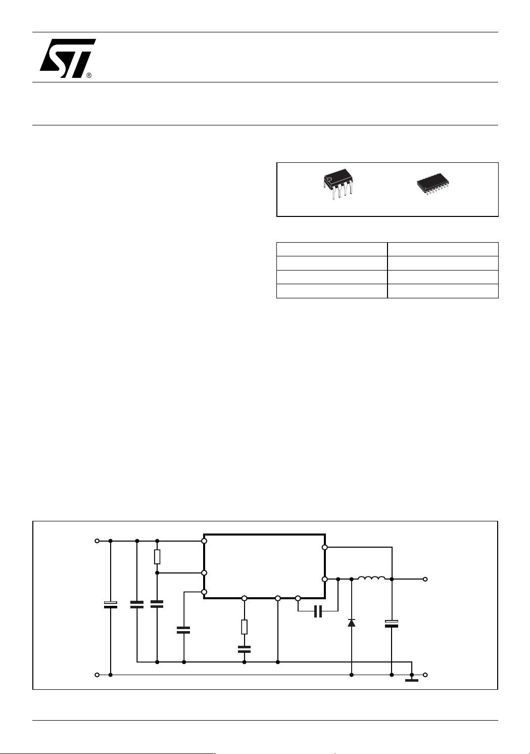
Figure 1. Block Diagram
Vi=8V to 55V
C
220µF
63V
May 2005
C
1
7
220nF
R
1
20K
C
2
2.7nF
C
5
100nF
5
3
2
L4971
7
R
9.1K
22nF
1
2
C
4
6
C
6
100nF
8
4
STPS
3L60U
D97IN748A
D1
L1
126µH
(77120)
C
330µF
VO=3.3V/1.5A
8
Rev. 11
1/13
L4971
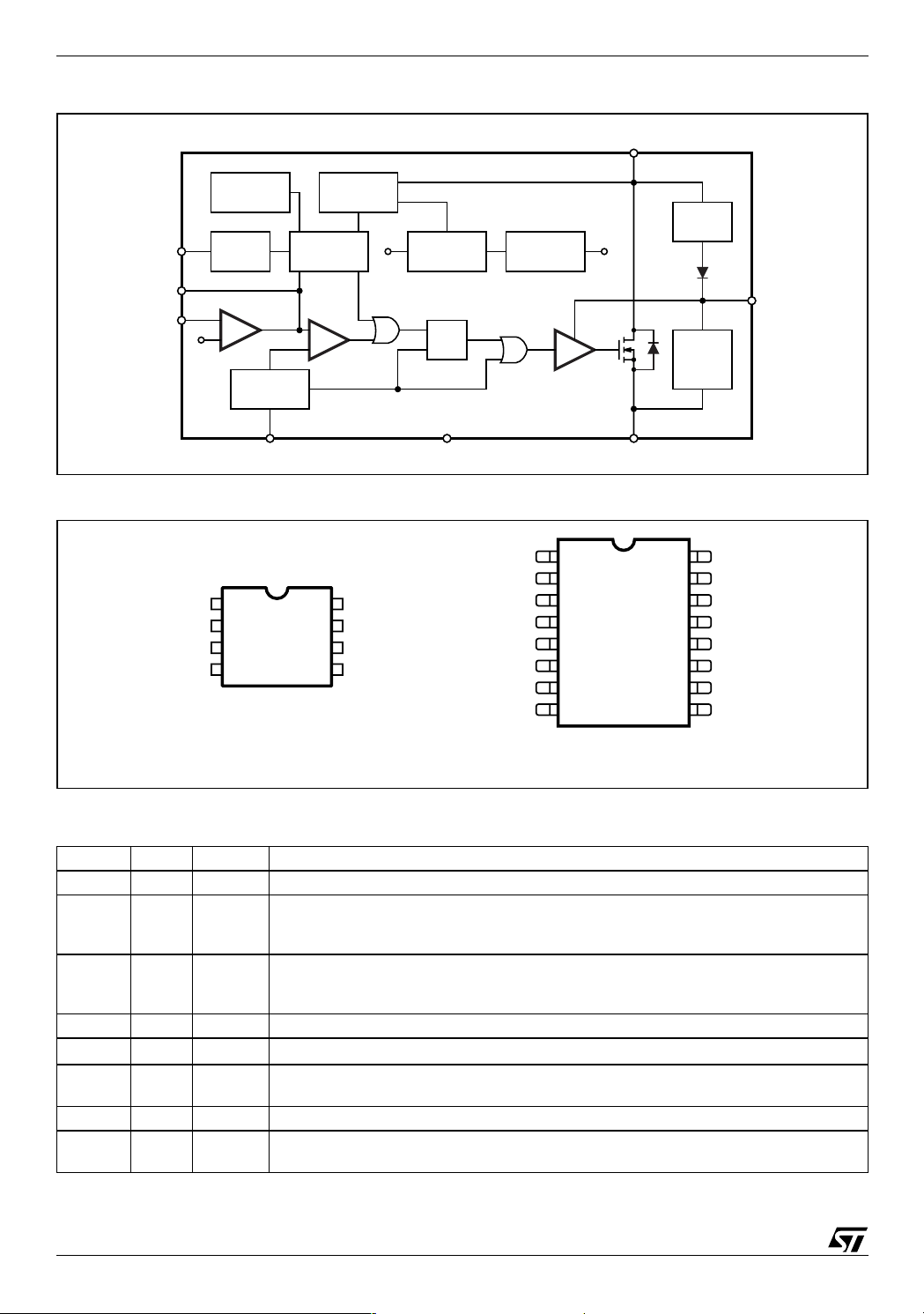
Figure 2. Block Diagram
THERMAL
SHUTDOWN
FB
2
INHIBIT SOFTSTART
7
8
E/A
3.3V
OSCILLATOR
SS_INH
COMP
VOLTAGES
MONITOR
PWM
3.3V
INTERNAL
REFERENCE
R
Q
S
INTERNAL
SUPPLY
5.1V
DRIVE
VCC
5
CBOOT
CHARGE
CBOOT
CHARGE
AT LIGHT
LOADS
6
BOOT
3
OSC GND OUT
1
4
D97IN594
Figure 3. Pin Connections
GND
SS_INH
OSC
OUT
1
2
3
4 VCC
D97IN595
FB8
COMP
7
BOOT
6
5
DIP8
N.C.
GND
SS_INH
OSC
OUT
OUT
N.C.
N.C. N.C.
2
3
4
5
6
7
8
D97IN596
16
15
14
13
12
11
10
SO16
N.C.1
N.C.
FB
COMP
BOOT
VCC
N.C.
9
Table 2. Pin Description
DIP SO (*) Name Function
1 2 GND Ground
2 3 SS_INH A logic signal (active low) disables the device (sleep mode operation).
A capacitor connected between this pin and ground determines the soft start time.
When this pin is grounded disabled the device (driven by open collector/drain).
3 4 OSC An external resistor connected between the unregulated input voltage and this pin and
4 5, 6 OUT Stepdown regulator output
511
VCC
6 12 BOOT A capacitor connected between this pin and OUT allows to drive the internal DMOS
7 13 COMP E/A output to be used for frequency compensation
8 14 FB Stepdown feedback input. Connecting directly to this pin results in an output voltage of
(*) Pins 1, 7, 8, 9, 10, 15 and 16 are not internally, electrically connected to the die.
a capacitor connected from this pin to ground fix the switching frequency. (Line feed
forward is automatically obtained)
Unregulated DC input voltage
Transistor
3.3V. An external resistive divider is required for higher output voltages.
2/13
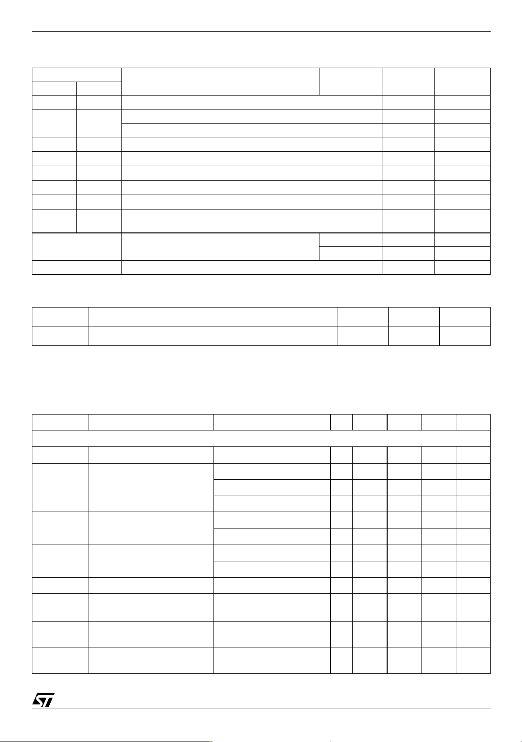
Table 3. Absolute Maximum Ratings
L4971
Symbol
Minidip S016
V
5
V4 V
V
11
5,V6
Input voltage 58 V
Output DC voltage -1 V
Parameter Value Unit
Output peak voltage at t = 0.1µs f=200KHz -5 V
V
I
4
6-V5
V
6
V
7
V
2
V
8
I5,I
V12-V
V
12
V
13
V
V
14
Maximum output current int. limit.
6
11
14 V
Bootstrap voltage 70 V
Analogs input voltage (VCC = 24V 12 V
Analogs input voltage (V
3
= 24V) 13 V
CC
(VCC = 20V) 6
-0.3
P
tot
Power dissipation a Tamb ≤60°C DIP8 1W
SO16 0.8 W
T
j,Tstg
Junction and storage temperature -40 to 150 °C
Table 4. Thermal Data
Symbol Parameter DIP8 SO16 Unit
R
th(j-amb)
(*) Package mounted on board.
Thermal Resistance Junction to ambient Max. 90 (*) 110 (*) °C/W
V
V
3 ELECTRICAL CHARACTERISTCS
Table 5. (Tj = 25°C, Cosc = 2.7nF, Rosc = 20kΩ, VCC = 24V, unless otherwise specified.)
* Specification Refered to T
Symbol Parameter Test Condition Min. Typ. Max. Unit
DYNAMIC CHARACTERISTIC
V
Vo Output voltage Io = 0.5A 3.33 3.36 3.39 V
Vd Dropout voltage Vcc = 10V; Io = 1.5A 0.44 0.55 V
I
l
fs Switching frequency * 90 100 110 KHz
SVRR Supply voltage ripple rejection Vi = Vcc+2V
Operating input voltage range Vo = 3.3 to 50V; Io = 1.5A * 8 55 V
I
Maximum limiting current
Efficiency
Voltage stability of switching
frequency
Temp. stability of switching
frequency
from 0 to 125°C
j
Io = 0.2 to 1.5A 3.292 3.36 3.427 V
Vcc = 8 to 55V * 3.22 3.36 3.5 V
Vcc = 8 to 55V * 2 2.5 3 A
Vo = 3.3V; Io = 1.5A 85 %
Io = 1.5A; f
Vcc = 8 to 55V 3 6 %
Tj = 0 to 125°C 4 %
RMS
ripple
= 100Hz
; Vo = Vref;
*0.88V
60 dB
3/13
L4971
Table 5. (Tj = 25°C, Cosc = 2.7nF, Rosc = 20kΩ, VCC = 24V, unless otherwise specified.)
* Specification Refered to T
Soft Start
Soft start charge current 30 40 50 µA
Soft start discharge current 6 10 14 µA
Inhibit
V
LL
I
sLL
DC Characteristics
Iqop
Iq
Iqst-by
Error Amplifier
V
FB
R
L
V
oH
V
oL
Io source
Io sink
I
b
SVRR E/A Supply voltage ripple rejection V
gm Transconductance I
Oscillator Section
Low level voltage * 0.9 V
Isource Low level * 5 15 µA
Total operating quiescent
current
Quiescent current Duty Cycle = 0; VFB = 3.8V 2.5 3.5 mA
Total stand-by quiescent
current
Voltage Feedback Input 3.33 3.36 3.39 V
Line regulation Vcc = 8 to 55V 5 10 mV
Ref. voltage stability vs
temperature
High level output voltage VFB = 2.5V 10.3 V
Low level output voltage VFB = 3.8V 0.65 V
Source output current V
Sink output current V
Source bias current 2 3 µA
DC open loop gain
Ramp Valley 0.78 0.85 0.92 V
Ramp peak Vcc = 8V 2 2.15 2.3 V
Maximum duty cycle 95 97 %
Maximum Frequency Duty Cycle = 0% ;
from 0 to 125°C
j
V
inh
Vcc = 55V; Vinh<0.9V 150 300 µA
comp
comp
comp
R
= ∞
L
comp
V
comp
Vcc = 55V 9 9.6 10.2 V
R
osc
46mA
<0.9V 100 200 µA
* 0.4 mV/°C
= 6V; VFB = 2.5V 200 300 µA
= 6V; VFB= 3.8V 200 300 µA
= Vfb; Vcc = 8 to 55V 60 80 dB
50 57 dB
= -0.1 to 0.1mA
2.5 ms
= 6V
300 kHz
= 13kΩ, C
= 820pF
osc
4/13
 Loading...