


®
2.5A POWER SWITCHING REGULATOR
2.5A OUTPUT CURRENT
5.1V TO 40V OPUTPUT VOLTAGE RANGE
PRECISE (± 2%) ON-CHIP REFERENCE
HIGH SWITCHING FREQUENCY
VERY HIGH EFFICIENCY (UP TO 90%)
VERY FEW EXTERNAL COMPONENTS
SOFT START
INTERNAL LIMITING CURRENT
THERMAL SHUTDOWN
L4960
HEPTAWATT
ORDERING NUMBERS
L4960H (Horizontal)
: L4960 (Vertical)
DESCRIPTION
The L4960 is a monolithic power switching regulator delivering 2.5A at a voltage variable from 5V to
40V in step down configuration.
Features of the device include current limiting, soft
start, thermal protection and 0 to 100% duty cycle
for continuous operation mode.
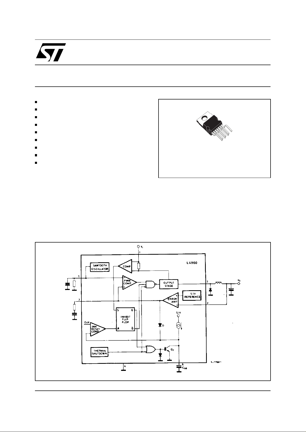
BLOCK DIAGRAM
The L4960 is mounted in a Heptawatt plastic power
package and requires very few external components.
Efficient operation at switching frequencies up to
150KHz allows a reduction in the size and cost of
external filter components.
June 2000
1/16
L4960
PIN CONNECTION
(Top view)
ABSOLUTE MAXIMUM RATINGS
Symbol Parameter Value Unit
V
V
- V7Input to output voltage difference 50 V
1
V
V
3
V
P
T
, T
j
Input voltage 50 V
1
Negative output DC voltage -1 V
7
Negative output peak voltage at t = 0.1µs; f = 100KHz -5 V
, V6Voltage at pin 3 and 6 5.5 V
Voltage at pin 2 7V
2
I
Pin 3 sink current 1 mA
3
I
Pin 5 source current 20 mA
5
Power dissipation at T
tot
Junction and storage temperature -40 to 150
stg
≤ 90°C15W
case
C
°
PIN FUNCTIONS
N
°
NAME
1 SUPPLY VOLTAGE Unregulated voltage input. An internal regulator powers the
internal logic.
2 FEEDBACK INPUT The feedback terminal of the regulation loop. The output is
connected directly to this terminal for 5.1V operation; it is
connected via a divider for higher voltages.
3 FREQUENCY
COMPENSATION
A series RC network connected between this terminal and
ground determines the regulation loop gain characteristics.
4 GROUND Common ground terminal.
5 OSCILLA TOR A parall el RC network connected t o this terminal determines th e
switching frequency.
6 SOFT START Soft start time constant. A capacitor is connected between this
terminal and ground to define the soft start time constant. This
capacitor also determines the average short circuit output
current.
7 OUTPUT Regulator output.
FUNCTION
2/16
THERMAL DATA
Symbol Parameter Value Unit
R
th j-case
R
th j-amb
Thermal resistance junction-case max 4
Thermal resistance junction-ambient max 50
L4960
C/W
°
C/W
°
ELECTRICAL CHARACTERISTICS
(Refer to the test circuit, T
= 25 °C, Vi = 35V, unless otherwise
j
specified)
Symbol Parameter Test Conditions Min. Typ. Max. Unit
DYNAMIC CHARACTERISTICS
V
Output voltage range Vi = 46V Io = 1A V
o
Input voltage range Vo = V
V
i
Line regulation Vi = 10V to 40V Vo = V
V
∆
o
Load regulation Vo = V
V
∆
o
V
Internal reference voltage
ref
Vi = 9V to 46V Io = 1A 5 5.1 5.2 V
to 36V Io = 2.5A 9 46 V
ref
Io = 1A 15 50 mV
ref
ref
Io = 0.5A to 2A 10 30 mV
ref
(pin 2)
V
∆
ref
Average temperature
coefficient of refer voltage
T
∆
V
I
Dropout voltage Io = 2A 1.4 3 V
d
Maximum operating load
om
current
I
Current limiting threshold
7L
(pin 7)
Tj = 0°C to 125°C
= 1A
I
o
Vi = 9V to 46V
V
= V
to 36V
o
ref
Vi = 9V to 46V
= V
V
to 36V
o
ref
2.5 A
3
40 V
0.4
mV/°C
4.5 A
I
I
SVR Supply voltage ripple
Input average current Vi = 46V; output short-circuit 30 60 mA
SH
Efficiency f = 100KHz V
η
= 2A Vo = 12V 85 %
o
= 2V
V
∆
i
rejection
fripple
V
o
= V
= 100Hz
ref
rms
= V
o
Io = 1A
ref
75 %
50 56
f Switching frequency 85 100 115 KHz
f
∆
∆
∆
∆
f
max
T
Voltage stability of
switching frequency
V
i
f
Temperature stability of
switching frequency
T
j
Maximum operating
switching frequency
Thermal shutdown
sd
junction temperature
Vi = 9V to 46V
Tj = 0°C to 125°C
Vo = V
ref
Io = 2A 120 150
0.5
1
150
dB
%
%
KHz
C
°
3/16
L4960
ELECTRICAL CHARACTERISTICS
(continued)
Symbol Parameter Test Conditions Min. Typ. Max. Unit
DC CHARACTERISTICS
I
Quiescent drain current 100% duty cycle
1Q
pins 5 and 7 open
V
= 46V
i
0% duty cycle 15 20 mA
-I
Output leakage current 0% duty cycle 1 mA
7L
30 40 mA
SOFT START
I
6SO
I
Source current 100 140 180
Sink current 50 70 120
6SI
ERROR AMPLIFIER
V
V
I
High level output voltage V2 = 4.7V I3 = 100µA 3.5 V
3H
Low level output voltage V2 = 5.3V I3 = 100µA 0.5V
3L
Sink output current V2 = 5.3V 100 150
3SI
A
µ
A
µ
A
µ
3SO
I
2
Source output current V2 = 4.7V 100 150
Input bias current V2 = 5.2V 2 10
DC open loop gain V3 = 1V to 3V 46 55 dB
v
-I
G
OSCILLATOR
-I
Oscillator source current 5 mA
5
A
µ
A
µ
4/16
L4960
CIRCUIT OPERA TION
(refer to the block diagram)
The L4960 is a monolithic stepdown switching regulator providing output voltages from 5.1V to 40V and
delivering 2.5A.
The regulation loop consists of a sawtooth oscillator, error amplifier, comparator and the output
stage. An error signal is produced by comparing the
output voltage with a precise 5.1V on-chip r eference (zener zap trimmed to ± 2%).
This error signal is then compared with the sawtooth
signal to generate the fixed frequency pulse width
modulated pulses which drive the output stage.
The gain and frequency stability of the loop can be
adjusted by an external RC network connected to
pin 3. Closing the loop directly gives an output
voltage of 5.1V. Higher voltages are obtained by
inserting a voltage divider.
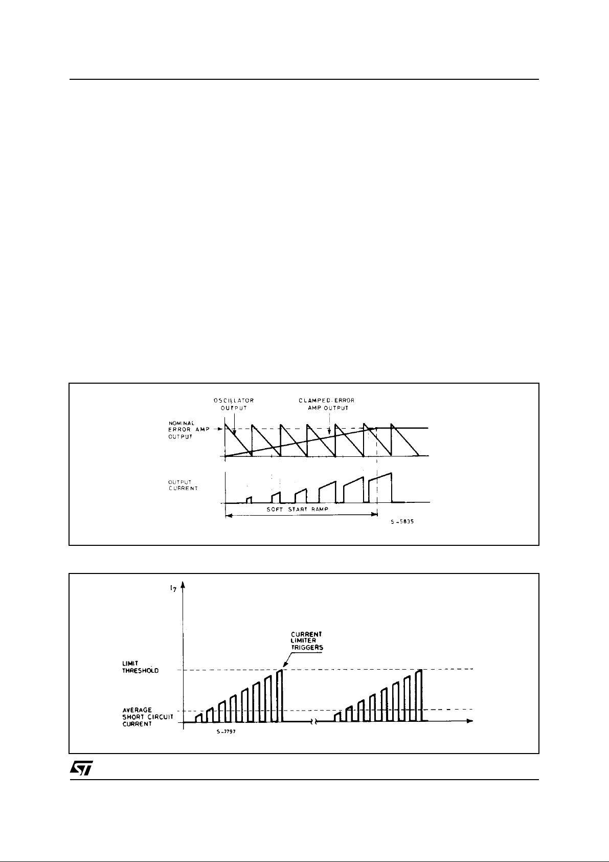
Output overcurrents at switch on are prevented by
the soft start function. The error amplifier output is
initially clamped by the ex ternal capacitor C
ss
and
Figure 1. Soft start waveforms
allowed to rise, linearly, as this capacitor is charged
by a constant current source. Output overload protection is provided in the form of a current limiter.
The load current is sensed by an internal metal
resistor connected to a comparator. When the load
current exceeds a preset threshold this comparator
sets a flip flop which disables the output stage and
discharges the soft start capacitor. A second comparator resets the flip flop when the voltage across
the soft start capacitor has fallen to 0.4V.
The output stage is thus re-enabled and the out put
voltage rises under control of the soft start network.
If the overload condition is still present the limiter
will trigger again when the threshold current is
reached. The average short circuit current is lim ited
to a safe value by the dead time introduced by the
soft start network. The thermal overload circuit disables circuit operation when the junction temperature reaches about 150°C and has hysteresis to
prevent unstable conditions.
Figure 2. Current limiter waveforms
5/16