

Very low drop voltage regulators with inhibit
Features
■ Very low dropout voltage (0.4 V)
■ Very low quiescent current
■ (Typ. 50 µA in off mode, 600 µA in on mode)
■ Output current up to 250 mA
■ Logic-controlled electronic shutdown
■ Output voltages of 2.7; 3.3; 3.5; 5; 8; 12 V
■ Automotive Grade product: 2.7 V, 3.3 V, 3.5 V
V
only in SO-8 package
OUT
■ Internal current and thermal limit
■ Only 2.2 µF for stability
■ Available in ± 1 % (AB) or 2 % (C) selection at
25 °C
■ Supply voltage rejection: 70 dB typ. for 5 V
version
■ Temperature range: -40 to 125 °C
Description
L4931ABxx
L4931Cxx
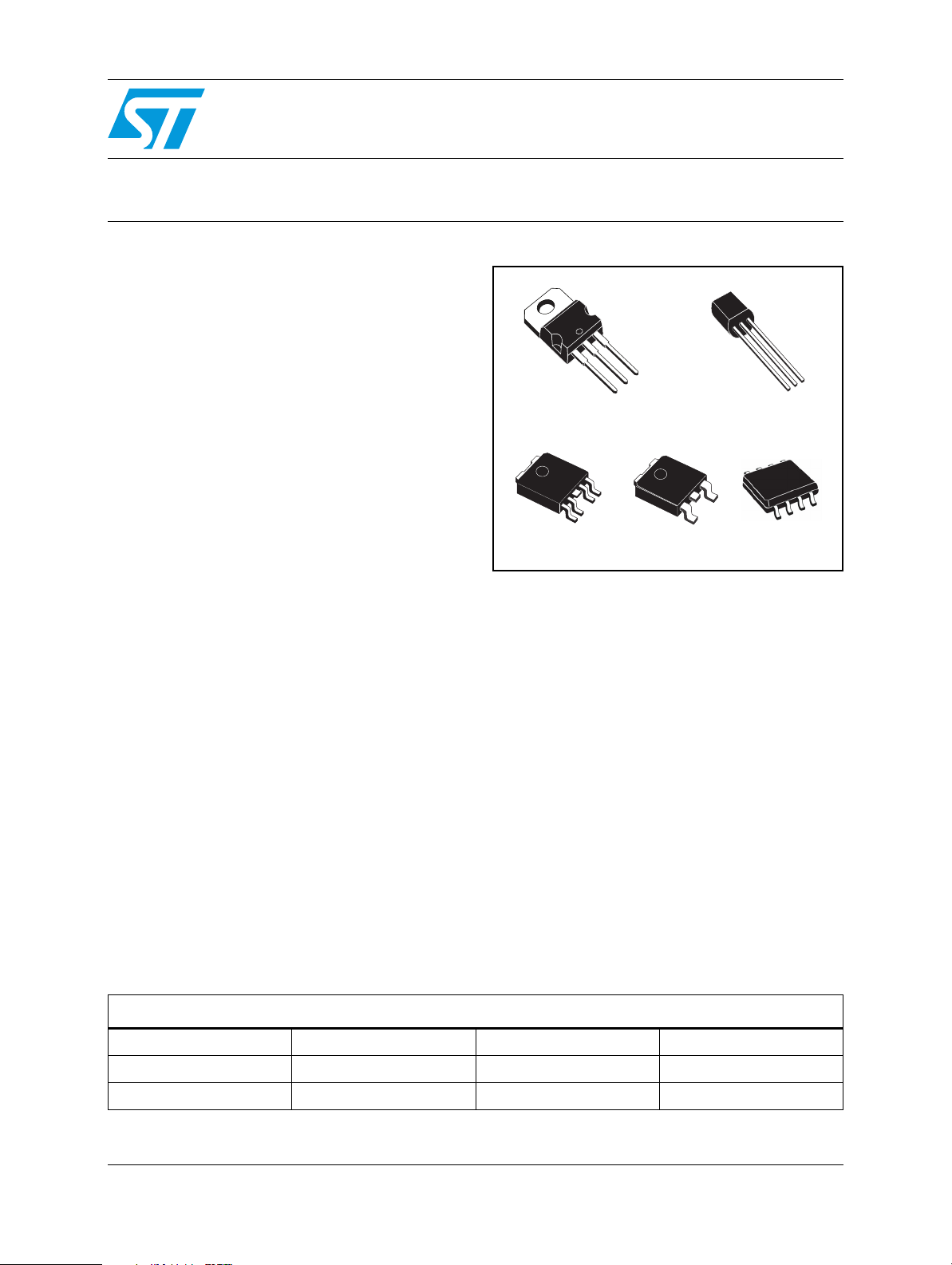
TO-220
PPAK SO-8
DPAK
This means that when the device is used as a
local regulator, it is possible to put a part of the
board in standby, decreasing the total power
consumption. It requires only a 2.2 µF capacitor
for stability allowing space and cost saving.
TO-92
The L4931ABxx L4931Cxx are very Low Drop
regulators available in TO-220, SO-8, DPAK,
PPAK and TO-92 packages and in a wide range of
output voltages.
The L4931 is available as Automotive Grade in
SO-8 package only, for the options of output
voltages whose commercial Part Numbers are
shown in the Table 19 on page 34 (order codes).
These devices are qualified according to the
The very low drop voltage (0.4 V) and the very low
quiescent current make them particularly suitable
for low noise, low power applications and
specially in battery powered systems.
specification AEC-Q100 of the Automotive
market, in the temperature range -40 °C to
125 °C, and the statistical tests PAT, SYL, SBL are
performed.
A TTL compatible shutdown logic control function
is available in PPAK and SO-8 packages.
Table 1. Device summary
Part numbers
L4931ABXX27 L4931CXX33 L4931ABXX50 L4931CXX80
L4931CXX27 L4931ABXX35 L4931CXX50 L4931ABXX120
L4931ABXX33 L4931CXX35 L4931ABXX80 L4931CXX120
August 2008 Rev 17 1/36
www.st.com
36

Contents L4931ABxx - L4931Cxx
Contents
1 Diagram . . . . . . . . . . . . . . . . . . . . . . . . . . . . . . . . . . . . . . . . . . . . . . . . . . . 5
2 Pin configuration . . . . . . . . . . . . . . . . . . . . . . . . . . . . . . . . . . . . . . . . . . . 6
3 Maximum ratings . . . . . . . . . . . . . . . . . . . . . . . . . . . . . . . . . . . . . . . . . . . . 7
4 Application circuit . . . . . . . . . . . . . . . . . . . . . . . . . . . . . . . . . . . . . . . . . . 8
5 Electrical characteristics . . . . . . . . . . . . . . . . . . . . . . . . . . . . . . . . . . . . . 9
6 Typical application . . . . . . . . . . . . . . . . . . . . . . . . . . . . . . . . . . . . . . . . . 24
7 Package mechanical data . . . . . . . . . . . . . . . . . . . . . . . . . . . . . . . . . . . . 25
8 Order codes . . . . . . . . . . . . . . . . . . . . . . . . . . . . . . . . . . . . . . . . . . . . . . 34
9 Revision history . . . . . . . . . . . . . . . . . . . . . . . . . . . . . . . . . . . . . . . . . . . 35
2/36

L4931ABxx - L4931Cxx List of figures
List of figures
Figure 1. Schematic diagram . . . . . . . . . . . . . . . . . . . . . . . . . . . . . . . . . . . . . . . . . . . . . . . . . . . . . . . . 5
Figure 2. Pin connections (top view) . . . . . . . . . . . . . . . . . . . . . . . . . . . . . . . . . . . . . . . . . . . . . . . . . . 6
Figure 3. Test circuit . . . . . . . . . . . . . . . . . . . . . . . . . . . . . . . . . . . . . . . . . . . . . . . . . . . . . . . . . . . . . . 8
Figure 4. Line regulation vs temperature . . . . . . . . . . . . . . . . . . . . . . . . . . . . . . . . . . . . . . . . . . . . . . 24
Figure 5. Dropout voltage vs temperature . . . . . . . . . . . . . . . . . . . . . . . . . . . . . . . . . . . . . . . . . . . . . 24
Figure 6. Supply current vs input voltage. . . . . . . . . . . . . . . . . . . . . . . . . . . . . . . . . . . . . . . . . . . . . . 24
Figure 7. Supply current vs temperature . . . . . . . . . . . . . . . . . . . . . . . . . . . . . . . . . . . . . . . . . . . . . . 24
Figure 8. Short circuit current vs dropout voltage . . . . . . . . . . . . . . . . . . . . . . . . . . . . . . . . . . . . . . . 24
Figure 9. SVR vs input voltage signal frequency . . . . . . . . . . . . . . . . . . . . . . . . . . . . . . . . . . . . . . . . 24
3/36

List of tables L4931ABxx - L4931Cxx
List of tables
Table 1. Device summary . . . . . . . . . . . . . . . . . . . . . . . . . . . . . . . . . . . . . . . . . . . . . . . . . . . . . . . . . . 1
Table 2. Absolute maximum ratings . . . . . . . . . . . . . . . . . . . . . . . . . . . . . . . . . . . . . . . . . . . . . . . . . . 7
Table 3. Thermal data. . . . . . . . . . . . . . . . . . . . . . . . . . . . . . . . . . . . . . . . . . . . . . . . . . . . . . . . . . . . . 7
Table 4. Electrical characteristics of L4931ABxx27 . . . . . . . . . . . . . . . . . . . . . . . . . . . . . . . . . . . . . . 9
Table 5. Electrical characteristics of L4931Cxx27 . . . . . . . . . . . . . . . . . . . . . . . . . . . . . . . . . . . . . . 10
Table 6. Electrical characteristics of L4931Cxx27-TRY (Automotive Grade) . . . . . . . . . . . . . . . . . . 11
Table 7. Electrical characteristics of L4931ABxx33 . . . . . . . . . . . . . . . . . . . . . . . . . . . . . . . . . . . . . 12
Table 8. Electrical characteristics of L4931Cxx33 . . . . . . . . . . . . . . . . . . . . . . . . . . . . . . . . . . . . . . 13
Table 9. Electrical characteristics of L4931Cxx33-TRY (Automotive Grade) . . . . . . . . . . . . . . . . . . 14
Table 10. Electrical characteristics of L4931ABxx35 . . . . . . . . . . . . . . . . . . . . . . . . . . . . . . . . . . . . . 15
Table 11. Electrical characteristics of L4931ABxx35-TRY (Automotive Grade) . . . . . . . . . . . . . . . . . 16
Table 12. Electrical characteristics of L4931Cxx35 . . . . . . . . . . . . . . . . . . . . . . . . . . . . . . . . . . . . . . 17
Table 13. Electrical characteristics of L4931ABxx50 . . . . . . . . . . . . . . . . . . . . . . . . . . . . . . . . . . . . . 18
Table 14. Electrical characteristics of L4931Cxx50 . . . . . . . . . . . . . . . . . . . . . . . . . . . . . . . . . . . . . . 19
Table 15. Electrical characteristics of L4931ABxx80 . . . . . . . . . . . . . . . . . . . . . . . . . . . . . . . . . . . . . 20
Table 16. Electrical characteristics of L4931Cxx80 . . . . . . . . . . . . . . . . . . . . . . . . . . . . . . . . . . . . . . 21
Table 17. Electrical characteristics of L4931ABxx120 . . . . . . . . . . . . . . . . . . . . . . . . . . . . . . . . . . . . 22
Table 18. Electrical characteristics of L4931Cxx120 . . . . . . . . . . . . . . . . . . . . . . . . . . . . . . . . . . . . . 23
Table 19. Order codes . . . . . . . . . . . . . . . . . . . . . . . . . . . . . . . . . . . . . . . . . . . . . . . . . . . . . . . . . . . . 34
Table 20. Document revision history . . . . . . . . . . . . . . . . . . . . . . . . . . . . . . . . . . . . . . . . . . . . . . . . . 35
4/36
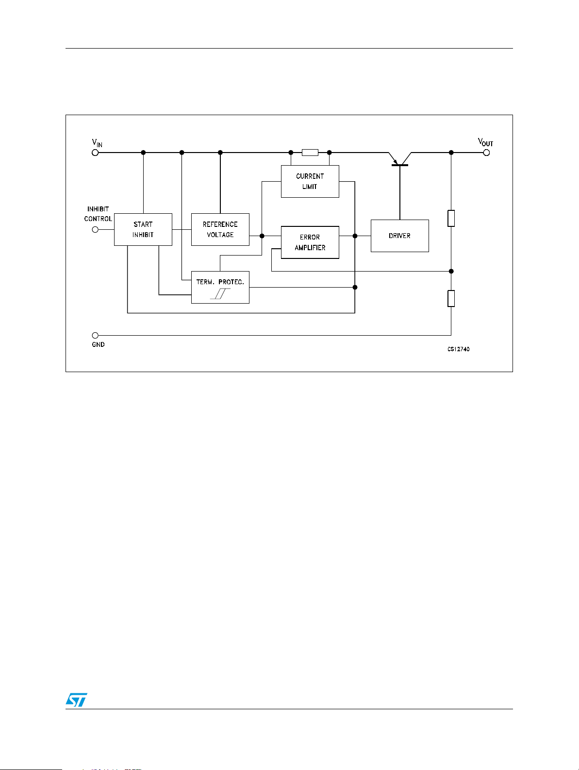
L4931ABxx - L4931Cxx Diagram
1 Diagram
Figure 1. Schematic diagram
5/36
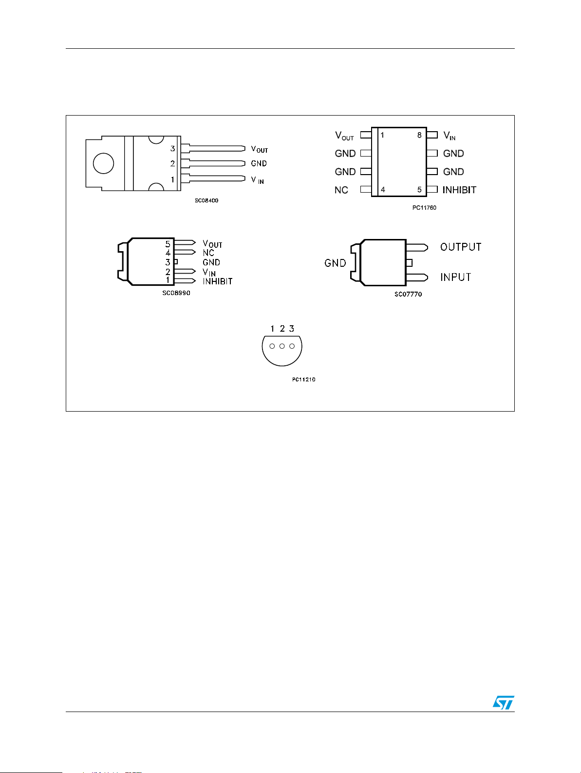
Pin configuration L4931ABxx - L4931Cxx
2 Pin configuration
Figure 2. Pin connections (top view)
TO-220
PPAK
TO-92
PIN 1 = V
OUT
PIN 2 = GND
PIN 3 = V
IN
BOTTOM VIEW
SO-8
DPAK
6/36
L4931ABxx - L4931Cxx Maximum ratings
3 Maximum ratings
Table 2. Absolute maximum ratings
Symbol Parameter Value Unit
T
V
I
P
STG
T
I
O
D
OP
DC Input voltage 20 V
Output current Internally limited mA
Power dissipation Internally limited mW
Storage temperature range -40 to 150 °C
Operating junction temperature range -40 to 125 °C
Note: Absolute maximum ratings are those values beyond which damage to the device may occur.
Functional operation under these condition is not implied
Table 3. Thermal data
Symbol Parameter TO-220 SO-8 DPAK PPAK TO-92 Unit
R
R
Thermal resistance junction-case 3 20 8 8 °C/W
thJC
Thermal resistance junction-ambient 50 55 100 100 200 °C/W
thJA
7/36
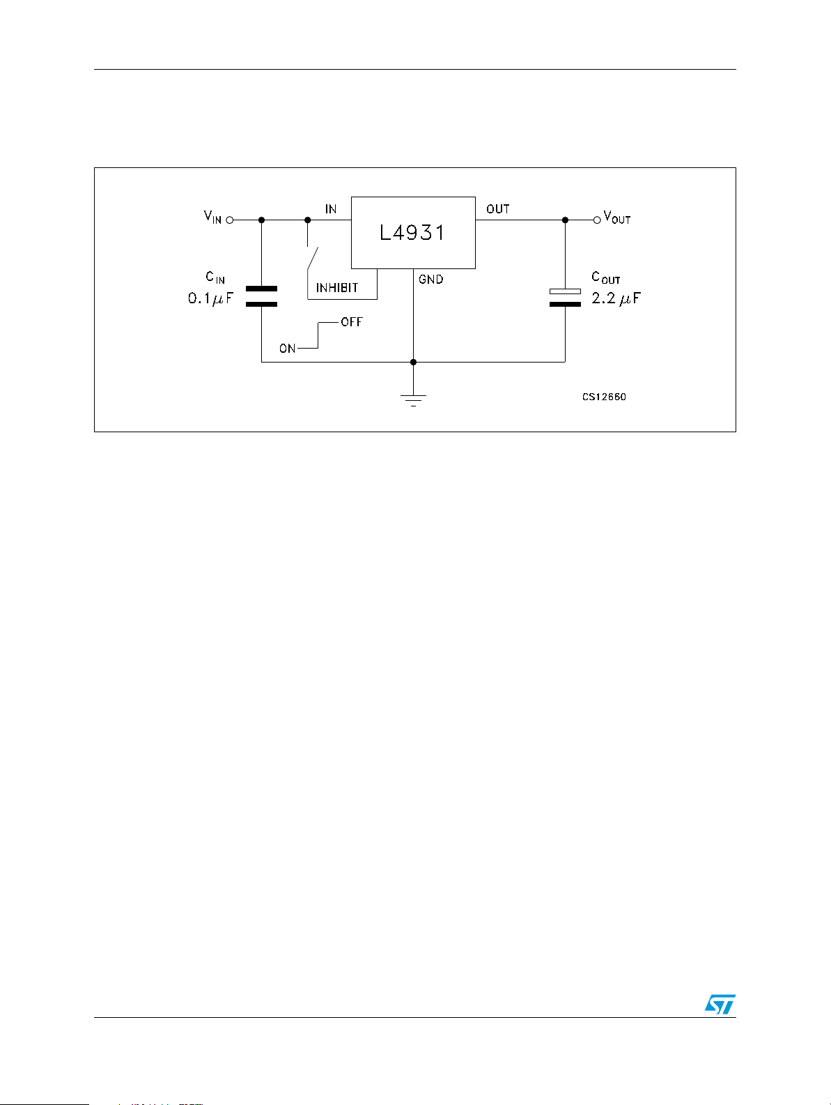
Application circuit L4931ABxx - L4931Cxx
4 Application circuit
Figure 3. Test circuit
8/36
L4931ABxx - L4931Cxx Electrical characteristics
5 Electrical characteristics
Table 4. Electrical characteristics of L4931ABxx27 (refer to the test circuits, TA = 25 °C,
C
= 0.1 µF, CO = 2.2 µF unless otherwise specified).
I
Symbol Parameter Test conditions Min. Typ. Max. Unit
I
= 5 mA, VI = 4.7 V 2.673 2.7 2.727
V
Output voltage
O
V
Operating input voltage IO = 250 mA 20 V
I
Output current limit 300 mA
I
out
ΔV
ΔV
Line regulation VI = 3.4 to 20 V, IO = 0.5 mA 3 15 mV
O
Load regulation
O
(1)
Quiescent current
ON MODE
I
d
OFF MODE V
SVR Supply voltage rejection
eN Output noise voltage B = 10 Hz to 100 kHz 50 µV
V
Dropout voltage
d
Control input logic low TA = -40 to 125°C 0.8 V
V
IL
Control Input Logic High TA = -40 to 125°C 2 V
V
IH
I
Control input current VI = 6 V, VC = 6 V 10 µA
I
Output bypass
C
O
capacitance
(1)
O
= 5 mA, VI = 4.7 V, TA=-25 to 85°C 2.646 2.754
I
O
V
VI = 3.6 V, IO = 0.5 to 250 mA 3 15 mV
= 3.6 to 20 V, IO = 0 mA 0.6 1
V
I
= 3.6 to 20 V, IO = 250 mA 4 6
V
I
= 6 V 50 100 µA
I
mA
f = 120 Hz 74
I
= 5 mA
O
VI = 4.6 ± 1 V
dBf = 1 kHz 71
f = 10 kHz 55
IO = 250 mA 0.4 0.6 V
I
= 250 mA, TA= -40 to 125°C 0.8 V
O
ESR = 0.1 to 10 Ω, I
= 0 to 250 mA 2 10 µF
O
1. For SO-8 package the maximum limit of load regulation and dropout is increased by 20 mV.
9/36
Electrical characteristics L4931ABxx - L4931Cxx
Table 5. Electrical characteristics of L4931Cxx27 (refer to the test circuits, TA = 25 °C,
C
= 0.1 µF, CO = 2.2 µF unless otherwise specified).
I
Symbol Parameter Test conditions Min. Typ. Max. Unit
I
= 5 mA, VI = 4.7 V 2.646 2.7 2.754
V
Output voltage
O
V
Operating input voltage IO = 250 mA 20 V
I
Output current limit 300 mA
I
out
ΔV
ΔV
Line regulation VI = 3.4 to 20 V, IO = 0.5 mA 3 18 mV
O
Load regulation
O
(1)
Quiescent current
ON MODE
I
d
OFF MODE V
SVR Supply voltage rejection
eN Output noise voltage B = 10 Hz to 100 kHz 50 µV
V
Dropout voltage
d
Control input logic low TA = -40 to 125°C 0.8 V
V
IL
Control Input Logic High TA = -40 to 125°C 2 V
V
IH
I
Control input current VI = 6 V, VC = 6 V 10 µA
I
Output bypass
C
O
capacitance
(1)
O
= 5 mA, VI = 4.7 V, TA=-25 to 85°C 2.592 2.808
I
O
V
VI = 3.6 V, IO = 0.5 to 250 mA 3 18 mV
= 3.6 to 20 V, IO = 0 mA 0.6 1
V
I
= 3.6 to 20 V, IO = 250 mA 4 6
V
I
= 6 V 50 100 µA
I
mA
f = 120 Hz 74
I
= 5 mA
O
VI = 4.6 ± 1 V
dBf = 1 kHz 71
f = 10 kHz 55
IO = 250 mA 0.4 0.6 V
I
= 250 mA, TA= -40 to 125°C 0.8 V
O
ESR = 0.1 to 10 Ω, I
= 0 to 250 mA 2 10 µF
O
1. For SO-8 package the maximum limit of load regulation and dropout is increased by 20 mV.
10/36
L4931ABxx - L4931Cxx Electrical characteristics
Table 6. Electrical characteristics of L4931Cxx27-TRY (Automotive Grade) (refer to the test
circuits, T
Symbol Parameter Test conditions Min. Typ. Max. Unit
V
Output voltage
O
V
Operating input voltage IO = 250 mA 20 V
I
Output current limit TA = 25°C 300 mA
I
out
ΔV
ΔV
SVR Supply voltage rejection
Line regulation VI = 3.4 to 20 V, IO = 0.5 mA 20 mV
O
Load regulation VI = 3.6 V, IO = 0.5 to 250 mA 38 mV
O
Quiescent current
ON MODE
I
d
OFF MODE V
eN Output noise voltage B = 10 Hz to 100 kHz, T
V
Dropout voltage
d
Control input logic low 0.82 V
V
IL
Control Input Logic High 2 V
V
IH
I
Control input current VI = 6 V, VC = 6 V, TA = 25°C 10 µA
I
Output bypass
C
O
capacitance
= -40 to 12 5°C, CI = 0.1 µF, CO = 2.2 µF unless otherwise specified).
A
I
= 5 mA, VI = 4.7 V, TA = 25°C 2.646 2.7 2.754
O
= 5 mA, VI = 4.7 V 2.592 2.808
I
O
= 3.6 to 20 V, IO = 0 mA 1
V
I
= 3.6 to 20 V, IO = 250 mA 6
V
I
= 6 V 100 µA
I
I
= 5 mA
O
f = 120 Hz 74
VI = 4.6 ± 1 V
= 25°C
T
A
I
= 250 mA, TA = 25°C 0.4 0.6 V
O
I
= 250 mA 0.82 V
O
ESR = 0.1 to 10 Ω, IO = 0 to 250 mA,
TA = 25°C
f = 10 kHz 55
= 25°C 50 µV
A
210 µF
V
mA
dBf = 1 kHz 71
11/36
 Loading...