

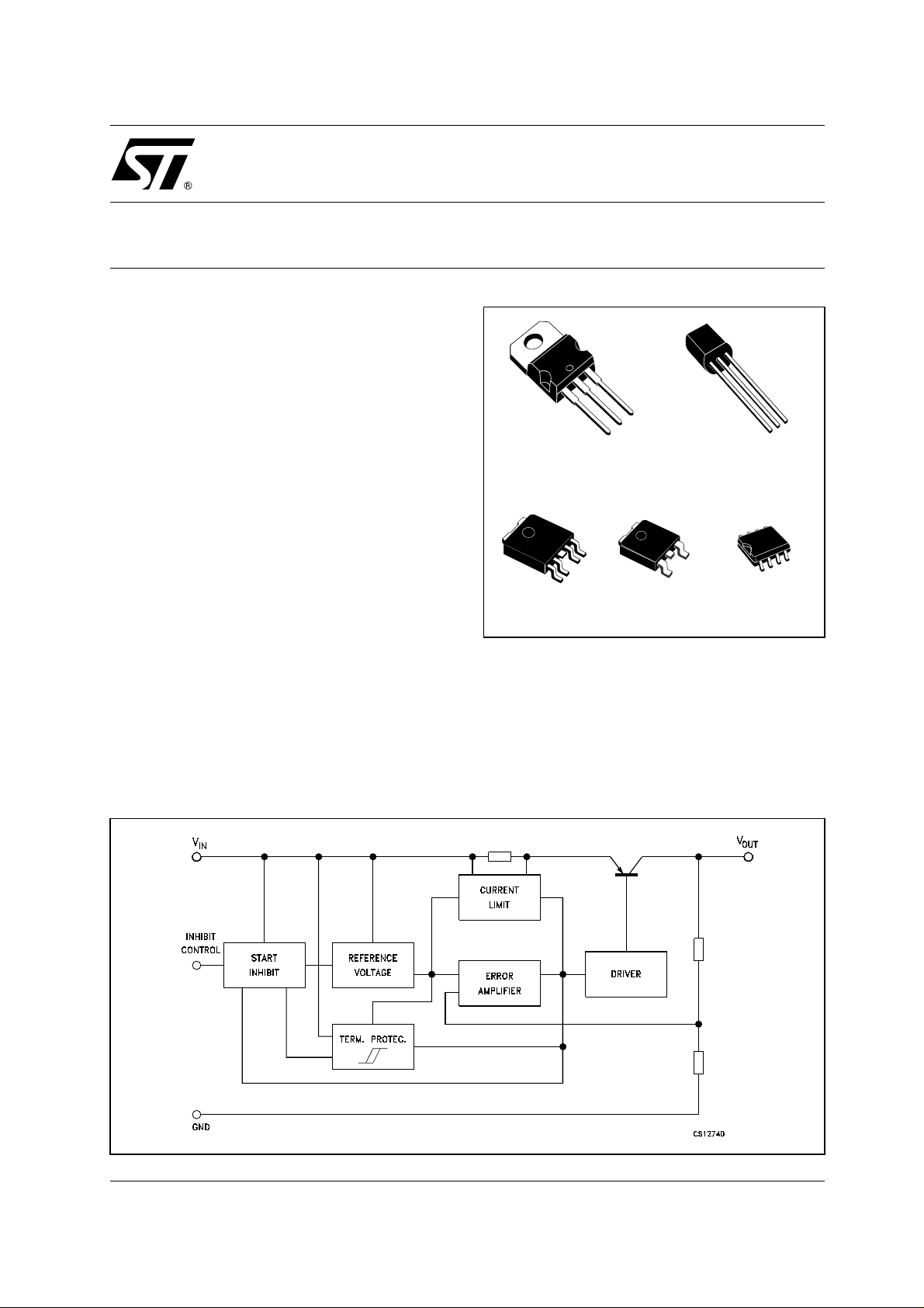
VOLTAGE REGULATORS WITH INHIBIT
■ VERY LOW DROPOUT VOLTAGE (0.4V)
■ VERY LOW QUIESCENT CURRENT
(TYP. 50 µA IN OFF MODE, 600µA IN ON
MODE)
■ OUTPUT CURRENT UP TO 250 mA
■ LOGIC-CONTROLLED ELECTRONIC
SHUTDOWN
■ OUTPUT VOLTAGES OF 1.25; 1.5; 2.5; 2.7;
3; 3.3; 3.5; 4; 4.5; 4.7; 5; 5.2; 5.5; 6; 8; 12V
■ INTERNAL CURRE NT AND THERMAL LIMIT
■ ONLY 2.2µF FOR STABILITY
■ AVAILABLE IN ± 1% (AB) OR 2% (C)
SELECTION AT 25°C
■ SUPPLY VOLTAGE R EJE CTION: 70db TYP.
FOR 5V VERSION
■ TEMPERATURE RANGE: -40 TO 125°C
TO-220
L4931
SERIES
VERY LOW DROP
TO-92
DESCRIPTION
The L4931 series are very Low Drop regulators
available in TO-220, SO-8, DPAK, PPAK and
TO-92 packages and in a wide range of output
voltages.
The very Low Drop voltage (0.4V) and the v ery
low quiescent current make them particularly
suitable for Low Noise, Low Power applications
and s pecially in bat tery powered system s .
SCHEMATIC DIAGRAM
DPAKPPAK
SO-8
In P PAK and SO-8 packages a Shut down Logic
Control function is av ailable TTL compatible. This
means that when the device is used as a local
regulator, it is possible to put a part of the board in
standby, decreasing the total power consumption.
It requires only a 2.2 µF capacitor for stability
allowing space and cost saving.
1/29January 2004
L4931 SERIES
ABSOLUTE MAXIMUM RATINGS
Symbol Parameter Value Unit
V
I
P
T
T
Absolute Maximum Ratings are those values beyond which damage to the device may occur. Functional operation under these condition is
not implied.
THERMAL DATA
Symbol Parameter TO-220 SO-8 DPAK PPAK TO-92 Unit
R
thj-case
R
thj-amb
(*) Considering 6 cm2of copper board heat-sink
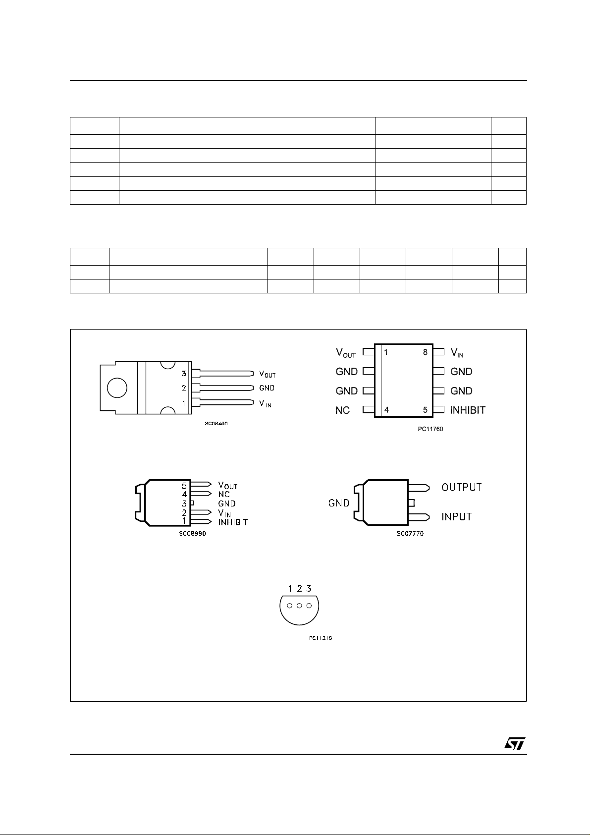
CONNECTION DIAGRAM (top view)
DC Input Voltage
I
Output Current
O
Power Dissipation
tot
Storage Temperature Range
stg
Operating Junction Temperature Range
op
Thermal Resistance Junction-case
Thermal Resistance Junction-ambient
20 V
Internally Limited
Internally Limited
-40 to 150 °C
-40 to 125 °C
3208 8 °C/W
50 55(*) 100 100 200 °C/W
TO-220 SO-8
PPAK
PIN 1 = V
PIN 2 = GND
PIN 3 = V
OUT
IN
DPAK
TO-92
BOTTOM VIEW
2/29
ORDERING CODES
L4931 SERIES
TO-220 SO-8 PPAK DPAK TO-92
L4931CV12 (*) L4931CD12 (*) L4931CPT12 (*) L4931CDT12 (*) L4931CZ12 (*) 1.25 V
L4931ABV12 (*) L4931ABD12 (*) L4931ABPT12 (*) L4931ABDT12 (*) L4931ABZ12 (*) 1.25 V
L4931CV15 (*) L4931CD15 (*) L4931CPT15 (*) L4931CDT15 (*) L4931CZ15 (*) 1.5 V
L4931ABV15 (*) L4931ABD15 (*) L4931ABPT15 (*) L4931ABDT15 (*) L4931ABZ15 (*) 1.5 V
L4931CV25 (*) L4931CD25 L4931CPT25 (*) L4931CDT25 L4931CZ25 (*) 2.5 V
L4931ABV25 (*) L4931ABD25 L4931ABPT25 (*) L4931ABDT25 L4931ABZ25 (*) 2.5 V
L4931CV27 L4931CD27 L4931CPT27 L4931CDT27 L4931CZ27 2.7 V
L4931ABV27 L4931ABD27 L4931ABPT27 L4931ABDT27 L4931ABZ27 2.7 V
L4931CV30 L4931CD30 L4931CPT30 L4931CDT30 L4931CZ30 3 V
L4931ABV30 L4931ABD30 L4931ABPT30 L4931ABDT30 L4931ABZ30 3 V
L4931CV33 L4931CD33 L4931CPT33 L4931CDT33 L4931CZ33 3.3 V
L4931ABV33 L4931ABD33 L4931ABPT33 L4931ABDT33 L4931ABZ33 3.3 V
L4931CV35 L4931CD35 L4931CPT35 L4931CDT35 L4931CZ35 3.5 V
L4931ABV35 L4931ABD35 L4931ABPT35 L4931ABDT35 L4931ABZ35 3.5 V
L4931CV40 L4931CD40 L4931CPT40 L4931CDT40 L4931CZ40 4 V
L4931ABV40 L4931ABD40 L4931ABPT40 L4931ABDT40 L4931ABZ40 4 V
L4931CV45 (*) L4931CD45 (*) L4931CPT45 (*) L4931CDT45 (*) L4931CZ45 (*) 4.5 V
L4931ABV45 (*) L4931ABD45 (*) L4931ABPT45 (*) L4931ABDT45 (*) L4931ABZ45 (*) 4.5 V
L4931CV47 L4931CD47 L4931CPT47 L4931CDT47 L4931CZ47 4.75 V
L4931ABV47 L4931ABD47 L4931ABPT47 L4931ABDT47 L4931ABZ47 4.75 V
L4931CV50 L4931CD50 L4931CPT50 L4931CDT50 L4931CZ50 5 V
L4931ABV50 L4931ABD50 L4931ABPT50 L4931ABDT50 L4931ABZ50 5 V
L4931CV52 (*) L4931CD52 (*) L4931CPT52 (*) L4931CDT52 (*) L4931CZ52 (*) 5.2 V
L4931ABV52 (*) L4931ABD52 (*) L4931ABPT52 (*) L4931ABDT52 (*) L4931ABZ52 (*) 5.2 V
L4931CV55 (*) L4931CD55 (*) L4931CPT55 (*) L4931CDT55 (*) L4931CZ55 (*) 5.5 V
L4931ABV55 (*) L4931ABD55 (*) L4931ABPT55 (*) L4931ABDT55 (*) L4931ABZ55 (*) 5.5 V
L4931CV60 L4931CD60 L4931CPT60 L4931CDT60 L4931CZ60 6 V
L4931ABV60 L4931ABD60 L4931ABPT60 L4931ABDT60 L4931ABZ60 6 V
L4931CV80 L4931CD80 L4931CPT80 L4931CDT80 L4931CZ80 8 V
L4931ABV80 L4931ABD80 L4931ABPT80 L4931ABDT80 L4931ABZ80 8 V
L4931CV120 L4931CD120 L4931CPT120 L4931CDT120 L4931CZ120 12 V
L4931ABV120 L4931ABD120 L4931ABPT120 L4931ABDT120 L4931ABZ120 12 V
OUTPUT
VOLTAGE
(*) Available on request.
3/29
L4931 SERIES
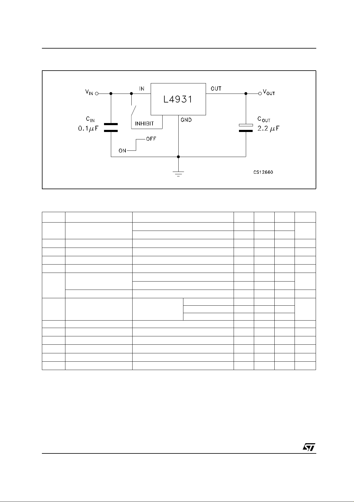
TEST CIRCUITS
ELECTRICAL CHARACTERISTICS OF L4931ABxx12 (refer t o the test circuits, T
=0.1µF,CO= 2.2 µ F unless otherwise spec ified).
C
I
= 25° C,
J
Symbol Parameter Test Conditions Min. Typ. Max. Unit
V
Output Voltage IO=5mA VI= 3.3 V 1.238 1.25 1.263 V
O
=5mA VI=3.3V TA=-25 to 85°C 1.225 1.275
I
O
V
Operating Input Voltage IO= 250 mA 2.5 20 V
I
I
Output Current Limit 300 mA
out
∆V
∆V
SVR Supply Voltage Rejection I
Line Regulation VI= 2.5 to 20 V IO=0.5mA 3 15 mV
O
(*) Load Regulation VI=2.7V IO= 0.5 to 250 mA 3 15 mV
O
Quiescent Current
I
d
ON MODE
OFF MODE V
VI= 2.7 to 20 V IO=0mA 0.61mA
V
= 2.7 to 20 V IO= 250 mA 4 6
I
=6V 50 100 µA
I
=5mA
O
V
=3.7±1V
I
f = 120 Hz 80 dB
f=1KHz 77
f=10KHz 55
eN Output Noise Voltage B =10 Hz to 100 KHz 50 µV
V
(*) Dropout Voltage IO= 250 mA 1.25 V
d
V
Control Input Logic Low TA= -40 to 125°C 0.8 V
IL
Control Input Logic High TA= -40 to 125°C 2 V
V
IH
I
Control Input Current VI=6V, VC=6V 10 µA
I
Output Bypass Capacitance ESR = 0.1 to 10 Ω IO= 0 to 250mA 2 10 µF
C
O
(*) For SO-8 package the maximum limit of load regulation and dropout is increased by 20 mV.
4/29
L4931 SERIES
ELECTRICAL CHARACTERISTICS OF L4931Cxx12 (refer to the test circuits, TJ= 25° C,
=0.1µF,CO= 2.2 µ F unless otherwise spec ified).
C
I
Symbol Parameter Test Conditions Min. Typ. Max. Unit
V
Output Voltage IO=5mA VI= 3.3 V 1.225 1.25 1.275 V
O
I
=5mA VI=3.3V TA=-25 to 85°C 1.2 1.3
O
Operating Input Voltage IO= 250 mA 2.5 20 V
V
I
Output Current Limit 300 mA
I
out
∆V
∆V
SVR Supply Voltage Rejection I
V
(*) For SO-8 package the maximum limit of load regulation and dropout is increased by 20 mV.
Line Regulation VI= 2.5 to 20 V IO=0.5mA 3 18 mV
O
(*) Load Regulation VI=2.7V IO= 0.5 to 250 mA 3 18 mV
O
Quiescent Current
I
d
ON MODE
OFF MODE V
VI= 2.7 to 20 V IO=0mA 0.61mA
= 2.7 to 20 V IO= 250 mA 4 6
V
I
=6V 50 100 µA
I
=5mA
O
V
=3.7±1V
I
f = 120 Hz 80 dB
f=1KHz 77
f=10KHz 55
eN Output Noise Voltage B =10 Hz to 100 KHz 50 µV
(*) Dropout Voltage IO= 250 mA 1.25 V
d
Control Input Logic Low TA= -40 to 125°C 0.8 V
V
IL
V
Control Input Logic High TA= -40 to 125°C 2 V
IH
Control Input Current VI=6V, VC=6V 10 µA
I
I
Output Bypass Capacitance ESR = 0.1 to 10 Ω IO= 0 to 250mA 2 10 µF
C
O
ELECTRICAL CHARACTERISTICS OF L4931ABxx15 (refer t o the test circuits, TJ= 25° C,
=0.1µF,CO= 2.2 µ F unless otherwise spec ified).
C
I
Symbol Parameter Test Conditions Min. Typ. Max. Unit
V
Output Voltage IO=5mA VI= 3.5 V 1.485 1.5 1.515 V
O
=5mA VI=3.5V TA=-25 to 85°C 1.47 1.53
I
O
Operating Input Voltage IO= 250 mA 2.5 20 V
V
I
I
Output Current Limit 300 mA
out
∆V
∆V
SVR Supply Voltage Rejection I
V
(*) For SO-8 package the maximum limit of load regulation and dropout is increased by 20 mV.
Line Regulation VI= 2.5 to 20 V IO=0.5mA 3 15 mV
O
(*) Load Regulation VI=2.7V IO= 0.5 to 250 mA 3 15 mV
O
Quiescent Current
I
d
ON MODE
OFF MODE V
VI= 2.7 to 20 V IO=0mA 0.61mA
= 2.7 to 20 V IO= 250 mA 4 6
V
I
=6V 50 100 µA
I
=5mA
O
V
=3.7±1V
I
f = 120 Hz 79 dB
f=1KHz 76
f=10KHz 55
eN Output Noise Voltage B =10 Hz to 100 KHz 50 µV
(*) Dropout Voltage IO= 250 mA 1 V
d
V
Control Input Logic Low TA= -40 to 125°C 0.8 V
IL
Control Input Logic High TA= -40 to 125°C 2 V
V
IH
Control Input Current VI=6V, VC=6V 10 µA
I
I
Output Bypass Capacitance ESR = 0.1 to 10 Ω IO= 0 to 250mA 2 10 µF
C
O
5/29
L4931 SERIES
ELECTRICAL CHARACTERISTICS OF L4931Cxx15 (refer to the test circuits, TJ= 25° C,
=0.1µF,CO= 2.2 µ F unless otherwise spec ified).
C
I
Symbol Parameter Test Conditions Min. Typ. Max. Unit
V
Output Voltage IO=5mA VI= 3.5 V 1.47 1.5 1.53 V
O
I
=5mA VI=3.5V TA=-25 to 85°C 1.44 1.56
O
Operating Input Voltage IO= 250 mA 2.5 20 V
V
I
Output Current Limit 300 mA
I
out
∆V
∆V
SVR Supply Voltage Rejection I
V
(*) For SO-8 package the maximum limit of load regulation and dropout is increased by 20 mV.
Line Regulation VI= 2.5 to 20 V IO=0.5mA 3 18 mV
O
(*) Load Regulation VI=2.7V IO= 0.5 to 250 mA 3 18 mV
O
Quiescent Current
I
d
ON MODE
OFF MODE V
VI= 2.7 to 20 V IO=0mA 0.61mA
= 2.7 to 20 V IO= 250 mA 4 6
V
I
=6V 50 100 µA
I
=5mA
O
V
=3.7±1V
I
f = 120 Hz 79 dB
f=1KHz 76
f=10KHz 55
eN Output Noise Voltage B =10 Hz to 100 KHz 50 µV
(*) Dropout Voltage IO= 250 mA 1 V
d
Control Input Logic Low TA= -40 to 125°C 0.8 V
V
IL
V
Control Input Logic High TA= -40 to 125°C 2 V
IH
Control Input Current VI=6V, VC=6V 10 µA
I
I
Output Bypass Capacitance ESR = 0.1 to 10 Ω IO= 0 to 250mA 2 10 µF
C
O
ELECTRICAL CHARACTERISTICS OF L4931ABxx25 (refer t o the test circuits, TJ= 25° C,
=0.1µF,CO= 2.2 µ F unless otherwise spec ified).
C
I
Symbol Parameter Test Conditions Min. Typ. Max. Unit
V
Output Voltage IO=5mA VI= 4.5 V 2.475 2.5 2.525 V
O
I
=5mA VI=4.5V TA=-25 to 85°C 2.45 2.55
O
Operating Input Voltage IO= 250 mA 20 V
V
I
I
Output Current Limit 300 mA
out
∆V
∆V
SVR Supply Voltage Rejection I
V
(*) For SO-8 package the maximum limit of load regulation and dropout is increased by 20 mV.
Line Regulation VI= 3.2 to 20 V IO=0.5mA 3 15 mV
O
(*) Load Regulation VI=3.4V IO= 0.5 to 250 mA 3 15 mV
O
Quiescent Current
I
d
ON MODE
OFF MODE V
VI= 3.4 to 20 V IO=0mA 0.61mA
= 3.4 to 20 V IO= 250 mA 4 6
V
I
=6V 50 100 µA
I
=5mA
O
V
=4.4±1V
I
f = 120 Hz 75 dB
f=1KHz 72
f=10KHz 55
eN Output Noise Voltage B =10 Hz to 100 KHz 50 µV
(*) Dropout Voltage IO= 250 mA 0.4 0.6 V
d
= 250 mA TJ= -40 to 125°C 0.8
I
O
V
Control Input Logic Low TA= -40 to 125°C 0.8 V
IL
Control Input Logic High TA= -40 to 125°C 2 V
V
IH
Control Input Current VI=6V, VC=6V 10 µA
I
I
Output Bypass Capacitance ESR = 0.1 to 10 Ω IO= 0 to 250mA 2 10 µF
C
O
6/29
L4931 SERIES
ELECTRICAL CHARACTERISTICS OF L4931Cxx25 (refer to the test circuits, TJ= 25° C,
=0.1µF,CO= 2.2 µ F unless otherwise spec ified).
C
I
Symbol Parameter Test Conditions Min. Typ. Max. Unit
V
Output Voltage IO=5mA VI= 4.5 V 2.45 2.5 2.55 V
O
I
=5mA VI=4.5V TA=-25 to 85°C 2.4 2.6
O
Operating Input Voltage IO= 250 mA 20 V
V
I
Output Current Limit 300 mA
I
out
∆V
∆V
SVR Supply Voltage Rejection I
V
(*) For SO-8 package the maximum limit of load regulation and dropout is increased by 20 mV.
ELECTRICAL CHARACTERISTICS OF L4931ABxx27 (refer t o the test circuits, TJ= 25° C,
C
I
Symbol Parameter Test Conditions Min. Typ. Max. Unit
∆V
∆V
SVR Supply Voltage Rejection I
V
(*) For SO-8 package the maximum limit of load regulation and dropout is increased by 20 mV.
Line Regulation VI= 3.3 to 20 V IO=0.5mA 3 18 mV
O
(*) Load Regulation VI=3.5V IO= 0.5 to 250 mA 3 18 mV
O
Quiescent Current
I
d
ON MODE
OFF MODE V
VI= 3.5 to 20 V IO=0mA 0.61mA
= 3.5 to 20 V IO= 250 mA 4 6
V
I
=6V 50 100 µA
I
=5mA
O
V
=4.4±1V
I
f = 120 Hz 75 dB
f=1KHz 72
f=10KHz 55
eN Output Noise Voltage B =10 Hz to 100 KHz 50 µV
(*) Dropout Voltage IO= 250 mA 0.4 0.6 V
d
= 250 mA TJ= -40 to 125°C 0.8
I
O
V
Control Input Logic Low TA= -40 to 125°C 0.8 V
IL
Control Input Logic High TA= -40 to 125°C 2 V
V
IH
Control Input Current VI=6V, VC=6V 10 µA
I
I
C
Output Bypass Capacitance ESR = 0.1 to 10 Ω IO= 0 to 250mA 2 10 µF
O
=0.1µF,CO= 2.2 µ F unless otherwise spec ified).
Output Voltage IO=5mA VI= 4.7 V 2.673 2.7 2.727 V
V
O
I
=5mA VI=4.7V TA=-25 to 85°C 2.646 2.754
O
V
Operating Input Voltage IO= 250 mA 20 V
I
Output Current Limit 300 mA
I
out
Line Regulation VI= 3.4 to 20 V IO=0.5mA 3 15 mV
O
(*) Load Regulation VI=3.6V IO= 0.5 to 250 mA 3 15 mV
O
Quiescent Current
I
d
ON MODE
OFF MODE V
eN Output Noise Voltage B =10 Hz to 100 KHz 50 µV
(*) Dropout Voltage IO= 250 mA 0.4 0.6 V
d
Control Input Logic Low TA= -40 to 125°C 0.8 V
V
IL
V
Control Input Logic High TA= -40 to 125°C 2 V
IH
Control Input Current VI=6V, VC=6V 10 µA
I
I
Output Bypass Capacitance ESR = 0.1 to 10 Ω IO= 0 to 250mA 2 10 µF
C
O
VI= 3.6 to 20 V IO=0mA 0.61mA
V
= 3.6 to 20 V IO= 250 mA 4 6
I
=6V 50 100 µA
I
=5mA
O
V
=4.6±1V
I
f = 120 Hz 74 dB
f=1KHz 71
f=10KHz 55
= 250 mA TJ= -40 to 125°C 0.8
I
O
7/29
L4931 SERIES
ELECTRICAL CHARACTERISTICS OF L4931Cxx27 (refer to the test circuits, TJ= 25° C,
=0.1µF,CO= 2.2 µ F unless otherwise spec ified). .
C
I
Symbol Parameter Test Conditions Min. Typ. Max. Unit
V
Output Voltage IO=5mA VI= 4.7 V 2.646 2.7 2.754 V
O
I
=5mA VI=4.7V TA=-25 to 85°C 2.592 2.808
O
Operating Input Voltage IO= 250 mA 20 V
V
I
Output Current Limit 300 mA
I
out
∆V
∆V
SVR Supply Voltage Rejection I
V
(*) For SO-8 package the maximum limit of load regulation and dropout is increased by 20 mV.
ELECTRICAL CHARACTERISTICS OF L4931ABxx30 (refer t o the test circuits, TJ= 25° C,
C
I
Symbol Parameter Test Conditions Min. Typ. Max. Unit
∆V
∆V
SVR Supply Voltage Rejection I
V
(*) For SO-8 package the maximum limit of load regulation and dropout is increased by 20 mV.
8/29
Line Regulation VI= 3.4 to 20 V IO=0.5mA 3 18 mV
O
(*) Load Regulation VI=3.6V IO= 0.5 to 250 mA 3 18 mV
O
Quiescent Current
I
d
ON MODE
OFF MODE V
VI= 3.6 to 20 V IO=0mA 0.61mA
= 3.6 to 20 V IO= 250 mA 4 6
V
I
=6V 50 100 µA
I
=5mA
O
V
=4.6±1V
I
f = 120 Hz 74 dB
f=1KHz 71
f=10KHz 55
eN Output Noise Voltage B =10 Hz to 100 KHz 50 µV
(*) Dropout Voltage IO= 250 mA 0.4 0.6 V
d
= 250 mA TJ= -40 to 125°C 0.8
I
O
V
Control Input Logic Low TA= -40 to 125°C 0.8 V
IL
Control Input Logic High TA= -40 to 125°C 2 V
V
IH
Control Input Current VI=6V, VC=6V 10 µA
I
I
C
Output Bypass Capacitance ESR = 0.1 to 10 Ω IO= 0 to 250mA 2 10 µF
O
=0.1µF,CO= 2.2 µ F unless otherwise spec ified).
Output Voltage IO=5mA VI=5V 2.97 3 3.03 V
V
O
I
=5mA VI=5V TA=-25 to 85°C 2.94 3.06
O
V
Operating Input Voltage IO= 250 mA 20 V
I
Output Current Limit 300 mA
I
out
Line Regulation VI= 3.7 to 20 V IO=0.5mA 3 15 mV
O
(*) Load Regulation VI=3.9V IO= 0.5 to 250 mA 3 15 mV
O
Quiescent Current
I
d
ON MODE
OFF MODE V
eN Output Noise Voltage B =10 Hz to 100 KHz 50 µV
(*) Dropout Voltage IO= 250 mA 0.4 0.6 V
d
Control Input Logic Low TA= -40 to 125°C 0.8 V
V
IL
V
Control Input Logic High TA= -40 to 125°C 2 V
IH
Control Input Current VI=6V, VC=6V 10 µA
I
I
Output Bypass Capacitance ESR = 0.1 to 10 Ω IO= 0 to 250mA 2 10 µF
C
O
VI= 3.9 to 20 V IO=0mA 0.61mA
V
= 3.9 to 20 V IO= 250 mA 4 6
I
=6V 50 100 µA
I
=5mA
O
V
=4.9±1V
I
f = 120 Hz 74 dB
f=1KHz 71
f=10KHz 55
= 250 mA TJ= -40 to 125°C 0.8
I
O

L4931 SERIES
ELECTRICAL CHARACTERISTICS OF L4931Cxx30 (refer to the test circuits, TJ= 25° C,
=0.1µF,CO= 2.2 µ F unless otherwise spec ified).
C
I
Symbol Parameter Test Conditions Min. Typ. Max. Unit
V
Output Voltage IO=5mA VI=5V 2.94 3 3.06 V
O
I
=5mA VI=5V TA=-25 to 85°C 2.88 3.12
O
Operating Input Voltage IO= 250 mA 20 V
V
I
Output Current Limit 300 mA
I
out
∆V
∆V
SVR Supply Voltage Rejection I
V
(*) For SO-8 package the maximum limit of load regulation and dropout is increased by 20 mV.
ELECTRICAL CHARACTERISTICS OF L4931ABxx33 (refer t o the test circuits, TJ= 25° C,
C
I
Symbol Parameter Test Conditions Min. Typ. Max. Unit
∆V
∆V
SVR Supply Voltage Rejection I
V
(*) For SO-8 package the maximum limit of load regulation and dropout is increased by 20 mV.
Line Regulation VI= 3.8 to 20 V IO=0.5mA 3 18 mV
O
(*) Load Regulation VI=4V IO= 0.5 to 250 mA 3 18 mV
O
Quiescent Current
I
d
ON MODE
OFF MODE V
VI=4to20V IO=0mA 0.61mA
=4to20V IO= 250 mA 4 6
V
I
=6V 50 100 µA
I
=5mA
O
V
=5±1V
I
f = 120 Hz 74 dB
f=1KHz 71
f=10KHz 55
eN Output Noise Voltage B =10 Hz to 100 KHz 50 µV
(*) Dropout Voltage IO= 250 mA 0.4 0.6 V
d
= 250 mA TJ= -40 to 125°C 0.8
I
O
V
Control Input Logic Low TA= -40 to 125°C 0.8 V
IL
Control Input Logic High TA= -40 to 125°C 2 V
V
IH
Control Input Current VI=6V, VC=6V 10 µA
I
I
C
Output Bypass Capacitance ESR = 0.1 to 10 Ω IO= 0 to 250mA 2 10 µF
O
=0.1µF,CO= 2.2 µ F unless otherwise spec ified).
Output Voltage IO=5mA VI= 5.3 V 3.267 3.3 3.333 V
V
O
I
=5mA VI=5.3V TA=-25 to 85°C 3.234 3.366
O
V
Operating Input Voltage IO= 250 mA 20 V
I
Output Current Limit 300 mA
I
out
Line Regulation VI=4to20V IO=0.5mA 3 15 mV
O
(*) Load Regulation VI=4.2V IO= 0.5 to 250 mA 3 15 mV
O
Quiescent Current
I
d
ON MODE
OFF MODE V
eN Output Noise Voltage B =10 Hz to 100 KHz 50 µV
(*) Dropout Voltage IO= 250 mA 0.4 0.6 V
d
Control Input Logic Low TA= -40 to 125°C 0.8 V
V
IL
V
Control Input Logic High TA= -40 to 125°C 2 V
IH
Control Input Current VI=6V, VC=6V 10 µA
I
I
Output Bypass Capacitance ESR = 0.1 to 10 Ω IO= 0 to 250mA 2 10 µF
C
O
VI= 4.2 to 20 V IO=0mA 0.61mA
V
= 4.2 to 20 V IO= 250 mA 4 6
I
=6V 50 100 µA
I
=5mA
O
V
=5.2±1V
I
f = 120 Hz 73 dB
f=1KHz 70
f=10KHz 55
= 250 mA TJ= -40 to 125°C 0.8
I
O
9/29

L4931 SERIES
ELECTRICAL CHARACTERISTICS OF L4931Cxx33 (refer to the test circuits, TJ= 25° C,
=0.1µF,CO= 2.2 µ F unless otherwise spec ified).
C
I
Symbol Parameter Test Conditions Min. Typ. Max. Unit
V
Output Voltage IO=5mA VI= 5.3 V 3.234 3.3 3.366 V
O
I
=5mA VI=5.3V TA=-25 to 85°C 3.168 3.432
O
Operating Input Voltage IO= 250 mA 20 V
V
I
Output Current Limit 300 mA
I
out
∆V
∆V
SVR Supply Voltage Rejection I
V
(*) For SO-8 package the maximum limit of load regulation and dropout is increased by 20 mV.
ELECTRICAL CHARACTERISTICS OF L4931ABxx35 (refer t o the test circuits, TJ= 25° C,
C
I
Symbol Parameter Test Conditions Min. Typ. Max. Unit
∆V
∆V
SVR Supply Voltage Rejection I
V
(*) For SO-8 package the maximum limit of load regulation and dropout is increased by 20 mV.
10/29
Line Regulation VI= 4.1 to 20 V IO=0.5mA 3 18 mV
O
(*) Load Regulation VI=4.3V IO= 0.5 to 250 mA 3 18 mV
O
Quiescent Current
I
d
ON MODE
OFF MODE V
VI= 4.3 to 20 V IO=0mA 0.61mA
= 4.3 to 20 V IO= 250 mA 4 6
V
I
=6V 50 100 µA
I
=5mA
O
V
=5.3±1V
I
f = 120 Hz 73 dB
f=1KHz 70
f=10KHz 55
eN Output Noise Voltage B =10 Hz to 100 KHz 50 µV
(*) Dropout Voltage IO= 250 mA 0.4 0.6 V
d
= 250 mA TJ= -40 to 125°C 0.8
I
O
V
Control Input Logic Low TA= -40 to 125°C 0.8 V
IL
Control Input Logic High TA= -40 to 125°C 2 V
V
IH
Control Input Current VI=6V, VC=6V 10 µA
I
I
C
Output Bypass Capacitance ESR = 0.1 to 10 Ω IO= 0 to 250mA 2 10 µF
O
=0.1µF,CO= 2.2 µ F unless otherwise spec ified).
Output Voltage IO=5mA VI= 5.5 V 3.465 3.5 3.535 V
V
O
I
=5mA VI=5.5V TA=-25 to 85°C 3.43 3.57
O
V
Operating Input Voltage IO= 250 mA 20 V
I
Output Current Limit 300 mA
I
out
Line Regulation VI= 4.2 to 20 V IO=0.5mA 3 15 mV
O
(*) Load Regulation VI=4.4V IO= 0.5 to 250 mA 3 15 mV
O
Quiescent Current
I
d
ON MODE
OFF MODE V
eN Output Noise Voltage B =10 Hz to 100 KHz 50 µV
(*) Dropout Voltage IO= 250 mA 0.4 0.6 V
d
Control Input Logic Low TA= -40 to 125°C 0.8 V
V
IL
V
Control Input Logic High TA= -40 to 125°C 2 V
IH
Control Input Current VI=6V, VC=6V 10 µA
I
I
Output Bypass Capacitance ESR = 0.1 to 10 Ω IO= 0 to 250mA 2 10 µF
C
O
VI= 4.4 to 20 V IO=0mA 0.61mA
V
= 4.4 to 20 V IO= 250 mA 4 6
I
=6V 50 100 µA
I
=5mA
O
V
=5.4±1V
I
f = 120 Hz 73 dB
f=1KHz 70
f=10KHz 55
= 250 mA TJ= -40 to 125°C 0.8
I
O

L4931 SERIES
ELECTRICAL CHARACTERISTICS OF L4931Cxx35 (refer to the test circuits, TJ= 25° C,
=0.1µF,CO= 2.2 µ F unless otherwise spec ified).
C
I
Symbol Parameter Test Conditions Min. Typ. Max. Unit
V
Output Voltage IO=5mA VI= 5.5 V 3.43 3.5 3.57 V
O
I
=5mA VI=5.5V TA=-25 to 85°C 3.36 3.64
O
Operating Input Voltage IO= 250 mA 20 V
V
I
Output Current Limit 300 mA
I
out
∆V
∆V
SVR Supply Voltage Rejection I
V
(*) For SO-8 package the maximum limit of load regulation and dropout is increased by 20 mV.
ELECTRICAL CHARACTERISTICS OF L4931ABxx40 (refer t o the test circuits, TJ= 25° C,
C
I
Symbol Parameter Test Conditions Min. Typ. Max. Unit
∆V
∆V
SVR Supply Voltage Rejection I
V
(*) For SO-8 package the maximum limit of load regulation and dropout is increased by 20 mV.
Line Regulation VI= 4.3 to 20 V IO=0.5mA 3 18 mV
O
(*) Load Regulation VI=4.5V IO= 0.5 to 250 mA 3 18 mV
O
Quiescent Current
I
d
ON MODE
OFF MODE V
VI= 4.5 to 20 V IO=0mA 0.61mA
= 4.5 to 20 V IO= 250 mA 4 6
V
I
=6V 50 100 µA
I
=5mA
O
V
=5.5±1V
I
f = 120 Hz 73 dB
f=1KHz 70
f=10KHz 55
eN Output Noise Voltage B =10 Hz to 100 KHz 50 µV
(*) Dropout Voltage IO= 250 mA 0.4 0.6 V
d
= 250 mA TJ= -40 to 125°C 0.8
I
O
V
Control Input Logic Low TA= -40 to 125°C 0.8 V
IL
Control Input Logic High TA= -40 to 125°C 2 V
V
IH
Control Input Current VI=6V, VC=6V 10 µA
I
I
C
Output Bypass Capacitance ESR = 0.1 to 10 Ω IO= 0 to 250mA 2 10 µF
O
=0.1µF,CO= 2.2 µ F unless otherwise spec ified).
Output Voltage IO=5mA VI=6V 3.96 4 4.04 V
V
O
I
=5mA VI=6V TA=-25 to 85°C 3.92 4.08
O
V
Operating Input Voltage IO= 250 mA 20 V
I
Output Current Limit 300 mA
I
out
Line Regulation VI= 4.7 to 20 V IO= 0.5 mA 3.5 17.5 mV
O
(*) Load Regulation VI=4.9V IO= 0.5 to 250 mA 3 15 mV
O
Quiescent Current
I
d
ON MODE
OFF MODE V
eN Output Noise Voltage B =10 Hz to 100 KHz 50 µV
(*) Dropout Voltage IO= 250 mA 0.4 0.6 V
d
Control Input Logic Low TA= -40 to 125°C 0.8 V
V
IL
V
Control Input Logic High TA= -40 to 125°C 2 V
IH
Control Input Current VI=6V, VC=6V 10 µA
I
I
Output Bypass Capacitance ESR = 0.1 to 10 Ω IO= 0 to 250mA 2 10 µF
C
O
VI= 4.9 to 20 V IO=0mA 0.61mA
V
= 4.9 to 20 V IO= 250 mA 4 6
I
=6V 50 100 µA
I
=5mA
O
V
=5.9±1V
I
f = 120 Hz 72 dB
f=1KHz 69
f=10KHz 55
= 250 mA TJ= -40 to 125°C 0.8
I
O
11/29

L4931 SERIES
ELECTRICAL CHARACTERISTICS OF L4931Cxx40 (refer to the test circuits, TJ= 25° C,
=0.1µF,CO= 2.2 µ F unless otherwise spec ified).
C
I
Symbol Parameter Test Conditions Min. Typ. Max. Unit
V
Output Voltage IO=5mA VI=6V 3.92 4 4.08 V
O
I
=5mA VI=6V TA=-25 to 85°C 3.84 4.16
O
Operating Input Voltage IO= 250 mA 20 V
V
I
Output Current Limit 300 mA
I
out
∆V
∆V
SVR Supply Voltage Rejection I
V
(*) For SO-8 package the maximum limit of load regulation and dropout is increased by 20 mV.
ELECTRICAL CHARACTERISTICS OF L4931ABxx45 (refer t o the test circuits, TJ= 25° C,
C
I
Symbol Parameter Test Conditions Min. Typ. Max. Unit
∆V
∆V
SVR Supply Voltage Rejection I
V
(*) For SO-8 package the maximum limit of load regulation and dropout is increased by 20 mV.
12/29
Line Regulation VI= 4.8 to 20 V IO=0.5mA 3.521mV
O
(*) Load Regulation VI=5V IO= 0.5 to 250 mA 3 18 mV
O
Quiescent Current
I
d
ON MODE
OFF MODE V
VI=5to20V IO=0mA 0.61mA
=5to20V IO= 250 mA 4 6
V
I
=6V 50 100 µA
I
=5mA
O
V
=6±1V
I
f = 120 Hz 72 dB
f=1KHz 69
f=10KHz 55
eN Output Noise Voltage B =10 Hz to 100 KHz 50 µV
(*) Dropout Voltage IO= 250 mA 0.4 0.6 V
d
= 250 mA TJ= -40 to 125°C 0.8
I
O
V
Control Input Logic Low TA= -40 to 125°C 0.8 V
IL
Control Input Logic High TA= -40 to 125°C 2 V
V
IH
Control Input Current VI=6V, VC=6V 10 µA
I
I
C
Output Bypass Capacitance ESR = 0.1 to 10 Ω IO= 0 to 250mA 2 10 µF
O
=0.1µF,CO= 2.2 µ F unless otherwise spec ified).
Output Voltage IO=5mA VI= 6.5 V 4.455 4.5 4.545 V
V
O
I
=5mA VI=6.5V TA=-25 to 85°C 4.41 4.59
O
V
Operating Input Voltage IO= 250 mA 20 V
I
Output Current Limit 300 mA
I
out
Line Regulation VI= 5.2 to 20 V IO= 0.5 mA 3.5 17.5 mV
O
(*) Load Regulation VI=5.4V IO= 0.5 to 250 mA 3 15 mV
O
Quiescent Current
I
d
ON MODE
OFF MODE V
eN Output Noise Voltage B =10 Hz to 100 KHz 50 µV
(*) Dropout Voltage IO= 250 mA 0.4 0.6 V
d
Control Input Logic Low TA= -40 to 125°C 0.8 V
V
IL
V
Control Input Logic High TA= -40 to 125°C 2 V
IH
Control Input Current VI=6V, VC=6V 10 µA
I
I
Output Bypass Capacitance ESR = 0.1 to 10 Ω IO= 0 to 250mA 2 10 µF
C
O
VI= 5.4 to 20 V IO=0mA 0.61mA
V
= 5.4 to 20 V IO= 250 mA 4 6
I
=6V 50 100 µA
I
=5mA
O
V
=6.4±1V
I
f = 120 Hz 71 dB
f=1KHz 68
f=10KHz 55
= 250 mA TJ= -40 to 125°C 0.8
I
O

L4931 SERIES
ELECTRICAL CHARACTERISTICS OF L4931Cxx45 (refer to the test circuits, TJ= 25° C,
=0.1µF,CO= 2.2 µ F unless otherwise spec ified).
C
I
Symbol Parameter Test Conditions Min. Typ. Max. Unit
V
Output Voltage IO=5mA VI= 6.5 V 4.41 4.5 4.59 V
O
I
=5mA VI=6.5V TA=-25 to 85°C 4.32 4.68
O
Operating Input Voltage IO= 250 mA 20 V
V
I
Output Current Limit 300 mA
I
out
∆V
∆V
SVR Supply Voltage Rejection I
V
(*) For SO-8 package the maximum limit of load regulation and dropout is increased by 20 mV.
ELECTRICAL CHARACTERISTICS OF L4931ABxx47 (refer t o the test circuits, TJ= 25° C,
C
I
Symbol Parameter Test Conditions Min. Typ. Max. Unit
∆V
∆V
SVR Supply Voltage Rejection I
V
(*) For SO-8 package the maximum limit of load regulation and dropout is increased by 20 mV.
Line Regulation VI= 5.3 to 20 V IO=0.5mA 3.521mV
O
(*) Load Regulation VI=5.5V IO= 0.5 to 250 mA 3 18 mV
O
Quiescent Current
I
d
ON MODE
OFF MODE V
VI= 5.5 to 20 V IO=0mA 0.61mA
= 5.5 to 20 V IO= 250 mA 4 6
V
I
=6V 50 100 µA
I
=5mA
O
V
=6.5±1V
I
f = 120 Hz 71 dB
f=1KHz 68
f=10KHz 55
eN Output Noise Voltage B =10 Hz to 100 KHz 50 µV
(*) Dropout Voltage IO= 250 mA 0.4 0.6 V
d
= 250 mA TJ= -40 to 125°C 0.8
I
O
V
Control Input Logic Low TA= -40 to 125°C 0.8 V
IL
Control Input Logic High TA= -40 to 125°C 2 V
V
IH
Control Input Current VI=6V, VC=6V 10 µA
I
I
C
Output Bypass Capacitance ESR = 0.1 to 10 Ω IO= 0 to 250mA 2 10 µF
O
=0.1µF,CO= 2.2 µ F unless otherwise spec ified).
Output Voltage IO=5mA VI= 6.7 V 4.653 4.7 4.747 V
V
O
I
=5mA VI=6.7V TA=-25 to 85°C 4.606 4.794
O
V
Operating Input Voltage IO= 250 mA 20 V
I
Output Current Limit 300 mA
I
out
Line Regulation VI= 5.4 to 20 V IO= 0.5 mA 3.5 17.5 mV
O
(*) Load Regulation VI=5.6V IO= 0.5 to 250 mA 3 15 mV
O
Quiescent Current
I
d
ON MODE
OFF MODE V
eN Output Noise Voltage B =10 Hz to 100 KHz 50 µV
(*) Dropout Voltage IO= 250 mA 0.4 0.6 V
d
Control Input Logic Low TA= -40 to 125°C 0.8 V
V
IL
V
Control Input Logic High TA= -40 to 125°C 2 V
IH
Control Input Current VI=6V, VC=6V 10 µA
I
I
Output Bypass Capacitance ESR = 0.1 to 10 Ω IO= 0 to 250mA 2 10 µF
C
O
VI= 5.6 to 20 V IO=0mA 0.61mA
V
= 5.6 to 20 V IO= 250 mA 4 6
I
=6V 50 100 µA
I
=5mA
O
V
=6.6±1V
I
f = 120 Hz 71 dB
f=1KHz 68
f=10KHz 55
= 250 mA TJ= -40 to 125°C 0.8
I
O
13/29

L4931 SERIES
ELECTRICAL CHARACTERISTICS OF L4931Cxx47 (refer to the test circuits, TJ= 25° C,
=0.1µF,CO= 2.2 µ F unless otherwise spec ified).
C
I
Symbol Parameter Test Conditions Min. Typ. Max. Unit
V
Output Voltage IO=5mA VI= 6.7 V 4.606 4.7 4.794 V
O
I
=5mA VI=6.7V TA=-25 to 85°C 4.512 4.888
O
Operating Input Voltage IO= 250 mA 20 V
V
I
Output Current Limit 300 mA
I
out
∆V
∆V
SVR Supply Voltage Rejection I
V
(*) For SO-8 package the maximum limit of load regulation and dropout is increased by 20 mV.
ELECTRICAL CHARACTERISTICS OF L4931ABxx50 (refer t o the test circuits, TJ= 25° C,
C
I
Symbol Parameter Test Conditions Min. Typ. Max. Unit
∆V
∆V
SVR Supply Voltage Rejection I
V
(*) For SO-8 package the maximum limit of load regulation and dropout is increased by 20 mV.
14/29
Line Regulation VI= 5.5 to 20 V IO=0.5mA 3.521mV
O
(*) Load Regulation VI=5.7V IO= 0.5 to 250 mA 3 18 mV
O
Quiescent Current
I
d
ON MODE
OFF MODE V
VI= 5.7 to 20 V IO=0mA 0.61mA
= 5.7 to 20 V IO= 250 mA 4 6
V
I
=6V 50 100 µA
I
=5mA
O
V
=6.7±1V
I
f = 120 Hz 71 dB
f=1KHz 68
f=10KHz 55
eN Output Noise Voltage B =10 Hz to 100 KHz 50 µV
(*) Dropout Voltage IO= 250 mA 0.4 0.6 V
d
= 250 mA TJ= -40 to 125°C 0.8
I
O
V
Control Input Logic Low TA= -40 to 125°C 0.8 V
IL
Control Input Logic High TA= -40 to 125°C 2 V
V
IH
Control Input Current VI=6V, VC=6V 10 µA
I
I
C
Output Bypass Capacitance ESR = 0.1 to 10 Ω IO= 0 to 250mA 2 10 µF
O
=0.1µF,CO= 2.2 µ F unless otherwise spec ified).
Output Voltage IO=5mA VI=7V 4.95 5 5.05 V
V
O
I
=5mA VI=7V TA=-25 to 85°C 4.9 5.1
O
V
Operating Input Voltage IO= 250 mA 20 V
I
Output Current Limit 300 mA
I
out
Line Regulation VI= 5.8 to 20 V IO= 0.5 mA 3.5 17.5 mV
O
(*) Load Regulation VI=6V IO= 0.5 to 250 mA 3 15 mV
O
Quiescent Current
I
d
ON MODE
OFF MODE V
eN Output Noise Voltage B =10 Hz to 100 KHz 50 µV
(*) Dropout Voltage IO= 250 mA 0.4 0.6 V
d
Control Input Logic Low TA= -40 to 125°C 0.8 V
V
IL
V
Control Input Logic High TA= -40 to 125°C 2 V
IH
Control Input Current VI=6V, VC=6V 10 µA
I
I
Output Bypass Capacitance ESR = 0.1 to 10 Ω IO= 0 to 250mA 2 10 µF
C
O
VI=6to20V IO=0mA 0.61mA
V
=6to20V IO= 250 mA 4 6
I
=6V 50 100 µA
I
=5mA
O
V
=7±1V
I
f = 120 Hz 70 dB
f=1KHz 67
f=10KHz 55
= 250 mA TJ= -40 to 125°C 0.8
I
O

L4931 SERIES
ELECTRICAL CHARACTERISTICS OF L4931Cxx50 (refer to the test circuits, TJ= 25° C,
=0.1µF,CO= 2.2 µ F unless otherwise spec ified).
C
I
Symbol Parameter Test Conditions Min. Typ. Max. Unit
V
Output Voltage IO=5mA VI= 7 V 4.9 5 5.1 V
O
I
=5mA VI=7V TA=-25 to 85°C 4.8 5.2
O
Operating Input Voltage IO= 250 mA 20 V
V
I
Output Current Limit 300 mA
I
out
∆V
∆V
SVR Supply Voltage Rejection I
V
(*) For SO-8 package the maximum limit of load regulation and dropout is increased by 20 mV.
ELECTRICAL CHARACTERISTICS OF L4931ABxx52 (refer t o the test circuits, TJ= 25° C,
C
I
Symbol Parameter Test Conditions Min. Typ. Max. Unit
∆V
∆V
SVR Supply Voltage Rejection I
V
(*) For SO-8 package the maximum limit of load regulation and dropout is increased by 20 mV.
Line Regulation VI= 5.8 to 20 V IO= 0.5 mA 3.5 17.5 mV
O
(*) Load Regulation VI=6V IO= 0.5 to 250 mA 3 15 mV
O
Quiescent Current
I
d
ON MODE
OFF MODE V
VI=6to20V IO=0mA 0.61mA
=6to20V IO= 250 mA 4 6
V
I
=6V 50 100 µA
I
=5mA
O
V
=7±1V
I
f = 120 Hz 70 dB
f=1KHz 67
f=10KHz 55
eN Output Noise Voltage B =10 Hz to 100 KHz 50 µV
(*) Dropout Voltage IO= 250 mA 0.4 0.6 V
d
= 250 mA TJ= -40 to 125°C 0.8
I
O
V
Control Input Logic Low TA= -40 to 125°C 0.8 V
IL
Control Input Logic High TA= -40 to 125°C 2 V
V
IH
Control Input Current VI=6V, VC=6V 10 µA
I
I
C
Output Bypass Capacitance ESR = 0.1 to 10 Ω IO= 0 to 250mA 2 10 µF
O
=0.1µF,CO= 2.2 µ F unless otherwise spec ified).
Output Voltage IO=5mA VI= 7.2 V 5.148 5.2 5.252 V
V
O
I
=5mA VI=7.2V TA=-25 to 85°C 5.096 5.304
O
V
Operating Input Voltage IO= 250 mA 20 V
I
Output Current Limit 300 mA
I
out
Line Regulation VI=6to20V IO= 0.5 mA 3.5 17.5 mV
O
(*) Load Regulation VI=6.2V IO= 0.5 to 250 mA 3 15 mV
O
Quiescent Current
I
d
ON MODE
OFF MODE V
eN Output Noise Voltage B =10 Hz to 100 KHz 50 µV
(*) Dropout Voltage IO= 250 mA 0.4 0.6 V
d
Control Input Logic Low TA= -40 to 125°C 0.8 V
V
IL
V
Control Input Logic High TA= -40 to 125°C 2 V
IH
Control Input Current VI=6V, VC=6V 10 µA
I
I
Output Bypass Capacitance ESR = 0.1 to 10 Ω IO= 0 to 250mA 2 10 µF
C
O
VI= 6.2 to 20 V IO=0mA 0.61mA
V
= 6.2 to 20 V IO= 250 mA 4 6
I
=6V 50 100 µA
I
=5mA
O
V
=7.2±1V
I
f = 120 Hz 70 dB
f=1KHz 67
f=10KHz 55
= 250 mA TJ= -40 to 125°C 0.8
I
O
15/29

L4931 SERIES
ELECTRICAL CHARACTERISTICS OF L4931Cxx52 (refer to the test circuits, TJ= 25° C,
=0.1µF,CO= 2.2 µ F unless otherwise spec ified).
C
I
Symbol Parameter Test Conditions Min. Typ. Max. Unit
V
Output Voltage IO=5mA VI= 7.2 V 5.096 5.2 5.304 V
O
I
=5mA VI=7.2V TA=-25 to 85°C 4.992 5.408
O
Operating Input Voltage IO= 250 mA 20 V
V
I
Output Current Limit 300 mA
I
out
∆V
∆V
SVR Supply Voltage Rejection I
V
(*) For SO-8 package the maximum limit of load regulation and dropout is increased by 20 mV.
ELECTRICAL CHARACTERISTICS OF L4931ABxx55 (refer t o the test circuits, TJ= 25° C,
C
I
Symbol Parameter Test Conditions Min. Typ. Max. Unit
∆V
∆V
SVR Supply Voltage Rejection I
V
(*) For SO-8 package the maximum limit of load regulation and dropout is increased by 20 mV.
16/29
Line Regulation VI=6to20V IO=0.5mA 3.521mV
O
(*) Load Regulation VI=6.2V IO= 0.5 to 250 mA 3 18 mV
O
Quiescent Current
I
d
ON MODE
OFF MODE V
VI= 6.2 to 20 V IO=0mA 0.61mA
= 6.2 to 20 V IO= 250 mA 4 6
V
I
=6V 50 100 µA
I
=5mA
O
V
=7.2±1V
I
f = 120 Hz 70 dB
f=1KHz 67
f=10KHz 55
eN Output Noise Voltage B =10 Hz to 100 KHz 50 µV
(*) Dropout Voltage IO= 250 mA 0.4 0.6 V
d
= 250 mA TJ= -40 to 125°C 0.8
I
O
V
Control Input Logic Low TA= -40 to 125°C 0.8 V
IL
Control Input Logic High TA= -40 to 125°C 2 V
V
IH
Control Input Current VI=6V, VC=6V 10 µA
I
I
C
Output Bypass Capacitance ESR = 0.1 to 10 Ω IO= 0 to 250mA 2 10 µF
O
=0.1µF,CO= 2.2 µ F unless otherwise spec ified).
Output Voltage IO=5mA VI= 7.5 V 5.445 5.5 5.555 V
V
O
I
=5mA VI=7.5V TA=-25 to 85°C 5.39 5.61
O
V
Operating Input Voltage IO= 250 mA 20 V
I
Output Current Limit 300 mA
I
out
Line Regulation VI= 6.3 to 20 V IO= 0.5 mA 3.5 17.5 mV
O
(*) Load Regulation VI=6.5V IO= 0.5 to 250 mA 3 15 mV
O
Quiescent Current
I
d
ON MODE
OFF MODE V
eN Output Noise Voltage B =10 Hz to 100 KHz 50 µV
(*) Dropout Voltage IO= 250 mA 0.4 0.6 V
d
Control Input Logic Low TA= -40 to 125°C 0.8 V
V
IL
V
Control Input Logic High TA= -40 to 125°C 2 V
IH
Control Input Current VI=6V, VC=6V 10 µA
I
I
Output Bypass Capacitance ESR = 0.1 to 10 Ω IO= 0 to 250mA 2 10 µF
C
O
VI= 6.5 to 20 V IO=0mA 0.61mA
V
= 6.5 to 20 V IO= 250 mA 4 6
I
=6V 50 100 µA
I
=5mA
O
V
=7.5±1V
I
f = 120 Hz 70 dB
f=1KHz 67
f=10KHz 55
= 250 mA TJ= -40 to 125°C 0.8
I
O

L4931 SERIES
ELECTRICAL CHARACTERISTICS OF L4931Cxx55 (refer to the test circuits, TJ= 25° C,
=0.1µF,CO= 2.2 µ F unless otherwise spec ified).
C
I
Symbol Parameter Test Conditions Min. Typ. Max. Unit
V
Output Voltage IO=5mA VI= 7.5 V 5.39 5.5 5.61 V
O
I
=5mA VI=7.5V TA=-25 to 85°C 5.28 5.72
O
Operating Input Voltage IO= 250 mA 20 V
V
I
Output Current Limit 300 mA
I
out
∆V
∆V
SVR Supply Voltage Rejection I
V
(*) For SO-8 package the maximum limit of load regulation and dropout is increased by 20 mV.
ELECTRICAL CHARACTERISTICS OF L4931ABxx60 (refer t o the test circuits, TJ= 25° C,
C
I
Symbol Parameter Test Conditions Min. Typ. Max. Unit
∆V
∆V
SVR Supply Voltage Rejection I
V
(*) For SO-8 package the maximum limit of load regulation and dropout is increased by 20 mV.
Line Regulation VI= 6.3 to 20 V IO=0.5mA 3.521mV
O
(*) Load Regulation VI=6.5V IO= 0.5 to 250 mA 3 18 mV
O
Quiescent Current
I
d
ON MODE
OFF MODE V
VI= 6.5 to 20 V IO=0mA 0.61mA
= 6.5 to 20 V IO= 250 mA 4 6
V
I
=6V 50 100 µA
I
=5mA
O
V
=7.5±1V
I
f = 120 Hz 70 dB
f=1KHz 67
f=10KHz 55
eN Output Noise Voltage B =10 Hz to 100 KHz 50 µV
(*) Dropout Voltage IO= 250 mA 0.4 0.6 V
d
= 250 mA TJ= -40 to 125°C 0.8
I
O
V
Control Input Logic Low TA= -40 to 125°C 0.8 V
IL
Control Input Logic High TA= -40 to 125°C 2 V
V
IH
Control Input Current VI=6V, VC=6V 10 µA
I
I
C
Output Bypass Capacitance ESR = 0.1 to 10 Ω IO= 0 to 250mA 2 10 µF
O
=0.1µF,CO= 2.2 µ F unless otherwise spec ified).
Output Voltage IO=5mA VI=8V 5.94 6 6.06 V
V
O
I
=5mA VI=8V TA=-25 to 85°C 5.88 6.12
O
V
Operating Input Voltage IO= 250 mA 20 V
I
Output Current Limit 300 mA
I
out
Line Regulation VI= 6.8 to 20 V IO=0.5mA 4 20 mV
O
(*) Load Regulation VI=7V IO= 0.5 to 250 mA 3 15 mV
O
Quiescent Current
I
d
ON MODE
OFF MODE V
eN Output Noise Voltage B =10 Hz to 100 KHz 50 µV
(*) Dropout Voltage IO= 250 mA 0.4 0.6 V
d
Control Input Logic Low TA= -40 to 125°C 0.8 V
V
IL
V
Control Input Logic High TA= -40 to 125°C 2 V
IH
Control Input Current VI=6V, VC=6V 10 µA
I
I
Output Bypass Capacitance ESR = 0.1 to 10 Ω IO= 0 to 250mA 2 10 µF
C
O
VI=7to20V IO= 0 mA 0.8 1.6 mA
V
=7to20V IO= 250 mA 4.5 7
I
=6V 70 140 µA
I
=5mA
O
V
=8±1V
I
f = 120 Hz 69 dB
f=1KHz 66
f=10KHz 55
= 250 mA TJ= -40 to 125°C 0.8
I
O
17/29

L4931 SERIES
ELECTRICAL CHARACTERISTICS OF L4931Cxx60 (refer to the test circuits, TJ= 25° C,
=0.1µF,CO= 2.2 µ F unless otherwise spec ified).
C
I
Symbol Parameter Test Conditions Min. Typ. Max. Unit
V
Output Voltage IO=5mA VI=8V 5.88 6 6.12 V
O
I
=5mA VI=8V TA=-25 to 85°C 5.76 6.24
O
Operating Input Voltage IO= 250 mA 20 V
V
I
Output Current Limit 300 mA
I
out
∆V
∆V
SVR Supply Voltage Rejection I
V
(*) For SO-8 package the maximum limit of load regulation and dropout is increased by 20 mV.
ELECTRICAL CHARACTERISTICS OF L4931ABxx80 (refer t o the test circuits, TJ= 25° C,
C
I
Symbol Parameter Test Conditions Min. Typ. Max. Unit
∆V
∆V
SVR Supply Voltage Rejection I
V
(*) For SO-8 package the maximum limit of load regulation and dropout is increased by 20 mV.
18/29
Line Regulation VI= 6.8 to 20 V IO=0.5mA 4 24 mV
O
(*) Load Regulation VI=7V IO= 0.5 to 250 mA 3 18 mV
O
Quiescent Current
I
d
ON MODE
OFF MODE V
VI=7to20V IO= 0 mA 0.8 1.6 mA
=7to20V IO= 250 mA 4.5 7
V
I
=6V 70 140 µA
I
=5mA
O
V
=8±1V
I
f = 120 Hz 69 dB
f=1KHz 66
f=10KHz 55
eN Output Noise Voltage B =10 Hz to 100 KHz 50 µV
(*) Dropout Voltage IO= 250 mA 0.4 0.6 V
d
= 250 mA TJ= -40 to 125°C 0.8
I
O
V
Control Input Logic Low TA= -40 to 125°C 0.8 V
IL
Control Input Logic High TA= -40 to 125°C 2 V
V
IH
Control Input Current VI=6V, VC=6V 10 µA
I
I
C
Output Bypass Capacitance ESR = 0.1 to 10 Ω IO= 0 to 250mA 2 10 µF
O
=0.1µF,CO= 2.2 µ F unless otherwise spec ified).
Output Voltage IO=5mA VI=10V 7.92 8 8.08 V
V
O
I
=5mA VI=10V TA=-25 to 85°C 7.84 8.16
O
V
Operating Input Voltage IO= 250 mA 20 V
I
Output Current Limit 300 mA
I
out
Line Regulation VI= 8.8 to 20 V IO=0.5mA 4 20 mV
O
(*) Load Regulation VI=9V IO= 0.5 to 250 mA 3 15 mV
O
Quiescent Current
I
d
ON MODE
OFF MODE V
eN Output Noise Voltage B =10 Hz to 100 KHz 50 µV
(*) Dropout Voltage IO= 250 mA 0.4 0.6 V
d
Control Input Logic Low TA= -40 to 125°C 0.8 V
V
IL
V
Control Input Logic High TA= -40 to 125°C 2 V
IH
Control Input Current VI=6V, VC=6V 10 µA
I
I
Output Bypass Capacitance ESR = 0.1 to 10 Ω IO= 0 to 250mA 2 10 µF
C
O
VI=9to20V IO= 0 mA 0.8 1.6 mA
V
=9to20V IO= 250 mA 4.5 7
I
=6V 70 140 µA
I
=5mA
O
V
=10±1V
I
f = 120 Hz 67 dB
f=1KHz 64
f=10KHz 55
= 250 mA TJ= -40 to 125°C 0.8
I
O

L4931 SERIES
ELECTRICAL CHARACTERISTICS OF L4931Cxx80 (refer to the test circuits, TJ= 25° C,
=0.1µF,CO= 2.2 µ F unless otherwise spec ified).
C
I
Symbol Parameter Test Conditions Min. Typ. Max. Unit
V
Output Voltage IO=5mA VI=10V 7.84 8 8.16 V
O
I
=5mA VI=10V TA=-25 to 85°C 7.68 8.32
O
Operating Input Voltage IO= 250 mA 20 V
V
I
Output Current Limit 300 mA
I
out
∆V
∆V
SVR Supply Voltage Rejection I
V
(*) For SO-8 package the maximum limit of load regulation and dropout is increased by 20 mV.
ELECTRICAL CHARACTERISTICS OF L4931ABxx120 (refer to the test circuits, TJ= 25° C,
C
I
Symbol Parameter Test Conditions Min. Typ. Max. Unit
∆V
∆V
SVR Supply Voltage Rejection I
V
(*) For SO-8 package the maximum limit of load regulation and dropout is increased by 20 mV.
Line Regulation VI= 8.9 to 20 V IO=0.5mA 4 24 mV
O
(*) Load Regulation VI=9.1V IO= 0.5 to 250 mA 3 18 mV
O
Quiescent Current
I
d
ON MODE
OFF MODE V
VI= 9.1 to 20 V IO= 0 mA 0.8 1.6 mA
= 9.1 to 20 V IO= 250 mA 4.5 7
V
I
=6V 70 140 µA
I
=5mA
O
V
= 10.1 ± 1 V
I
f = 120 Hz 67 dB
f=1KHz 64
f=10KHz 55
eN Output Noise Voltage B =10 Hz to 100 KHz 50 µV
(*) Dropout Voltage IO= 250 mA 0.4 0.6 V
d
= 250 mA TJ= -40 to 125°C 0.8
I
O
V
Control Input Logic Low TA= -40 to 125°C 0.8 V
IL
Control Input Logic High TA= -40 to 125°C 2 V
V
IH
Control Input Current VI=6V, VC=6V 10 µA
I
I
C
Output Bypass Capacitance ESR = 0.1 to 10 Ω IO= 0 to 250mA 2 10 µF
O
=0.1µF,CO= 2.2 µ F unless otherwise spec ified).
Output Voltage IO=5mA VI= 14 V 11.88 12 12.12 V
V
O
I
=5mA VI=14V TA=-25 to 85°C 11.76 12.24
O
V
Operating Input Voltage IO= 250 mA 20 V
I
Output Current Limit 300 mA
I
out
Line Regulation VI=12.8to20V IO=0.5mA 4 20 mV
O
(*) Load Regulation VI=13V IO= 0.5 to 250 mA 3 15 mV
O
Quiescent Current
I
d
ON MODE
OFF MODE V
eN Output Noise Voltage B =10 Hz to 100 KHz 50 µV
(*) Dropout Voltage IO= 250 mA 0.4 0.6 V
d
Control Input Logic Low TA= -40 to 125°C 0.8 V
V
IL
V
Control Input Logic High TA= -40 to 125°C 2 V
IH
Control Input Current VI=6V, VC=6V 10 µA
I
I
Output Bypass Capacitance ESR = 0.1 to 10 Ω IO= 0 to 250mA 2 10 µF
C
O
VI=13to20V IO= 0 mA 0.8 1.6 mA
V
=13to20V IO= 250 mA 4.5 7
I
=6V 90 180 µA
I
=5mA
O
V
=14±1V
I
f = 120 Hz 64 dB
f=1KHz 61
f=10KHz 55
= 250 mA TJ= -40 to 125°C 0.8
I
O
19/29

L4931 SERIES
ELECTRICAL CHARACTERISTICS OF L4931Cxx120 (refer t o the test circuits, TJ= 25° C,
=0.1µF,CO= 2.2 µ F unless otherwise spec ified).
C
I
Symbol Parameter Test Conditions Min. Typ. Max. Unit
V
Output Voltage IO=5mA VI= 14 V 11.76 12 12.24 V
O
I
=5mA VI=14V TA=-25 to 85°C 11.52 12.48
O
Operating Input Voltage IO= 250 mA 20 V
V
I
Output Current Limit 300 mA
I
out
∆V
∆V
SVR Supply Voltage Rejection I
V
(*) For SO-8 package the maximum limit of load regulation and dropout is increased by 20 mV.
Line Regulation VI=12.9to20V IO=0.5mA 4 24 mV
O
(*) Load Regulation VI= 13.1 V IO= 0.5 to 250 mA 3 18 mV
O
Quiescent Current
I
d
ON MODE
OFF MODE V
VI=13.1to20V IO= 0 mA 0.8 1.6 mA
=13.1to20V IO= 250 mA 4.5 7
V
I
=6V 90 180 µA
I
=5mA
O
V
= 14.1 ± 1 V
I
f = 120 Hz 64 dB
f=1KHz 61
f=10KHz 55
eN Output Noise Voltage B =10 Hz to 100 KHz 50 µV
(*) Dropout Voltage IO= 250 mA 0.4 0.6 V
d
= 250 mA TJ= -40 to 125°C 0.8
I
O
V
Control Input Logic Low TA= -40 to 125°C 0.8 V
IL
Control Input Logic High TA= -40 to 125°C 2 V
V
IH
Control Input Current VI=6V, VC=6V 10 µA
I
I
C
Output Bypass Capacitance ESR = 0.1 to 10 Ω IO= 0 to 250mA 2 10 µF
O
20/29

L4931 SERIES
Figure1 : Supply Curren t vs Output Current
Figure2 : Dro pout Voltage vs Temperature
Figure4 : SupplyCurrentvs Temperature
Figure5 : Short Circuit Current vs Dropout
Voltage
Figure3 : Supply Cu rren t vs Input Voltage
Figure6 : S. V .R. vs Input Voltage Signal
Frequency
21/29

L4931 SERIES
TO-220 MECHANICAL DAT
DIM.
A 4.40 4.60 0.173 0.181
C 1.23 1.32 0.048 0.051
D 2.40 2.72 0.094 0.107
D1 1.27 0.050
E 0.49 0.70 0.019 0.027
F 0.61 0.88 0.024 0.034
F1 1.14 1.70 0.044 0.067
F2 1.14 1.70 0.044 0.067
G 4.95 5.15 0.194 0.203
G1 2.4 2.7 0.094 0.106
H2 10.0 10.40 0.393 0.409
L2 16.4 0.645
L4 13.0 14.0 0.511 0.551
L5 2.65 2.95 0.104 0.116
L6 15.25 15.75 0.600 0.620
L7 6.2 6.6 0.244 0.260
L9 3.5 3.93 0.137 0.154
DIA. 3.75 3.85 0.147 0.151
MIN. TYP MAX. MIN. TYP. MAX.
mm. inch
A
22/29
P011C

L4931 SERIES
TO-92 MECHANICA DATA
mm. mils
DIM.
MIN. TYP MAX. MIN. TYP. MAX.
A 4.32 4.95 170.1 194.9
b 0.36 0.51 14.2 20.1
D 4.45 4.95 175.2 194.9
E 3.30 3.94 129.9 155.1
e 2.41 2.67 94.9 105.1
e1 1.14 1.40 44.9 55.1
L 12.7 15.49 500.0 609.8
R 2.16 2.41 85.0 94.9
S1 0.92 1.52 36.2 59.8
W 0.41 0.56 16.1 22.0
0102782/C
23/29

L4931 SERIES
SO-8 MECHANICAL DATA
DIM.
A 1.35 1.75 0.053 0.069
A1 0.10 0.25 0.04 0.010
A2 1.10 1.65 0.043 0.065
B 0.33 0.51 0.013 0.020
C 0.19 0.25 0.007 0.010
D 4.80 5.00 0.189 0.197
E 3.80 4.00 0.150 0.157
e 1.27 0.050
H 5.80 6.20 0.228 0.244
h 0.25 0.50 0.010 0.020
L 0.40 1.27 0.016 0.050
k ˚ (max.)
ddd 0.1 0.04
MIN. TYP MAX. MIN. TYP. MAX.
mm. inch
8
24/29
0016023/C

DPAK MECHANICAL DATA
L4931 SERIES
DIM.
MIN. TYP MAX. MIN. TYP. MAX.
A 2.2 2.4 0.086 0.094
A1 0.9 1.1 0.035 0.043
A2 0.03 0.23 0.001 0.009
B 0.64 0.9 0.025 0.035
B2 5.2 5.4 0.204 0.212
C 0.45 0.6 0.017 0.023
C2 0.48 0.6 0.019 0.023
D 6 6.2 0.236 0.244
D1 5.1 0.200
E 6.4 6.6 0.252 0.260
E1 4.7 0.185
e 2.28 0.090
e1 4.4 4.6 0.173 0.181
H 9.35 10.1 0.368 0.397
L 1 0.039
(L1)
L2 0.8 0.031
L4 0.6 1 0.023 0.039
mm. inch
2.8 0.110
0068772-F
25/29

L4931 SERIES
PPAK MECHANICAL DATA
DIM.
MIN. TYP MAX. MIN. TYP. MAX.
A 2.2 2.4 0.086 0.094
A1 0.9 1.1 0.035 0.043
A2 0.03 0.23 0.001 0.009
B 0.4 0.6 0.015 0.023
B2 5.2 5.4 0.204 0.212
C 0.45 0.6 0.017 0.023
C2 0.48 0.6 0.019 0.023
D 6 6.2 0.236 0.244
E 6.4 6.6 0.252 0.260
G 4.9 5.25 0.193 0.206
G1 2.38 2.7 0.093 0.106
H 9.35 10.1 0.368 0.397
L2 0.8 0.031
L4 0.6 1
mm. inch
0.023 0.039
26/29
0078180-B

Tape & Reel DPAK-PPAK MECHANICAL DATA
L4931 SERIES
DIM.
MIN. TYP MAX. MIN. TYP. M AX.
A 330 12.992
C 12.8 13.0 13.2 0.504 0.512 0.519
D 20.2 0.795
N 60 2.362
T 22.4 0.882
Ao 6.80 6.90 7.00 0.268 0.272 0.2.76
Bo 10.40 10.50 10.60 0.409 0.413 0.417
Ko 2.55 2.65 2.75 0.100 0.104 0.105
Po 3.9 4.0 4.1 0.153 0.157 0.161
P 7.9 8.0 8.1 0.311 0.315 0.319
mm. inch
27/29

L4931 SERIES
Tape & Reel SO-8 MECHANICAL DATA
mm. inch
DIM.
MIN. TYP MAX. MIN. TYP. MAX.
A 330 12.992
C 12.8 13.2 0.504 0.519
D 20.2 0.795
N 60 2.362
T 22.4 0.882
Ao 8.1 8.5 0.319 0.335
Bo 5.5 5.9 0.216 0.232
Ko 2.1 2.3 0.082 0.090
Po 3.9 4.1 0.153 0.161
P 7.9 8.1 0.311 0.319
28/29

L4931 SERIES
Information furnished is believed to be accurate and reliable. However, STMicroelectronics assumes no responsibility for the
consequences of use of such inform ation nor fo r an y infring ement of p atents or o ther rights of third p arties which may r esult f rom
its use. No license is granted by implication or otherwise under any patent or patent rights of STMicroelectronics. Specifications
mentioned in this publication are subject to change without notice. This publication supersedes and replaces all information
previously supplied. STMicroelectronics products are not authorized for use as critical components in life support devices or
systems without express written approval of STMicroelectronics.
Australia - Belgium - Brazil - Canada - China - Czech Republic - Finland - France - Germany - Hong Kong - India - Israel - Italy - Japan -
Malaysia - Malta - Morocco - Singapore - Spain - Sweden - Switzerland - United Kingdom - United States.
The ST logo is a registered trademark of STMicroelectronics
All other names are the property of their respective owners
© 2004 STMicroelectronics - All Rights Reserved
STMicroelectronics GROUP OF COMPANIES
http://www.st.com
29/29
 Loading...