

查询L4922供应商
VERY LOW DROPREGULATOR WITHRESET
.VERY LOW DROP (max. 0.9 V at 1 A) OVER
FULLOPERATINGTEMPERATURERANGE
(– 40 / + 125°C)
.LOW QUIESCENT CURRENT (max 70 mA at
1 A)OVERFULLT RANGE
.PRECISE OUTPUT VOLTAGE (5 V ± 4%)
OVERFULLT RANGE
.POWER ON-OFF INFORMATION WITH SET-
TABLEDELAY
.REVERSEBATTERYPROTECTION
.
SHORTCIRCUIT PROTECTION
.THERMALSHUTDOWN
DESCRIPTION
TheL4922isahighcurrentmonolithicvoltageregulatorwith verylow voltagedrop (0.70V max at 1 A,
=25°C).
T
J
The device is internally protected against load
dumps transient of + 60V, reverse polarity, over-
L4922
Pentawatt
ORDERING N UM B E R : L4922
heatingandoutputshortcircuit :thankstotedforthe
automotiveand industrialapplications.
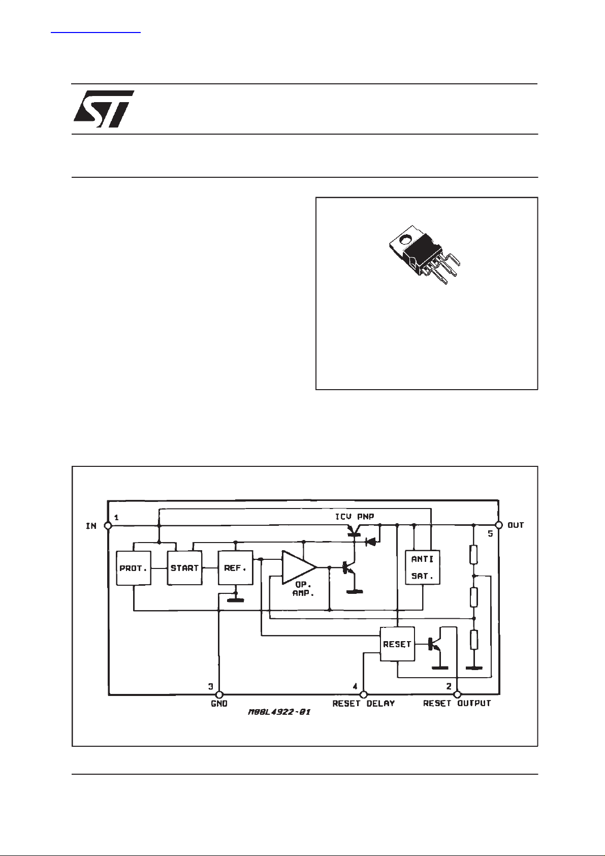
BLOCK DIAGRAM
June 2000
This is advanced informationona new product now in development or undergoing evaluation. Detailsare subjectto changewithout notice.
1/6
L4922
ABSOLUTEMAXIMUM RATINGS
Symbol Parameter Value Unit
V
V
V
T
T
T
Note: T he circuit is ESD protected according to MIL-STD-883C
THERMAL DATA
Symbol Parameter Value Unit
R
th j-case
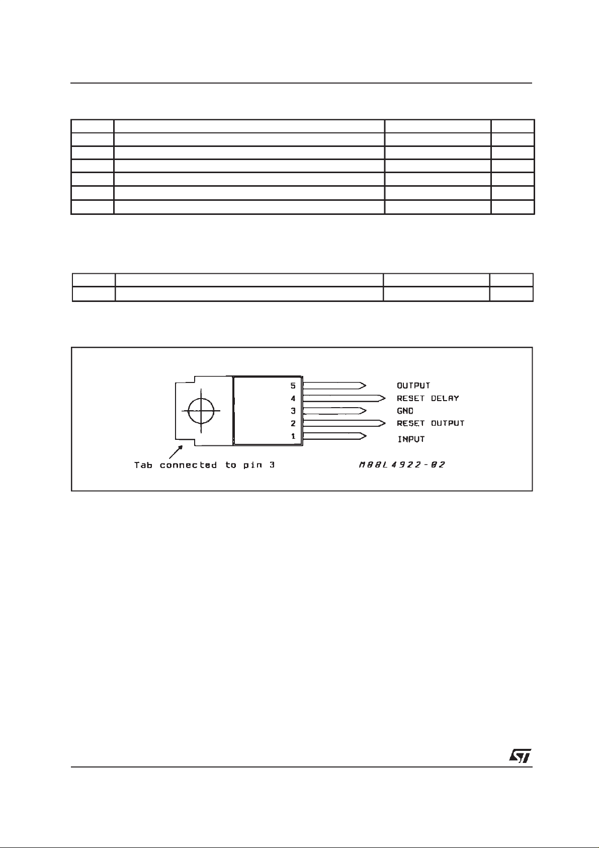
PIN CONNE CTIO N (Top view)
DC Input Voltage 35 V
i
DC Reverse Voltage –18 V
r
Positive Load Dump Protection (t = 300ms) 60 V
D
Junction Temperature Range –40 to 150 °
J
Operating Temperature Range –40 to 125 °
op
Storage Temperature Range –55 to 150
stg
Thermal Resistance Junction-case Max. 3.5
°
C
C
C
°
C/W
FUNCTI O NAL DESCRI PTION
The operatingprinciple of the voltage regulator is
basedonthereference,theerroramplifier,thedriver
and the power PNP. This stage uses an Isolated
CollectorVerticalPNPtransistorwhich allowsto obtainvery low dropoutvoltage(typ. 450mV)and low
quiescentcurrent(I
= 20mA typicallyatIo= 1A).
Q
Thanks to these featuresthe device is particularly
suited when the power dissipation must be limited
as,for example,in automotiveor industrialapplicationssuppliedby battery.
The three gain stages (operational amplifier,
driverand powerPNP) requiretheexternalcapacitor (Co
=22µF) to guaranteethe global stability
min
of the system.
2/6
Theantisaturationcircuitallowstoreducedrastically
the currentpeak whichtakes place during the start
up.
The reset function is LOW active when the output
voltagelevel islower than the resetthreshold voltageV
putvoltageis higherthanV
(typ.value:Vo–150mV).Whentheout-
RthOFF
theresetbecomes
RthON
HIGHafteradelaytimesettablewiththeexternalcapacitorC
.Typicallytd=20ms,Cd=0.1µF.Thereset
d
and delay threshold hysteresis improve the noise
immunity allowing to avoid false switchings. The
typicalresetoutputwaveformis shownin fig. 1.

L4922
ELECTRICALCHARACTERISTICS
= 14. 4V, – 40°C ≤ TJ≤ + 125°C unlessotherwisespecified)
(V
i
Symbol Parameter Test Conditions Min. Typ. Max. Unit
V
i
V
o
V
∆
Line
SVR Supply Voltage Rejection I
V
∆
LOAD
V
i–Vo
I
q
I
SC
V
R
V
RT peak
Operating Input Voltage (*) Note 1 6 26 V
Output Voltage Io= 0mA to 1A
=25°C
T
J
4.8
4.9
5.2
5.1
Line Regulation Vi= 6 to 26V; IO= 10mA 5 25 mV
= 700mA
o
f = 120Hz; C
V
= 12Vdc+5V
i
=47µF
o
pp
55 dB
Load Regulation Io= 10mA to 1A 15 50 mV
Dropout Voltage
=25°C, IO=1A
T
J
Over Full T, I
Quiescent Current Io= 10mA
=1A
I
o
= 1A 0.90 V
o
0.45 0.70 V
7
25
12
70
Short Circuit Current 1.8 A
Rset Output Saturation Voltage 1.5V< VO<V
3V < V
O<VRT (off),IR
Power On-Off Reset out Peak
1KΩReset Pull-up to V
RT (off),IR
= 1.6mA
= 8mA
O
0.65 1.0 V
0.40
0.40
Voltage
50
V
RthOFF
I
R
Reset Output Leakage Current
(high level)
t
D
Reset Pulse Delay Time CD= 100nF 20 ms
Voin Regul.
=5V
V
R
Power OFF VoThreshold Vo@ Reset out H to L
Transition; T
–40°C≤T
I
C6
Delay Capacitor Charging
V4=3V 20
=25°C
J
≤+ 125°C
J
4.75
4.70
–0.15 V
V
o
Current (current generator)
V
RthON
V
4
Power ON VoThreshold Vo@ Reset out L to H
Transition
V
rthOFF
+ 0.03V
Delay Comparator Threshold Reset out = ”1” H to L Transition 3.2 3.8 V
V
o
0.04V
–
Reset out = ”0” L to H Transition 3.7 4 4.4 V
V
6H
Delay Comparator Hysteresis 500 mV
V
V
mA
mA
V
V
µ
V
µA
V
A
(*) Note 1 : The deviceis not operatingwithin the range: 26 V < Vi<37 V.
EXTERNALCOMPENSATION
Sincethepurposeofa voltageregulatoristosupply
a fixed output voltage in spite of supply and load
variations,theopen loopgain ofthe regulatormust
be veryhigh at lowfrequencies.Thismaycauseinstability as a result of the various poles presentin
the loop. To avoid this instability dominant pole
compensationis usedtoreducephaseshiftsdueto
other poles at the unity gain frequency.The lower
thefrequencyoftheseotherpoles,thegreatermust
be the capacitorused tocreate the dominantpole
for the same DC gain.
Where the output transistor is a lateral PNP type
thereis a polein the regulationloop at a frequency
toolow to be compensatedbya capacitorwichcan
be integrated.An external compensationis thereforenecessaryso a veryhigh valuecapacitormust
be connectedfrom theoutputto ground.
Theparassiticequivalentseriesresistanceofthecapacitorusedaddsa zeroto theregulationloop.This
zero may compromise the stability of the system
sinceits effecttendsto cancelthe effectofthe pole
added.In regulatorsthisESR mustbe lessthan3Ω
and theminimumcapacitorvalue is47µF.
3/6

L4922
Figure1 : Typical ResetOutputWaveform.
Figure2 : TypicalApplicationCircuit.
(*) RECOMMENDED VALUE : C0=47µF, ESR < 10 ohm, (I
4/6
> 10 mA)OVER FULL T
out
range
.

L4922
DIM.
MIN. TYP. MAX. MIN. TYP. MAX.
mm inch
A 4.8 0.189
C 1.37
0.054
D 2.4 2.8 0.094 0.110
D1 1.2 1.35 0.047 0.053
E 0.35 0.55 0.014 0.022
E1 0.76 1.19 0.030 0.047
F 0.8 1.05 0.031 0.041
F1 1 1.4 0.039 0.055
G 3.2 3.4 3.6 0.126 0.134 0.142
G1 6.6 6.8 7 0.260 0.268 0.276
H2 10.4 0.409
H3 10.05 10.4 0.396 0.409
L 17.55 17.85 18.15 0.691 0.703 0.715
L1 15.55 15.75 15.95 0.612 0.620 0.628
L2 21.2 21.4 21.6 0.831 0.843 0.850
L3 22.3 22.5 22.7 0.878 0.886 0.894
L4 1.29 0.051
L5 2.6 3 0.102 0.118
L6 15.1 15.8 0.594
0.622
L7 6 6.6 0.236 0.260
L9 0.2 0.008
M 4.23 4.5 4.75 0.167 0.177 0.187
M1 3.75 4 4.25 0.148 0.157 0.167
V4 40°(typ.)
OUTLINE AND
MECHANICAL DATA
Pentawatt V
A
H3
B
H1
L
L1
L8
VV
C
L5
Dia.
L7
L6
D1
V1
R
D
L2
L3
RESIN BETWEEN
V3
R
R
V4
F1
LEADS
H2
E
M1
M
V4
GG1
F
L9
VV
H2
F
E1
E
V4
5/6

L4922
Information furnished is believed to be accurate and reliable. However, STMicroelectronics assumes no responsibility for the consequences of use of such information nor for any infringement of patents or other rights of third parties which may result from its use. No
license is granted by implication or otherwise under any patent or patent rights of STMicroelectronics. Specification mentioned in this
publication are subject to change without notice. This publication supersedes and replaces all information previously supplied. STMicroelectronics products are not authorized for use as critical components in life support devices or systems without express written
approval of STMicroelectronics.
Australia - Brazil - China - Finland - France - Germany - Hong Kong - India - Italy- Japan - Malaysia - Malta - Morocco -
The ST logo is a registered trademark of STMicroelectronics
2000 STMicroelectronics – Printed in Italy – All Rights Reserved
STMicroelectronics GROUP OF COMPANIES
Singapore - Spain - Sweden - Switzerland - United Kingdom - U.S.A.
http://www.st.com
6/6
 Loading...