

查询L4920供应商
L4920
VERY LOWDROP ADJUSTABLE REGULATORS
.
VERYLOWDROP VOLTAGE
.ADJUSTABLE OUTPUT VOLTAGE FROM
1.25VTO 20V
.400mAOUTPUTCURRENT
.LOWQUIESCENTCURRENT
.REVERSEVOLTAGEPROTECTION
.+ 60/ − 60VTRANSIENTPEAK VOLTAGE
PROTECTION
.SHORTCIRCUIT PROTECTION WITH FOLD-
BACKCHARACTERISTICS
.THERMAL SHUT-DOWN
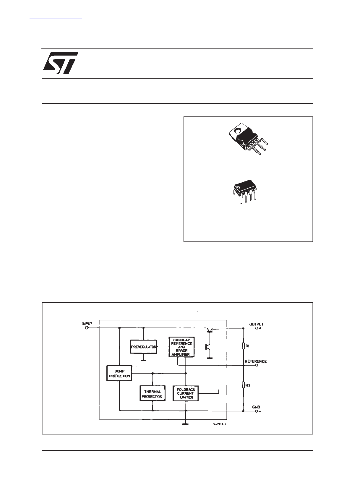
DES CRIPTION
The L4920and L4921 areadjustablevoltageregulatorswitha verylowvoltagedrop(0.4Vtyp.at 0.4A
=25°C), low quiescent current and comprehen-
T
j
siveon-chip protection.
Thesedevicesareprotectedagainstloaddumpand
field decay transients, polarity reversal and over
heating.
A foldbackcurrentlimiterprotectsagainstloadshort
circuits.
Theoutputvoltageisadjustablethroughanexternal
dividerfrom1.25V to 20V.The minimumoperating
input voltageis 5.2V (T
=25°C).
J
L4921
Pen tawatt
Minidip (4 + 4)
ORDERINGNUMBERS : L4920 (Pentawatt)
L4921(Minidip)
These regulators are designed for automotive, industrialand consumerapplicationswhere low consumptionisparticularlyimportant.
In batterybackupandstandbyapplicationsthelow
consumptionofthese devicesextendsbatterylife.
BLOCK DIAGRAM
June 2000
1/7
L4920/L4921
ABSOLUTE MAXIMUM RATINGS
Symbol Parameter Value Unit
DC Input Operating Voltage
V
i
DC Reverse Input Voltage
Transient Input Overvoltages:
Load Dump:
rise
10ms
≤
0.5
≥
Ω
5ms≤t
Fall timeconstant = 100ms
τ
f
R
SOURCE
Field Decay:
fall
10ms, R
≤
SOURCE
T
J,TSTG
5ms≤t
τ
Rise time constant = 33ms
f
Junction and Storage Temperature Range – 55 to 150
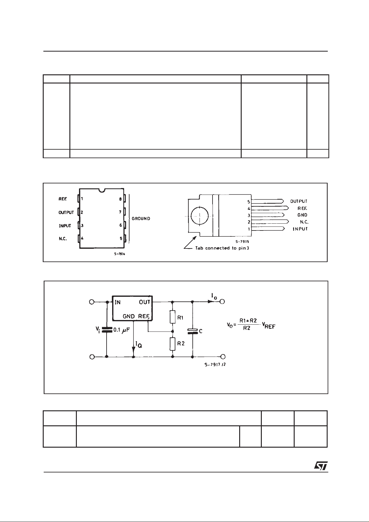
PIN CONNECTI ONS (top view)
≥10Ω
35 V
C
°
TEST AND APPLICATION CIRCUI T
C = 100µF is required for stability (ESR≤3Ωover T range)
R2 = 6.2KΩ.
THERMALDATA
Symbol Parameter Minidip
R
th j-amb
R
th j-pins
R
th j-case
Thermal Resistance Junction-ambient
Thermal Resistance Junction-pins
Thermal Resistance Junction-case
Max
Max
Max
80°C/W
15°C/W
(4 + 4)
–
Pentawatt
60°C/W
–
3.5 °C/W
2/7

L4920/L4921
ELECTRICALCHARACTERISTICS(forVI=14.4V,TJ=25°C,VO=5V,CO=100µF,unlessOtherwiseSpeci-
fied)
Symbol Parameter Test Condition Min. Typ. Max. Unit
Operating Input Voltage VO≥ 4.5V, IO= 400mA VO+0.7 26 V
V
I
V
< 4.5V, IO= 400mA 5.2 26 V
≤
O
1.20 1.25 1.30 V
≤ 400mA (*)
O
1 10 mV/V
400mA (*) V
≤
O
4.5V 3 15 mV/V
≥
O
0.05
0.2
0.4
0.4
0.7
V
V
V
V
∆V
∆
I
(* ) Foldbac k protection
Reference Voltage 5.2V < VI< 26V
REF
Line Regulation VO+1V<VI< 26V, VO≥ 4.5V
O
Load Regulation 5mA≤I
V
O
Dropout Voltage IO= 10mA
V
D
Quiescent Current IO= 0mA
I
Q
Maximal Output Current 800 mA
I
O
Short Circuit Output Current (*) 350 500 mA
OSC
V
REF
5mA ≤ I
= 5mA
I
O
= 150mA
I
O
= 400mA
I
O
+1V<VI<26V 0.8 2 mA
V
O
= 400mA (*)
I
O
V
+1V<VI<26V 65 90 mA
O
ELECTRICALCHARACTERISTICS (forVI=14.4V,–40≤ TJ≤ 125°C (note1),VO=5V,CO=100µF,unless
OtherwiseSpecified)
Symbol Parameter Test Condition Min. Typ. Max. Unit
Operating Input Voltage V
V
I
V
∆V
∆V
I
(*) Foldback protection.
Note : 1. Design limits are guaranteed (but not 100% production tested) over the indicated temperature and supply voltage
Reference Voltage 5.4V < VI< 26V 1.17 1.25 1.33 V
REF
Line Regulation VO+ 1.2V < VI< 26V, VO≥ 4.5V
O
Load Regulation 5mA ≤ IO≤ 400mA (*) VO≥ 4.5V 5 25 mV/V
O
Dropout Voltage IO= 150mA
V
D
Quiescent Current IO= 0mA
I
Q
Maximal Output Current 870 mA
I
O
Short Circuit Output Current (*) 230 500 mA
OSC
ranges. These limits are not used to calculate outgoing quality levels.
4.5V, I
≥
O
≤ VO< 4.5V, IO= 400mA 5.2 26 V
V
REF
= 400mA VO+0.9 26 V
O
2 15 mV/V
= 5mA
I
O
0.2
= 400mA
I
O
+ 1.2V < VI<26V 1,2 3 mA
V
O
= 400mA (*)
I
O
+ 1.2V < VI<26V 80 140 mA
V
O
0.4
0.4
0.7
V
V
3/7
 Loading...