


查询L4918供应商
VOLTAGE REGULATORSPLUS FILTER
.FIXEDOUTPUT VOLTAGE8.5V
.250mAOUTPUT CURRENT
.HIGH RIPPLEREJECTION
.HIGH LOADREGULATION
.HIGH LINE REGULATION
.SHORTCIRCUIT PROTECTION
.THERMALSHUTDOWN WITHHYSTERESIS
.DUMPPROTECTION
DESCRIP TIO N
TheL4918combinesbothafilterandavoltageregulatorinordertoprovidea high ripplerejectionovera
widerinput voltagerange.
A supervisorlow-passloop of theelement prevents
the outputtransistorfrom saturationat low inputvol
tages.
The non linear behaviourof this control circuitry allowsa fastsettingofthe filter.
L4918
PRELI MINA RY DATA
PENTAWATT
ORDERING NUMBER : L4918
BLOCK DIAGRAM
October1988
1/6
L4918
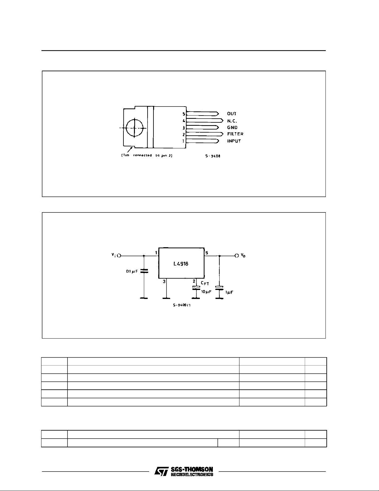
PIN CONNECTIO N (top view)
Figure 1 : Applicationand TestCircuit.
ABSOLUTE MAXIMUM RATINGS
Symbol Parameter Value Unit
Peak Input Voltage (300 ms) 40 V
V
i
DC Input Voltage 28 V
V
i
Output Current Internally Limited
I
O
Power Dissipation Internally Limited
P
tot
T
stg,Tj
Storage and Junction Temperature – 40 to 150 °C
THERMAL DATA
Symbol Parameter Value Unit
Thermal Resistance Junction-case Max 4 °C/W
2/6
R
th j-case

L4918
ELECTRICAL CHARACTERISTICS (T
=25°C;Vi= 13.5 V, unlessotherwisespecified)
amb
Symbol Parameter Test Conditions Min. Typ. Max. Unit
Input Voltage 20 V
V
i
V
O
∆V
I/O
∆V
O
∆V
O
∆V
O
I
q
∆I
q
∆V
O
Output Voltage Vi=12to18V
= 5 to 150 mA
I
O
Controlled Input-output Dropout
Voltage
Vi= 5 to 10 V
= 5 to 150 mA
I
O
Line Regulation Vi=12to18V
=10mA
I
O
Load Regulation IO= 5 to 250 mA
=30µs
t
on
= ≥ 1ms
t
off
Load Regulation
(filter mode)
Vi= 8.5 V
I
= 5 to 150 mA
O
=30µs
t
on
t
= ≥ 1ms
off
Quiescent Current IO= 5 mA 1 2 mA
Quiescent Current Change Vi= 6 to 18 V
= 5 to 150 mA
I
O
Output Voltage Drift I
= 10 mA 1.2 mV/°C
O
8.1 8.5 8.9 V
1.6 2.1 V
120mV
100 mV
150 250 mV
0.05 mA
∆T
SVR Supply Voltage Rejection V
iac
=1V
rms
f = 100 Hz
= 150 mA
I
O
V
=12to18V
IDC
= 6 to 11 V
V
IDC
Short Circuit Current 250 300 mA
I
SC
Switch On Time IO= 150 mA
t
on
T
Thermal Shutdown Junction
JSD
= 5 to 11 V
V
i
=11to18V
V
i
71
35(*)
500(*)
300
150 °C
Temperature
dB
dB
ms
ms
(*) Depending of the CFTcapacitor
PRINCI P LE OF OPERATION
Duringnormal operation (input voltage upper than
V
I MIN=VOUT NOM
+ ∆V
). The device works as a
I/O
normalvoltageregulatorbuiltaroundtheOP1ofthe
blockdiagram.
The series passelement usea PNP-NPNconnectiontoreducethedropout.Thereferencevoltageof
theOP1isderivedfromaREFthroughtheOP2and
Q3, acting as an activezener diodeof value V
REF
In this conditionthe deviceworksin the range(1)of
the characteristicof thenon lineardropcontrolunit
(seefig.2).
The output voltageis fixed to itsnominalvalue:
R1 R1
V
OUT NOM=VREF
(1 + ) = V
R2 R2
(1 + )
CFT
R1
= INTERNALLYFIXED RATIO= 2.4
R2
The ripple rejectionis quite high (71 dB)and independentfromC
FT
value.
Ontheusualvoltageregulators,whentheinputvoltage goes below the nominal value, the regulation
transistors (series element) saturate bringing the
systemout of regulationmaking it very sensibleto
everyvariationofthe inputvoltage.Onthecontrary,
.
a controlloop on the L4918 consents to avoidthe
saturationof the series element by regulating the
valueofthereferencevoltage(pin2). In fact,whenevertheinputvoltagedecreasesbelowV
pervisorloop,utilizing a nonlinear OTA,forces the
referencevoltageat pin2 to decreaseby discharging C
voltagegoes belowV
. So,duringthe staticmode, whenthe input
FT
the dropout is keptfixed
MIN
to about 1.6 V. Inthisconditionthe deviceworksas
a lowpass filterin the range(2)of theOTA charac-
IMIN
thesu-
3/6

L4918
teristic. The ripplerejection is externallyadjustable
actingon C
asfollows:
FT
SVR(jw) = =
1+
gm R1
jwC
FT
V
(jw)
I
(jw)
V
out
–6
10
(1 + )
R
2
Where:
gm = 2 .10
-5Ω-1
=OTA’S typicaltransconductance
valueon linearregion
R1
=fixed ratio
R2
Figure 2 : Nonliner TransferCharacteristicof the
DropControlUnit.
=valueof capacitorin µF
C
FT
Thereactiontimeof the supervisorloopis given by
thetransconductanceoftheOTAandbyC
.When
FT
thevalueoftheripplevoltageissohighanditsnegative peak is fast/enoughto determinean istantaneousdecreaseofthedropouttill1.2V,theOTAworks
in a highertransconductancecondition[range(3) of
the characteristic]and dischargethe capacitorrapidously.
If theripplefrequencyis highenoughthe capacitor
won’t charge itself completely,and the output voltage reaches a small value allowing a better ripple
rejection;the device’s againworking as afilter(fast
transientrange).
WithC
=10µF;f=100HzaSVRof35isobtained.
FT
Figure 3 : SupplyVoltageRejectionvs.Fre-
1) Normal oper at ing r ange (high rippl e rejection)
2) Dr op c ontrol led r ange (medi um ripple reject i on)
3) F ast discharge of C
FT
Figure 4 : Supply voltageRejectionvs.Input Volt-
age.
4/6
Figure 5 : Output Voltagevs. InputVoltage.

PENTAWATT PACKAGE MECHANICAL DATA
L4918
DIM.
mm inch
MIN. TYP. MAX. MIN. TYP. MAX.
A 4.8 0.189
C 1.37 0.054
D 2.4 2.8 0.094 0.110
D1 1.2 1.35 0.047 0.053
E 0.35 0.55 0.014 0.022
F 0.8 1.05 0.031 0.041
F1 1 1.4 0.039 0.055
G 3.4 0.126 0.134 0.142
G1 6.8 0.260 0.268 0.276
H2 10.4 0.409
H3 10.05 10.4 0.396 0.409
L 17.85 0.703
L1 15.75 0.620
L2 21.4 0.843
L3 22.5 0.886
L5 2.6 3 0.102 0.118
L6 15.1 15.8 0.594 0.622
L7 6 6.6 0.236 0.260
M 4.5 0.177
M1 4 0.157
Dia 3.65 3.85 0.144 0.152
A
H3
L
L1
C
D1
L5
Dia.
L7
L6
D
L2
L3
F1
H2
E
MM1
G1
G
F
5/6

L4918
Information furnished is believed to be accurate and reliable. However, SGS-THOMSON Microelectronics assumes no responsibility for
the consequences of use of such information nor for any infringementof patents or other rights of third parties which may result from its
use. No license is granted by implication or otherwise under any patent or patent rights of SGS-THOMSON Microelectronics. Specifications mentioned in this publication are subject to change without notice. This publication supersedes and replaces all information previously supplied. SGS-THOMSON Microelectronics products are not authorized for use as critical components in life support devices or
systems without express written approval of SGS-THOMSON Microelectronics.
1994 SGS-THOMSON Microelectronics - All Rights Reserved
Australia - Brazil - France - Germany - Hong Kong - Italy- Japan - Korea - Malaysia - Malta - Morocco - The Netherlands - Singapore-
SGS-THOMSON Microelectronics GROUP OF COMPANIES
Spain - Sweden - Switzerland - Taiwan - Thaliand - United Kingdom - U.S.A.
6/6
 Loading...