

查询L4909供应商
L4909
EXTERNALLY ADJUSTABLE MULTIFUNCTION REGULATOR
■
3 OUTPUTS
- Vo1 : output voltage variable from 5 to 12 V;
limit current : 1.2 A.
- Vo2 : output voltage variable from 5 to 12 V;
limit current : 1.2 A.
- Vo3 : output voltage variable from 5 to 12 V;
limit current : 1.2 A.
■ ENABLE INPUT FOR EACH REGULATOR
■
FEEDBACK INPUT FOR EACH REGULATOR
■
SHORT CIRCUIT PROTECTION TO GROUND
■ OVERCURRENT WARNING
■
DRIVER FOR EXTERNAL SCR (CROWBAR
PROTECTION)
■ THERMAL SHUTDOWN
DESCRIPTION
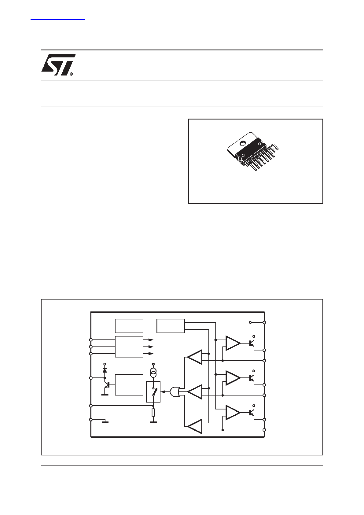
It is a monolithic Multifunction Voltage Regulator; it
contains 3 regulators, (REG1, REG2, REG3) each
one with an enable input and a feedback input, to allow the voltage setting via external resistive divider.
Each regulator is current limited and furthermore an
OR-ed warning signal is output (open collector, active low output) when the current in a regulator goes
above an over-current threshold (1 A typ for any regulator).
When one output voltage is higherthan 20% typ of its
nominal value (for instance in case of input-to-output
short circuit), the crowbar output pin is activated, triggering an external SCR (connected between input
and ground) that blows the input line fuse.
MULTIWATT15
BLOCKDIAGRAM
EN1
EN2
EN3
OC
TRIG
GND
May 2000
THERMAL
SHUTDOWN
6
7
9
5
4
8
ENABLE
CONTROL
OVER
CURRENT
CHECK
REFERENCE
GENERATOR
REG1
REG2
REG3
++
REF
REF+20%
+
+
+
+
+
+
REG1
-
REG2
-
REG3
-
+
3,13
+
+
14
15
+
11
10
D00AU1171
V
INA,VINB
2
V
O1
1
FB1
V
O2
FB2
V
O3
FB3
1/7
L4909
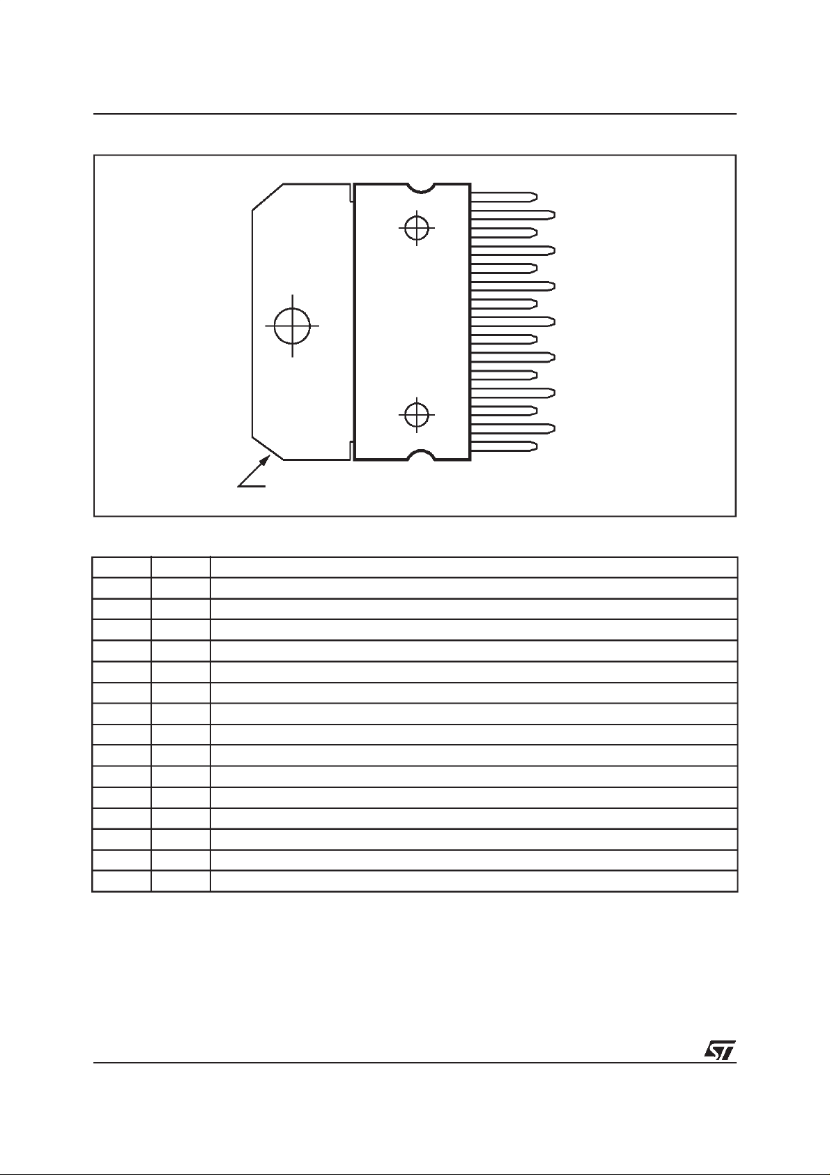
PIN CONNECTION
15
14
13
12
11
10
9
8
7
6
5
4
3
2
1
TAB CONNECTEDTO PIN 8
Table 1. Pin Description
No. Pin Name Function
1 FB1 REG1 feedback voltage input
2 Vo1 REG1 output voltage
3 VinA Input DC supply voltage
4 TRIG Trigger for external SCR (crowbar protection)
5 OC Over current warning output
6 EN1 REG1 enable input
7 EN2 REG2 enable input
8 GND Analog ground
9 EN3 REG3 enable input
10 FB3 REG3 feedback voltage input
11 Vo3 REG3 output voltage
12 N.C. Not Connected
13 VinB Input DC supply voltage
14 Vo2 REG2 output voltage
15 FB2 REG2 feedback voltage input
D00AU1153
FB2
V
O2
V
INB
N.C.
V
O3
FB3
EN3
GND
EN2
EN1
OC
TRIG
V
INA
V
O1
FB1
2/7
ABSOLUTEMAXIMUMRATINGS
Symbol Parameter Value Unit
Vin VinA,VinB input DC supply voltage 40 V
Io Vo1, Vo2, Vo3 output currents internally limited
Voc OC output voltage min (15, Vin) V
VENx ENx input voltage 15 V
Top Operating temperature range 0 to 70
Tstg Storage temperature - 40 to 150
THERMAL DATA
Symbol Parameter Value Unit
L4909
o
C
o
C
R
TH j-case
ELECTRICAL CHARACTERISTICS (C
Thermal Resistance Junction to Case 1.8 °C/W
= 100nF; Vin-Vo=5V;Io=10mA;T
out
=25°C unless otherwise
case
specified
Symbol Parameter Test Condition Min. Typ. Max. Unit
Vo1 REG1 output voltage range 5 12 V
V(FB1) REG1 feedback voltage EN1=ON; 1.22 1.27 1.32 V
Ilim1 REG1 output current limit EN1=ON; Vin-Vo1<12V 1.20 1.70 A
V
∆
-------------
V
∆ V
-------------
V
line regulation Io1=10mA; Vin-Vo1=3 to 25V
o1
o1
load regulation Io1=10 mA to 1.2A
o1
o1
Io1=10mA; Vin-Vo1=3 to 12V
Io1=10 mA to 0.5A
Vd1 REG1 drop out Io1=500mA 2.20 V
SVR1 REG1 supply voltage rejec. freq=120 Hz to 1KHz 60 dB
Vo2 REG2 output voltage range 5 12 V
V(FB2) REG2 feedback voltage EN2 = ON; 1.22 1.27 1.32 V
0.6
0.1
0.5
0.1
2%
2%
Ilim2 REG2 output current limit EN2=ON; Vin-Vo2<12V 1.20 1.70 A
∆ V
-------------
V
o2
∆ V
-------------
V
o2
line regulation Io2=10mA;Vin-Vo2=3 to 25 V
o2
load regulation Io2=10 mA to 1.2A
o2
Io2=10mA;Vin-Vo2=3 to 12 V
Io2=10 mA to 0.5A
0.6
0.1
0.5
0.1
2%
2%
Vd2 REG2 drop out Io2=500mA 2.2 V
3/7

L4909
ELECTRICAL CHARACTERISTCS
(continued)
Symbol Parameter Test Condition Min. Typ. Max. Unit
SVR2 REG2 supply voltage rejec. freq=120 Hz to 1KHz 60 dB
Vo3 REG3 output voltage range 5 12 V
V(FB3) REG3 feedback voltage EN3=ON; 1.22 1.27 1.32 V
Ilim3 REG3 output current limit EN3=ON; Vin-Vo3<12V 1.20 1.70 A
∆V
-------------
V
o3
∆ V
-------------
V
o3
line regulation Io3=10mA; Vin-Vo3=3 to 25V
o3
load regulation Io3=10 mA to 1.2A
o3
Io3=10mA; Vin-Vo3=3 to 12V
Io3=10 mA to 0.5A
0.6
0.1
0.5
0.1
2%
2%
Vd3 REG3 drop out Io3=500mA 2.20 V
SVR3 REG3 supply voltage rejec. freq=120 Hz to 1KHz 60 dB
ENx enable input voltage
(active high)
STAND_BY
ON 3.5
0.8 V
Istby current consumption in stand_by EN1=EN2=EN3≤0.5 V 20 µA
ITRIG current at TRIG output SCR trigger circuit in ON state;
25 mA
V(TRIG) = 2V
V
ZTRIG TRIG to GND impedance SCR trigger circuit in OFF state 0.2 KΩ
V(FB)_TR FBx voltage fortrigger SCR on any regulator 1.52 V
I(FB) Feedback’s input current any regulator 2 µA
I(EN) EN’s input current V(EN) = 5V 160 µA
Ion current consumption in ON state
(current in the exter nalfeedbackresistors not
included)
V_OC_L current_warning output
voltage
I_OC_H current_warning leakage no warning conditions
one regulator ON; Vo= 12V
two regulators ON; Vo = 12V
three regulators ON; Vo = 12V
warning conditions
Isink < 3 mA
11
20
29
mA
0.40 V
1 µA
V(OC) = 15V
I_oc/Ilim warning threshold current / limit
current
any regulator
Vin - Vout<12V
0.6
4/7

L4909
The current protection is a function of the Vce, i.e. the drop between input and output voltages (Vin-Vo). The
shape of that relationship is shown in following figure 1.
Figure 1.
Figure 2. REGULATOR TYPICAL APPLICATION
FROM
RECTIFIER
ULTRAFAST FUSE
V
INA
+5V
330nF
4.7K
PULL-UP
RESISTOR
(*) It is possible toenable the regulatorsconnecting the ENxpins to Vinthrough a 25KΩ
Suggested valueforRAxis 1.2KΩ
Thevalue of RBxmustbe choosen, depending onthe desiredoutput voltage V
V
ox
RBx=R
-1
Ax
1.27
(*)EN1
(*)EN2
(*)EN3
OC
TRIG
3
6
7
9
5
4
GND
V
INB
13
V
O1
2
V
O2
14
V
O3
11
R
B3RB2RB1
FB1
1
FB2
15
FB3
12
following the
ox?
RA3RA2R
8
100µF
A1
formula:
100µF
100nFSCR
D00AU1154
100µF
100nF
100nF
5/7

L4909
DIM.
MIN. TYP. MAX. MIN. TYP. MAX.
A 5 0.197
B 2.65 0.104
C 1.6 0.063
D 1 0.039
E 0.49 0.55 0.019 0.022
F 0.66 0.75 0.026 0.030
G 1.02 1.27 1.52 0.040 0.050 0.060
G1 17.53 17.78 18.03 0.690 0.700 0.710
H1 19.6 0.772
H2 20.2 0.795
L 21.9 22.2 22.5 0.862 0.874 0.886
L1 21.7 22.1 22.5 0.854 0.870 0.886
L2 17.65 18.1 0.695 0.713
L3 17.25 17.5 17.75 0.679 0.689 0.699
L4 10.3 10.7 10.9 0.406 0.421 0.429
L7 2.65 2.9 0.104 0.114
M 4.25 4.55 4.85 0.167 0.179 0.191
M1 4.63 5.08 5.53 0.182 0.200 0.218
S 1.9 2.6 0.075 0.102
S1 1.9 2.6 0.075 0.102
Dia1 3.65 3.85 0.144 0.152
mm inch
OUTLINEAND
MECHANICALDATA
Multiwatt15 V
6/7

L4909
Information furnished is believed to be accurate and reliable. However, STMicroelectronics assumes no responsibility for the consequences
of useofsuch information nor for anyinfringement ofpatents or otherrightsofthird partieswhichmayresultfrom its use. No license is granted
by implication or otherwise under any patent or patent rights of STMicroelectronics. Specifications mentioned in this publication are subject
to change without notice. This publication supersedes and replaces all information previously supplied. STMicroelectronics products are not
authorized for use as critical components in life support devices or systems without express written approval of STMicroelectronics.
The ST logo is a registered trademark of STMicroelectronics
2000 STMicroelectronics - All Rights Reserved
Australia - Brazil - China - Finland - France - Germany - Hong Kong - India - Italy - Japan - Malaysia - Malta - Morocco - Singapore - Spain
STMicroelectronics GROUP OF COMPANIES
- Sweden - Switzerland - United Kingdom - U.S.A.
http://www.st.com
7/7
 Loading...