

查询L4904A供应商
DUAL5V REGULATOR WITH RESET
.
OUTPUTCURRENTS : I01=50mA
I
=100mA
02
.
FIXEDPRECISIONOUTPUTVOLTAGE
±
5V
2%
.
RESETFUNCTION CONTROLLED BY INPUT
VOLTAGEAND OUTPUT 1 VOLTAGE
.
RESET FUNCTION EXTERNALLY PROGRAMMABLETIMING
.
RESETOUTPUT LEVELRELATEDTO
OUTPUT2
.
OUTPUT 2 INTERNALLY SWITCHED WITH
ACTIVEDISCHARGING
.
LOW LEAKAGE CURRENT, LESS THAN 1µA
ATOUTPUT 1
.
LOWQUIESCENTCURRENT (Input 1)
.
INPUT OVERVOLTAGE PROTECTION UP TO
60V
.
RESETOUTPUT NORMALLY HIGH
.
OUTPUTTRANSISTORSSOAPROTECTION
.
SHORT CIRCUIT AND THERMAL OVERLOADPROTECTION
Minidip
ORDERING NUMBER :
L4904A
L4904A
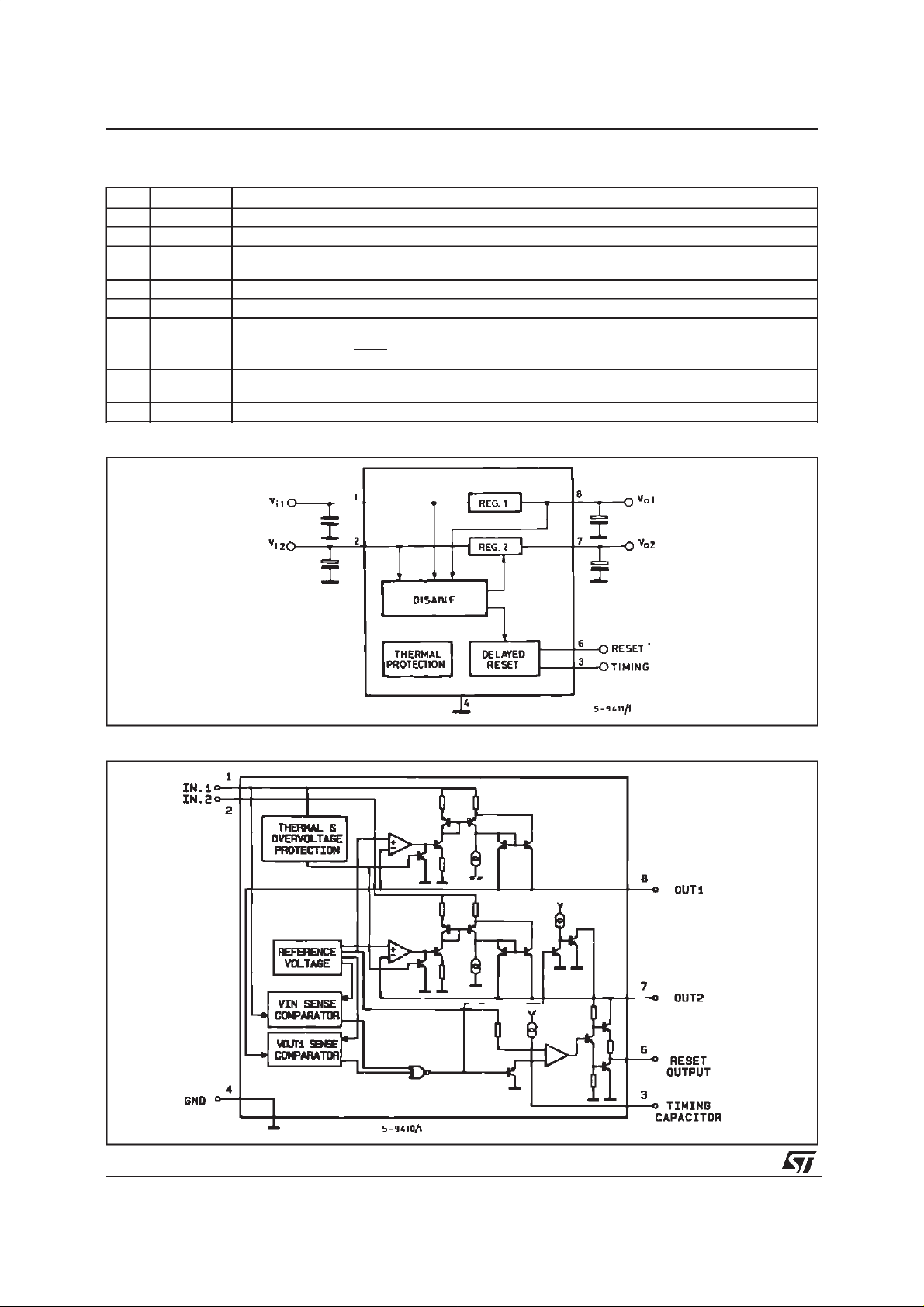
DESCRIPTION
The L4904A is a monolithic low drop dual 5V
regulatordesignedmainlyforsupplyingmicroprocessorsystems.
Resetand data savefunctionsduring switchon/off
canbe realized.
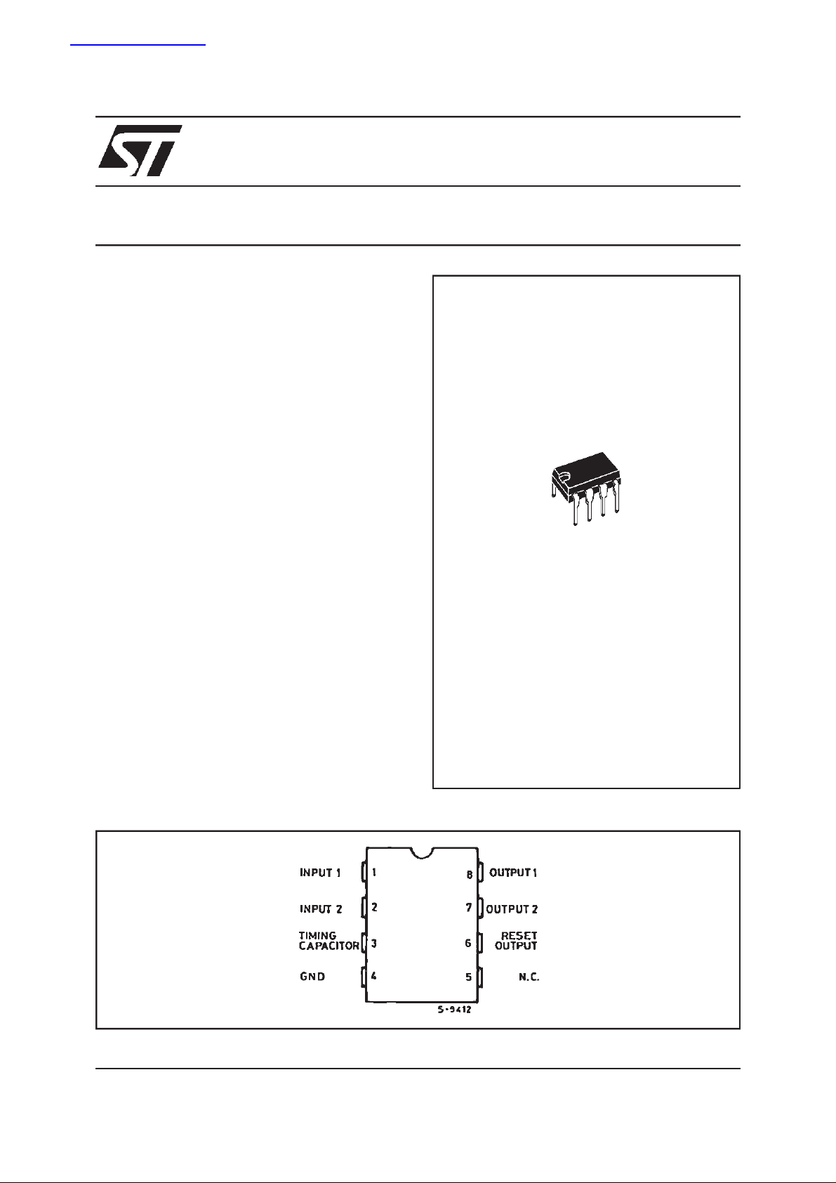
PIN CONNECTION
June 2000
1/9
L4904A
PIN FUNCTIONS
N°
1 Input 1 Low Quiescent Current 50mA Regulator Input.
2 Input 2 100mA Regulator Input.
3 Timing
4 GND Common Ground.
5 N.C. Not connected.
6 Reset
7 Output 2 5V – 100mA Regulator Output. Enabled if V
8 Output 1 5V – 50mA regulator output with low leakage in switch-OFF condition.
BLOCKDIAGRAM
Name Function
If Reg. 2 is switching-ON the delay capacitor is charged with a 10µA constant current. When
Capacitor
Reg. 2 is switched-OFF the delay capacitor is discharged.
When pin 3reaches 5V the reset output is switchedhigh.
Output
Therefore t
the C
capacitor is discharged.
o2
RD=Ct
5V
(
); tRD(ms) = Ct(nF).
10µA
1>VRTand V
o
IN 2>VIT
. If Reg. 2 is switched-OFF
SCHEMATIC DIAGRAM
2/9
ABSOLUTEMAXIMUM RATINGS
Symbol Parameter Value Unit
V
IN
I
o
P
tot
T
DC Input Voltage
Transient Input Overvoltage (t = 40ms)
Output Current Internally Limited
Power Dissipation at T
Storage and Junction Temperature – 40 to 150
j
amb
=50°C
24
60
1W
THERMALDATA
Symbol Parameter Value Unit
R
th j-amb
Thermal ResistanceJunction-ambient Max 100
L4904A
V
V
°C
°C/W
ELECTRICAL CHARACTERISTICS
(V
IN
= 14.4V,T
=25oC unlessotherwise specified)
amb
Symbol Parameter Test Conditions Min. Typ. Max. Unit
V
DC Operating Input Voltage 20 V
i
V
Output Voltage1
01
V
V
V
V
∆V
∆
∆
∆
Output Voltage2 HIGH
02 H
Output Voltage2 LOW I02= – 5mA 0.1 V
02 L
I
Output Current 1 ∆
01
I
Leakage Output 1 Current
L01
I
Output Current 2 ∆
02
Output 1 Dropout Voltage (*) I01= 10mA
I01
V
Input Threshold Voltage V01+ 1.2 6.4 V01+ 1.7 V
IT
Input Threshold Voltage Hyst. 250 mV
ITH
Line Regulation 7V < VIN< 18V, I01= 5mA 5 50 mV
01
Line Regulation 2 7V < VIN< 18V, I02= 5mA 5 50 mV
V
02
Load Regulation 1 VIN= 8V, 5mA < I01< 50mA 5 20 mV
V
01
Load Regulation 2 VIN= 8V, 5mA < I02< 100mA 10 50 mV
V
02
IQ Quiescent Current
Quiescent Current 1 6.3V < V
I
Q1
V
V
V
V
∆V
∆
S
S
* The dropout voltage is defined as the differencebetween the input and the output voltage when the output voltage is lowered of 25 mV under
constant output current condition.
Reset Threshold Voltage V02–0.15 4.9 V02– 0.05 V
RT
Reset Threshold Hysteresis 30 50 80 mV
RTH
Reset Output Voltage HIGH
RH
Reset Output Voltage LOW IR= – 5mA 0.25 0.4 V
RL
t
Reset Pulse Delay Ct= 10nF 3 11 ms
RD
t
Timing Capacitor Discharge
d
Time
01
Thermal Drift
T
∆
V
02
Thermal Drift – 20°C≤<0>T
∆T
Supply Voltage Rejection f = 100Hz, VR= 0.5V, Io= 50mA 50 84 dB
VR1
Supply Voltage Rejection f = 100Hz, VR= 0.5V, Io= 100mA 50 80 dB
VR2
R Load 1kΩ
R Load 1kΩ
= – 100mV
V
01
=0,V01≤ 3V
V
IN
= – 100mV
V
02
= 50mA
I
01
I
02=I01
0<V
7V < V
I
01
I
R
5mA
≤
< 13V
IN
< 13V
IN
< 13V, V
IN1
≤ 5mA, I02=0
= 500µA
IN2
=0
Ct= 10nF 20
–20°C≤<0>T
amb
amb
≤ 125°C
125°C
≤
4.95 5.05 5.15 V
V01–0.1 5 V
01
50 mA
1
100 mA
0.7
0.75
4.5
1.6
0.8
0.9
6.5
3.5
0.6 0.9 mA
V
– 1 4.12 V
02
02
0.3
–0.8
0.3
– 0.8
V
µA
V
V
mA
V
µs
mV/°C
mV/°C
3/9
 Loading...