

查询L4903供应商
WITH RESET AND DISABLE FUNCTIONS
.
OUTPUTCURRENTS : I01= 50mA
I
=100mA
02
.
FIXEDPRECISION OUTPUT VOLTAGE
5V ± 2%
.
RESETFUNCTION CONTROLLED BY INPUT
VOLTAGEANDOUTPUT1VOLTAGE
.
RESET FUNCTION EXTERNALLY PROGRAMMABLETIMING
.
RESET OUTPUT LEVEL RELATED TO OUTPUT2
.
OUTPUT 2 INTERNALLY SWITCHED WITH
ACTIVEDISCHARGING
.
OUTPUT2DISABLELOGICALINPUT
.
LOW LEAKAGECURRENT, LESS THAN 1µA
ATOUTPUT1
.
INPUTOVERVOLTAGEPROTECTIONUP TO
60V
.
RESETOUTPUT NORMALLYLOW
.
OUTPUTTRANSISTORS SOAPROTECTION
.
SHORT CIRCUIT AND THERMAL OVERLOADPROTECTION
L4903
DUAL 5V REGULATOR
PRELIMINARY DATA
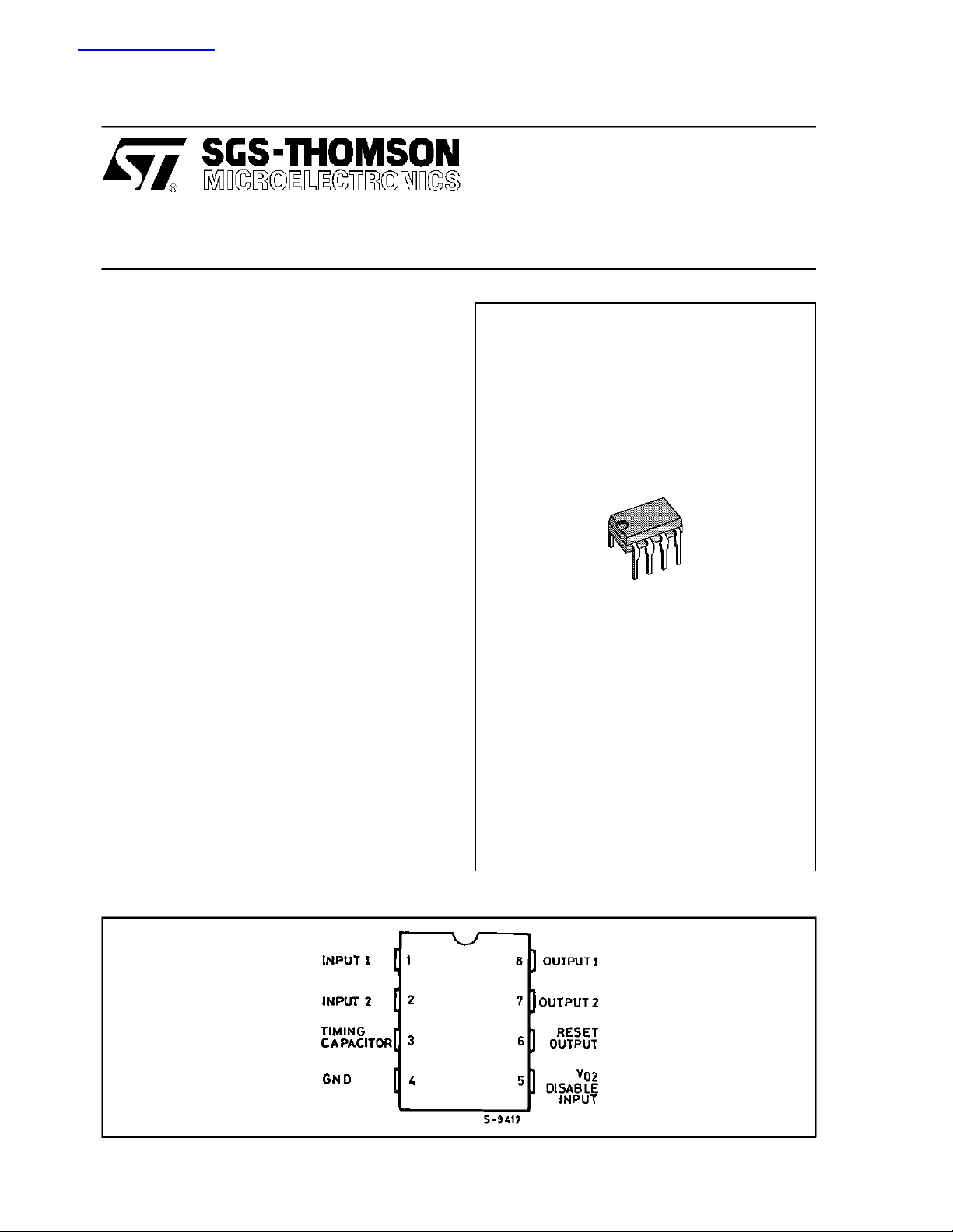
Minidip
ORDERING NUMBERS : L4903
DESCRIPTION
TheL4903 is a monolithic low dropdual 5 V regulatordesignedmainlyforsupplyingmicroprocessor
systems.
Reset, data save functions and remote switch
on/off controlcan be realized.
PIN CONNECTION
July1993
1/8
L4903
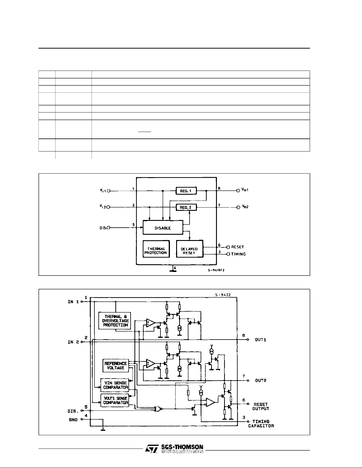
PIN FUNCTIONS
N° Name Function
1 Input1 Low Quiescent Current 50mA Regulator Input
2 Input2 100mA Regulator Input.
3 Timing
Capacitor
4 GND Common Ground
5 Disable Input A high level (> V
6 Reset Output When pin 3 reaches 5V the reset output is switched low.
7 Output 2 5V – 100mARegulator Output. Enabled if V
8 Output 1 5V– 50mA regulator output with low leakage inswitch-OFF condition.
BLOCKDIAGRAM
If Reg. 2 is switched-ON the delay capacitor is charged with a 10µA constant current. When
Reg. 2 is switched-OFF the delaycapacitor isdischarged.
) disables output Reg. 2.
DT
5V
(
Therefore t
RD=Ct
If Reg. 2 is switched-OFF the C
);tRD(ms) = Ct(nF).
10µA
02
1>VRT. DISABLE INPUT < VDTand V
capacitor is discharged.
o
IN 2>VIT
.
SCHEMATIC DIAGRAM
2/8
ABSOLUTE MAXIMUMRATINGS
Symbol Parameter Value Unit
V
IN
V
P
tot
T
stg,Tj
DC Input Voltage 24 V
Transient Input Overvoltage (t =40ms) 60 V
t
Power Dissipation at T
=50°C1W
amb
Storage and Junction Temperature – 40 to 150 °C
THERMALDATA
Symbol Parameter Value Unit
R
th (j-pin)
R
th (j-a)
Thermal Resistance Junction-pin 4 Max. 70 °C/W
Thermal Resistance Junction-ambient Max. 100 °C/W
L4903
ELECTRICALCHARACTERISTICS (VIN= 14.4V,T
=25oC unless otherwise specified)
amb
Symbol Parameter Test Conditions Min. Typ. Max. Unit
V
V
V
02 H
V
02 L
I
01
I
L01
I
02
V
I01
V
V
ITH
∆V
∆V
∆V
∆V
IQ Quiescent Current I
I
Q1
V
RT
V
RTH
V
RH
V
RL
t
RD
t
V
DT
I
D
∆V
01
,
∆T
SVR1 Supply Voltage Rejection f = 100Hz, V
SVR2 Supply Voltage Rejection f = 100Hz, V
T
JSD
*The dropoutvoltage is defined as the difference between the input andthe output voltage when the output voltage is lowered of 25 mV under
constant output current condition.
DC Operating Input Voltage 20 V
i
Output Voltage 1 R Load 1kΩ 4.95 5.05 5.15 V
01
Output Voltage 2 HIGH R Load 1kΩ V01–0.1 5 V
Output Voltage 2 LOW I02= – 5mA 0.1 V
Output Current 1 max.(*) ∆V01= – 100mV 50 mA
Leakage Output 1 Current VIN=0,V01≤ 3V 1 µA
Output Current 2 max.(*) ∆V02= – 100mV 100 mA
Output 1 Dropout Voltage (*) I01= 10mA
= 50mA
I
01
Input Threshold Voltage V01+ 1.2 6.4 V01+ 1.7 V
IT
0.7
0.75
Input Threshold Voltage Hyst. 250 mV
Line Regulation 1 7V < VIN< 18V, I01= 5mA 5 50 mV
01
Line Regulation 2 7V < VIN< 18V, I02= 5mA 5 50 mV
02
Load Regulation 1 V
01
Load Regulation 2 V
02
Quiescent Current 1 6.3V < V
= 8V, 5mA < I01< 50mA 5 20 mV
IN1
= 8V, 5mA < I02< 100mA 10 50 mV
IN1
≤ 5mA
01=I02
< 13V
0<V
IN
7V < V
7V < V
I
01
< 13V V02LOW
IN
< 13V V02HIGH
IN
IN1
≤5mA, I02=0
< 13V, V
IN2
=0
4.5
2.7
1.6
0.6 0.9 mA
Reset Threshold Voltage V02– 0.04 4.7 V02– 0.02 V
Reset Threshold Hysteresis 30 50 80 mV
Reset Output Voltage HIGH IR= 500µAV
– 1 4.12 V
02
Reset Output Voltage LOW IR= – 5mA 0.25 0.4 V
Reset Pulse Delay Ct= 10nF 3 5 11 ms
Timing Capacitor Discharge
d
Time
Ct= 10nF 20 µs
V02DisableThreshold Voltage 1.25 2.4 V
V02DisableInput Current VD≤ 0.4V
∆V
02
Thermal Drift – 20°C ≤ T
∆T
≥ 2.4V
V
D
100mA
≤125°C
amb
= 0.5V, Io = 50mA 50 84 dB
R
= 0.5V, Io=
R
50 80 dB
-150
30
0.3
- 0.8
Thermal Shut Down 150 °C
0.8
0.9
6.5
4.5
3.5
01
V
V
V
mA
02
V
µA
µA
mV/°C
3/8
 Loading...