

Features
LGA-16
(3x3x1 mm)
■ Wide supply voltage, 2.2 V to 3.6 V
■ Wide extended operating temperature range
(from -40 °C to 85 °C)
■ Low voltage compatible IOs, 1.8 V
■ Low power consumption
■ Embedded power-down
■ Sleep mode
■ Fast turn-on and wake-up
■ Three selectable full scales up to 2000 dps
■ 16 bit rate value data output
■ 8 bit temperature data output
2
■ I
C/SPI digital output interface
■ 2 dedicated lines (1 interrupt, 1 data ready)
■ User enable integrated high-pass filters
■ Embedded temperature sensor
■ Embedded 32 levels of 16 bit data output FIFO
■ High shock survivability
■ ECOPACK
®
RoHS and “Green” compliant
Applications
■ Gaming and virtual reality input devices
■ Motion control with MMI (man-machine
interface)
■ GPS navigation systems
■ Appliances and robotics
L3GD20H
MEMS motion sensor:
three-axis digital output gyroscope
Datasheet — preliminary data
Description
The L3GD20H is a low-power three-axis angular
rate sensor.
It includes a sensing element and an IC interface
able to provide the measured angular rate to the
external world through digital interface (I
The sensing element is manufactured using a
dedicated micromachining process developed by
ST to produce inertial sensors and actuators on
silicon wafers.
The IC interface is manufactured using a CMOS
process that allows a high level of integration to
design a dedicated circuit which is trimmed to
better match the sensing element characteristics.
The L3GD20H has a full scale of
±245/±500/±2000 dps and is capable of
measuring rates with a user selectable
bandwidth.
The L3GD20H is available in a plastic land grid
array (LGA) package and can operate within a
temperature range from -40 °C to +85 °C.
2
C/SPI).
Table 1. Device summary
Order code Temperature range (°C) Package Packing
L3GD20H -40 to +85 LGA-16 (3x3x1) Tray
L3GD20HTR -40 to +85 LGA-16 (3x3x1) Tape and reel
July 2012 Doc ID 023469 Rev 1 1/25
This is preliminar y information on a new product now in development or undergoing evaluation. Details are subject to
change without notice.
www.st.com
25

Contents L3GD20H
Contents
1 Block diagram and pin description . . . . . . . . . . . . . . . . . . . . . . . . . . . . . 5
1.1 Pin description . . . . . . . . . . . . . . . . . . . . . . . . . . . . . . . . . . . . . . . . . . . . . . 5
2 Mechanical and electrical specifications . . . . . . . . . . . . . . . . . . . . . . . . 7
2.1 Mechanical characteristics . . . . . . . . . . . . . . . . . . . . . . . . . . . . . . . . . . . . . 7
2.2 Electrical characteristics . . . . . . . . . . . . . . . . . . . . . . . . . . . . . . . . . . . . . . . 8
2.3 Temperature sensor characteristics . . . . . . . . . . . . . . . . . . . . . . . . . . . . . . 9
2.4 Communication interface characteristics . . . . . . . . . . . . . . . . . . . . . . . . . 10
2.4.1 SPI - serial peripheral interface . . . . . . . . . . . . . . . . . . . . . . . . . . . . . . . 10
2.4.2 I2C - Inter IC control interface . . . . . . . . . . . . . . . . . . . . . . . . . . . . . . . . 11
2.5 Absolute maximum ratings . . . . . . . . . . . . . . . . . . . . . . . . . . . . . . . . . . . . 12
2.6 Terminology . . . . . . . . . . . . . . . . . . . . . . . . . . . . . . . . . . . . . . . . . . . . . . . 13
2.6.1 Sensitivity . . . . . . . . . . . . . . . . . . . . . . . . . . . . . . . . . . . . . . . . . . . . . . . . 13
2.6.2 Zero-rate level . . . . . . . . . . . . . . . . . . . . . . . . . . . . . . . . . . . . . . . . . . . . 13
2.7 Soldering information . . . . . . . . . . . . . . . . . . . . . . . . . . . . . . . . . . . . . . . . 13
3 Digital main blocks . . . . . . . . . . . . . . . . . . . . . . . . . . . . . . . . . . . . . . . . . 14
3.1 Block diagram . . . . . . . . . . . . . . . . . . . . . . . . . . . . . . . . . . . . . . . . . . . . . . 14
3.2 FIFO . . . . . . . . . . . . . . . . . . . . . . . . . . . . . . . . . . . . . . . . . . . . . . . . . . . . . 14
4 Digital interfaces . . . . . . . . . . . . . . . . . . . . . . . . . . . . . . . . . . . . . . . . . . . 15
4.1 I2C serial interface . . . . . . . . . . . . . . . . . . . . . . . . . . . . . . . . . . . . . . . . . . 15
4.1.1 I2C operation . . . . . . . . . . . . . . . . . . . . . . . . . . . . . . . . . . . . . . . . . . . . . 16
4.2 SPI bus interface . . . . . . . . . . . . . . . . . . . . . . . . . . . . . . . . . . . . . . . . . . . 17
4.2.1 SPI read . . . . . . . . . . . . . . . . . . . . . . . . . . . . . . . . . . . . . . . . . . . . . . . . . 19
4.2.2 SPI write . . . . . . . . . . . . . . . . . . . . . . . . . . . . . . . . . . . . . . . . . . . . . . . . 20
4.2.3 SPI read in 3-wires mode . . . . . . . . . . . . . . . . . . . . . . . . . . . . . . . . . . . 21
5 Package information . . . . . . . . . . . . . . . . . . . . . . . . . . . . . . . . . . . . . . . . 22
6 Revision history . . . . . . . . . . . . . . . . . . . . . . . . . . . . . . . . . . . . . . . . . . . 24
2/25 Doc ID 023469 Rev 1

L3GD20H List of tables
List of tables
Table 1. Device summary . . . . . . . . . . . . . . . . . . . . . . . . . . . . . . . . . . . . . . . . . . . . . . . . . . . . . . . . . . 1
Table 2. Pin description . . . . . . . . . . . . . . . . . . . . . . . . . . . . . . . . . . . . . . . . . . . . . . . . . . . . . . . . . . . 6
Table 3. Mechanical characteristics . . . . . . . . . . . . . . . . . . . . . . . . . . . . . . . . . . . . . . . . . . . . . . . . . . 7
Table 4. Electrical characteristics . . . . . . . . . . . . . . . . . . . . . . . . . . . . . . . . . . . . . . . . . . . . . . . . . . . . 8
Table 5. Temperature sensor characteristics . . . . . . . . . . . . . . . . . . . . . . . . . . . . . . . . . . . . . . . . . . . 9
Table 6. SPI slave timing values. . . . . . . . . . . . . . . . . . . . . . . . . . . . . . . . . . . . . . . . . . . . . . . . . . . . 10
Table 7. I2C slave timing values. . . . . . . . . . . . . . . . . . . . . . . . . . . . . . . . . . . . . . . . . . . . . . . . . . . . 11
Table 8. Absolute maximum ratings . . . . . . . . . . . . . . . . . . . . . . . . . . . . . . . . . . . . . . . . . . . . . . . . . 12
Table 9. Serial interface pin description . . . . . . . . . . . . . . . . . . . . . . . . . . . . . . . . . . . . . . . . . . . . . . 15
Table 10. I2C terminology. . . . . . . . . . . . . . . . . . . . . . . . . . . . . . . . . . . . . . . . . . . . . . . . . . . . . . . . . . 15
Table 11. SAD+Read/Write patterns . . . . . . . . . . . . . . . . . . . . . . . . . . . . . . . . . . . . . . . . . . . . . . . . . 16
Table 12. Transfer when Master is writing one byte to slave . . . . . . . . . . . . . . . . . . . . . . . . . . . . . . . 16
Table 13. Transfer when Master is writing multiple bytes to slave . . . . . . . . . . . . . . . . . . . . . . . . . . . 17
Table 14. Transfer when Master is receiving (reading) one byte of data from slave . . . . . . . . . . . . . 17
Table 15. Transfer when Master is receiving (reading) multiple bytes of data from slave . . . . . . . . . 17
Table 16. LGA 3x3x1.0 16L mechanical data. . . . . . . . . . . . . . . . . . . . . . . . . . . . . . . . . . . . . . . . . . . 22
Table 17. Document revision history . . . . . . . . . . . . . . . . . . . . . . . . . . . . . . . . . . . . . . . . . . . . . . . . . 24
Doc ID 023469 Rev 1 3/25

List of figures L3GD20H
List of figures
Figure 1. Block diagram . . . . . . . . . . . . . . . . . . . . . . . . . . . . . . . . . . . . . . . . . . . . . . . . . . . . . . . . . . . . 5
Figure 2. Pin connection . . . . . . . . . . . . . . . . . . . . . . . . . . . . . . . . . . . . . . . . . . . . . . . . . . . . . . . . . . . 5
Figure 3. SPI slave timing diagram . . . . . . . . . . . . . . . . . . . . . . . . . . . . . . . . . . . . . . . . . . . . . . . . . . 10
Figure 4. I2C slave timing diagram . . . . . . . . . . . . . . . . . . . . . . . . . . . . . . . . . . . . . . . . . . . . . . . . . . 11
Figure 5. Block diagram . . . . . . . . . . . . . . . . . . . . . . . . . . . . . . . . . . . . . . . . . . . . . . . . . . . . . . . . . . . 14
Figure 6. Read and write protocol . . . . . . . . . . . . . . . . . . . . . . . . . . . . . . . . . . . . . . . . . . . . . . . . . . . 18
Figure 7. SPI read protocol . . . . . . . . . . . . . . . . . . . . . . . . . . . . . . . . . . . . . . . . . . . . . . . . . . . . . . . . 19
Figure 8. Multiple bytes SPI read protocol (2 bytes example) . . . . . . . . . . . . . . . . . . . . . . . . . . . . . . 19
Figure 9. SPI write protocol . . . . . . . . . . . . . . . . . . . . . . . . . . . . . . . . . . . . . . . . . . . . . . . . . . . . . . . . 20
Figure 10. Multiple bytes SPI write protocol (2 bytes example) . . . . . . . . . . . . . . . . . . . . . . . . . . . . . . 20
Figure 11. SPI read protocol in 3-wires mode . . . . . . . . . . . . . . . . . . . . . . . . . . . . . . . . . . . . . . . . . . . 21
Figure 12. LGA 3x3x1.0 16L mechanical drawing . . . . . . . . . . . . . . . . . . . . . . . . . . . . . . . . . . . . . . . . 23
4/25 Doc ID 023469 Rev 1
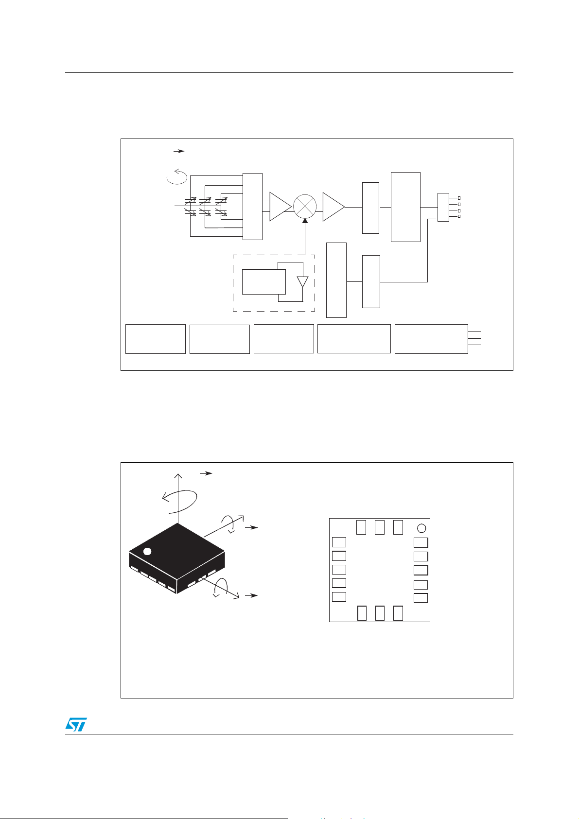
L3GD20H Block diagram and pin description
FIFO
TRIMMING
CIRCUITS
REFERENCE
MIXER
CHARGE
AMP
CLOCK
LOW-PASS
FILTER
+ Ω
x,y,z
I2C
SPI
CS
SCL/SPC
SDA/SDI/SDO
SDO/SA0
Y+
Z+
Y-
Z-
X+
X-
DRIVING MASS
Feedback loop
M
U
X
A
D
D
C
I
G
I
T
A
L
F
I
L
T
E
R
I
N
G
CONTROL LOGIC
&
INTERRUPT GEN.
INT1
DRDY/INT2
DEN
A
D
C
T
E
M
P
E
R
A
T
U
R
E
S
E
N
S
O
R
1
2
&
PHASE GENERATOR
AM12689V1
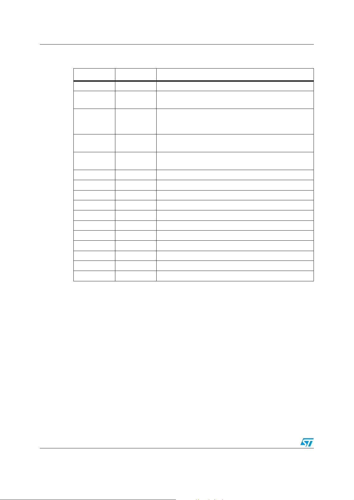
(TOP VIEW)
DIRECTIONS OF THE
DETECTABLE
ANGULAR RATE
1
X
Vdd_IO
SCL/SPC
SDA/SDI/SDO
SDO/SA0
RES
INT1
DRDY/INT2
CS
DEN
Cap
RES
Vdd
1
8
6
16
+ Ω
Z
+ Ω
X
BOTTOM
VIEW
+ Ω
Y
5
13
9
RES
RES
GND
GND
14
AM12690V1
1 Block diagram and pin description
Figure 1. Block diagram
The vibration of the structure is maintained by a drive circuitry in a feedback loop. The
sensing signal is filtered and appears as digital signal at the output.
1.1 Pin description
Figure 2. Pin connection
Doc ID 023469 Rev 1 5/25
Block diagram and pin description L3GD20H
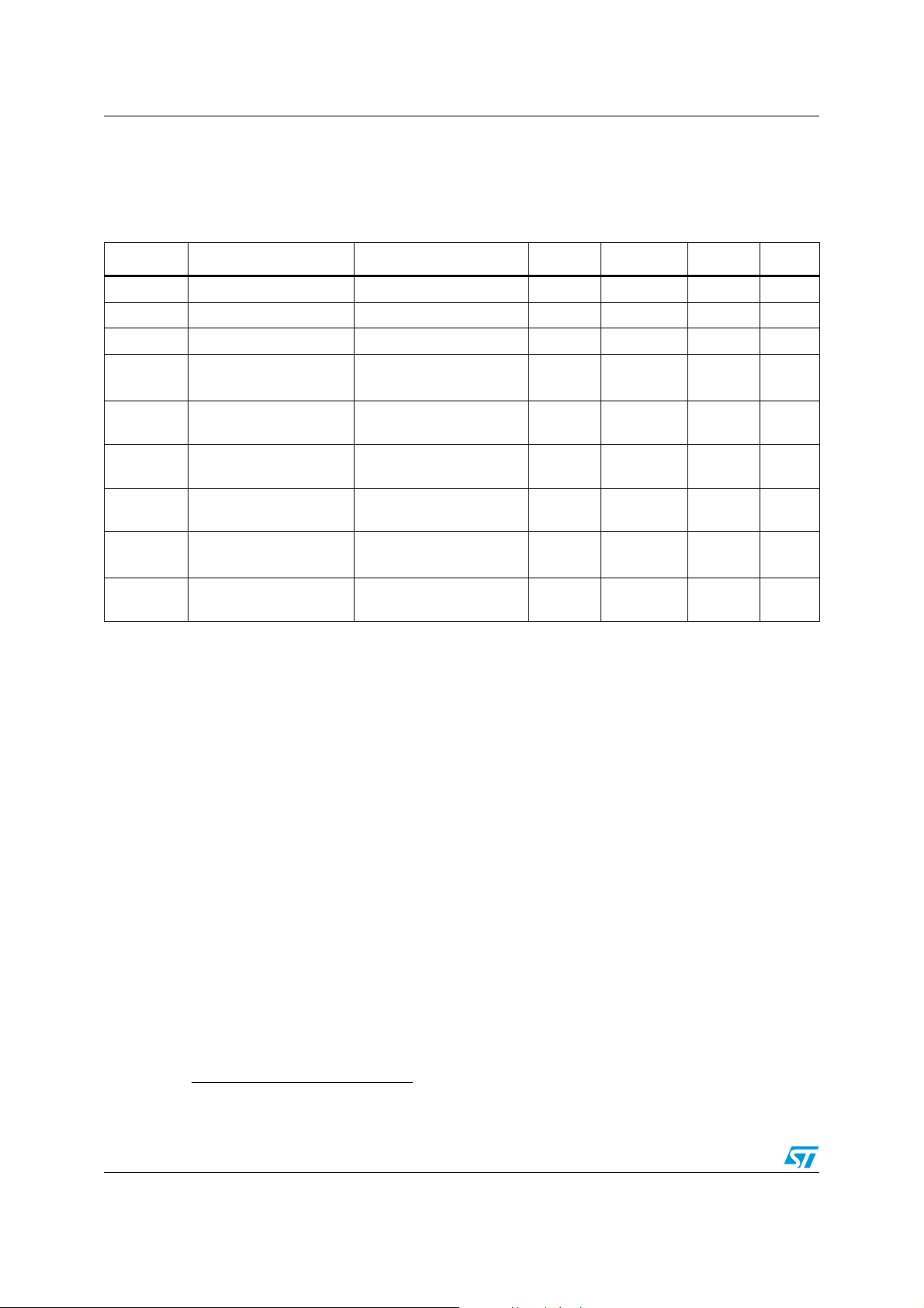
Table 2. Pin description
Pin# Name Function
(1)
1 Vdd_IO
2
SCL
SPC
SDA
3
SDI
SDO
Power supply for I/O pins
2
I
C serial clock (SCL)
SPI serial port clock (SPC)
2
I
C serial data (SDA)
SPI serial data input (SDI)
3-wire interface serial data output (SDO)
4
SDO
SA0
5CS
SPI serial data output (SDO)
2
I
C less significant bit of the device address (SA0)
SPI enable
2
I
C/SPI mode selection (1: I2C mode; 0: SPI enabled)
6 DRDY/INT2 Data ready/fifo interrupt (FIFO Threshold/overrun/empty)
7 INT1 Programmable Interrupt
8 DEN Gyroscope data enable
9 Reserved Connect to GND
10 Reserved Connect to GND
11 Reserved Connect to GND
12 GND 0 V supply
13 GND 0 V supply
14 Cap Connect to GND with ceramic capacitor
(2)
15 Reserved Connect to Vdd
16 Vdd
1. Recommended 100 nF filter capacitor.
2. 10 nF (+/-10%), 25 V. 1 nF minimum value has to be guaranteed under 12 V bias condition.
3. Recommended 100 nF plus 10 μF capacitors.
(3)
Power supply
6/25 Doc ID 023469 Rev 1
L3GD20H Mechanical and electrical specifications
dps/ Hz()
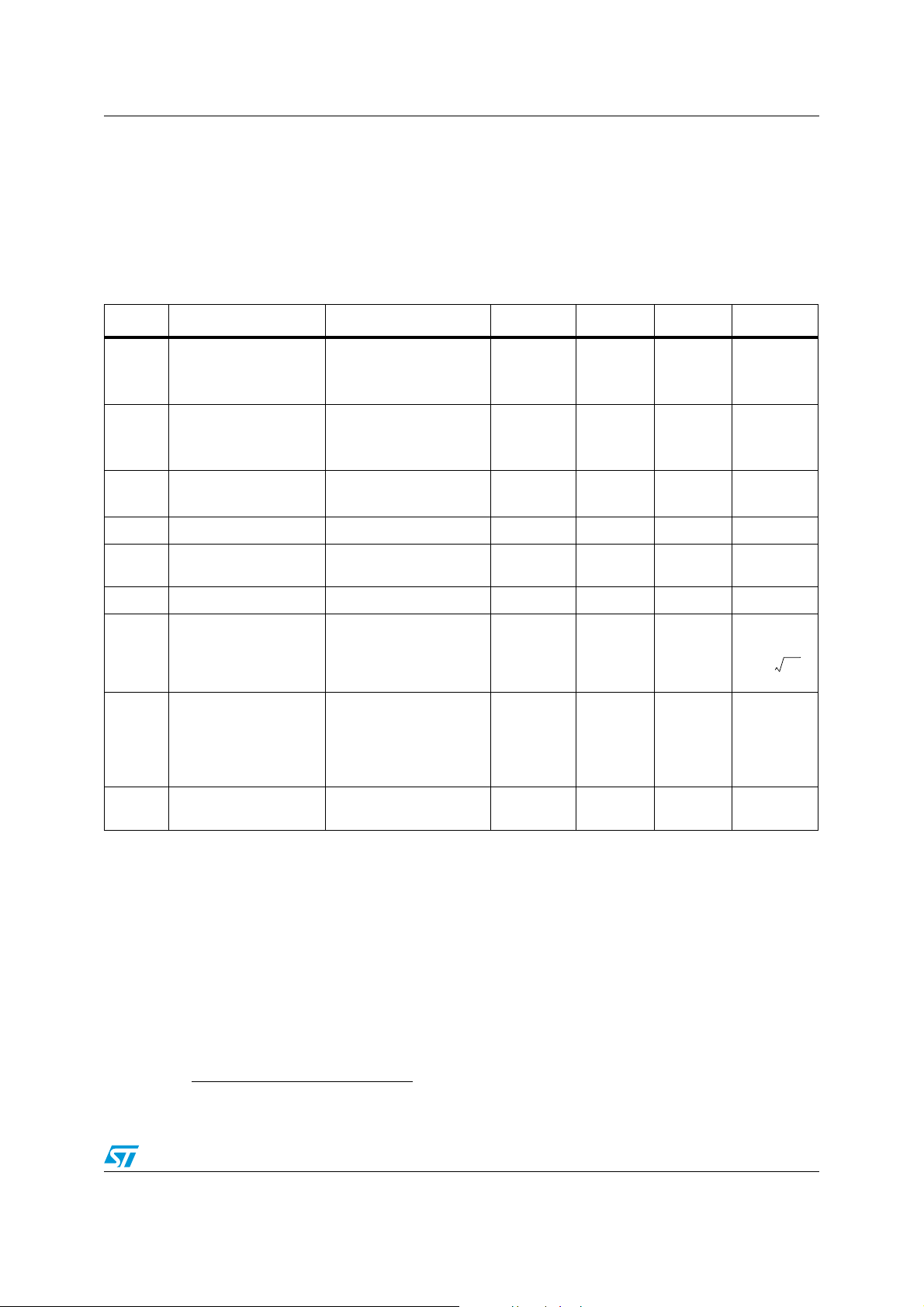
2 Mechanical and electrical specifications
2.1 Mechanical characteristics
@ Vdd = 3.0 V, T = 25 °C unless otherwise noted
Table 3. Mechanical characteristics
Symbol Parameter Test condition Min. Typ.
FS Measurement range User selectable
So Sensitivity
(a)
(1)
±245
±500
±2000
8.75
17.50
70.00
Max. Unit
dps
mdps/digit
SoDr
Sensitivity change vs.
temperature
(2)
From -40 °C to +85 °C
Delta from T = 25 °C
±2 %
DVoff Digital Zero-rate level FS = 2000 dps ±25 dps
OffDr
Zero-rate level change
vs temperature
NL Non linearity
(3)
(3)
Rn Rate noise density
FS = 2000 dps ±0.04 dps/°C
Best fit straight line 0.2 % FS
(3)
BW = 50 Hz 0.011
11.9/23.7/
47.3/94.7/
189.4/
378.8/
Hz
ODR
Digital output data
(3)
rate
757.6
Top
1. Typical specifications are not guaranteed.
2. Guaranteed by design.
3. The period (1/ODR), length of time between two consecutive sampling, must be derived by the reciprocal of the maximum.
and minimum ODR limits: for example for ODR = 189.4 Hz, sampling period range will be within [4591 μs, 6211 μs] (where
ODR minimum and maximum have been approximated at 162 Hz, 219 Hz respectively).
Operating temperature
range
-40 +85 °C
a. The product is factory calibrated at 3.0 V. The operational power supply range is specified in Table 4.
Doc ID 023469 Rev 1 7/25
Mechanical and electrical specifications L3GD20H
2.2 Electrical characteristics
@ Vdd =3.0 V, T=25 °C unless otherwise noted
Table 4. Electrical characteristics
Symbol Parameter Test condition Min. Typ.
Vdd Supply voltage 2.2 3.0 3.6 V
Vdd_IO I/O pins supply voltage
Idd Supply current 5.0 mA
(2)
(b)
(1)
Max. Unit
1.71 Vdd+0.1 V
IddSL
IddPdn
VIH
VIL
Ton Turn-on time
To p
1. Typical specifications are not guaranteed.
2. It is possible to remove Vdd maintaining Vdd_IO without blocking the communication busses, in this condition the
measurement chain is powered off.
3. Sleep mode introduces a faster turn-on time related to power down mode.
4. Time to obtain stable Sensitivity (within
Supply current
in sleep mode
(3)
Supply current in powerdown mode
Digital high level input
voltage
Digital low level input
voltage
(4)
Operating temperature
range
Selectable by digital
interface
Selectable by digital
interface
2.5 mA
1 μA
0.8*Vdd_I
O
0.2*Vdd_I
O
LPF2 disabled
ODR = 190 Hz
50 ms
-40 +85 °C
±5% of final value) after exiting power-down mode. It is guaranteed by design.
V
V
b. The product is factory calibrated at 3.0 V.
8/25 Doc ID 023469 Rev 1
 Loading...