

Features
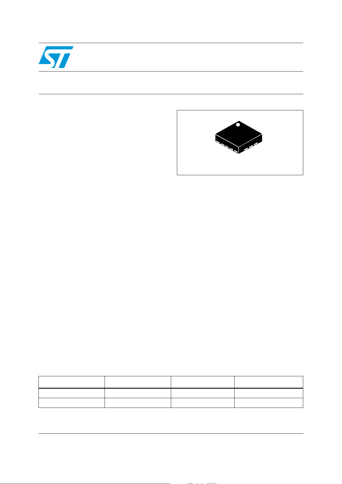
LGA-16
(3x3.5x1 mm)
■ Wide supply voltage, 2.4 V to 3.6 V
■ Wide extended operating temperature (-40 °C
to 85 °C)
■ Low voltage compatible IOs, 1.8 V
■ Low power consumption
■ Embedded power-down
■ Sleep mode
■ Three selectable fullscale
■ 16-bit rate value data output
■ 8-bit temperature data output
2
■ I
C/SPI digital output interface
■ Two dedicated lines (1 interrupt, 1 data ready)
■ User selectable bandwidth integrated low-pass
filters
■ User enable integrated high-pass filters
■ Embedded self-test
■ Embedded temperature sensor
■ Embedded FIFO
■ High shock survivability
■ ECOPACK
®
RoHS and “Green” compliant
L3G3200D
MEMS motion sensor:
three-axis digital output gyroscope
Preliminary data
Description
The L3G3200D is a low-power three-axis angular
rate sensor.
It includes a sensing element and an IC interface
able to provide the measured angular rate to the
external world through a digital interface
2
(I
C/SPI).
The sensing element is manufactured using a
dedicated micromachining process developed by
ST to produce inertial sensors and actuators on
silicon wafers. The IC interface is manufactured
using a CMOS process that allows a high level of
integration to design a dedicated circuit which is
trimmed to better match the sensing element
characteristics.
Applications
■ Gaming and virtual reality input devices
■ Motion control with MMI (man-machine
interface)
■ GPS navigation systems
■ Appliances and robotics
±2000 dps and is capable of measuring rates with
a user selectable bandwidth.
The L3G3200D is available in a plastic land grid
array (LGA) package and can operate within a
temperature range of -40 °C to +85 °C.
Table 1. Device summary
Order code Temperature range (°C) Package Packing
L3G3200D -40 to +85 LGA-16 (3x3.5x1.0) Tray
L3G3200DTR -40 to +85 LGA-16 (3x3.5x1.0) Tape and reel
December 2011 Doc ID 022557 Rev 1 1/45
The L3G3200D has a full scale of ±250/±500/
This is preliminary information on a new product now in development or undergoing evaluation. Details are subject to
change without notice.
www.st.com
45

Contents L3G3200D
Contents
1 Block diagram and pin description . . . . . . . . . . . . . . . . . . . . . . . . . . . . . 6
1.1 Pin description . . . . . . . . . . . . . . . . . . . . . . . . . . . . . . . . . . . . . . . . . . . . . . 6
2 Mechanical and electrical specifications . . . . . . . . . . . . . . . . . . . . . . . . 8
2.1 Mechanical characteristics . . . . . . . . . . . . . . . . . . . . . . . . . . . . . . . . . . . . . 8
2.2 Electrical characteristics . . . . . . . . . . . . . . . . . . . . . . . . . . . . . . . . . . . . . . . 9
2.3 Temperature sensor characteristics . . . . . . . . . . . . . . . . . . . . . . . . . . . . . . 9
2.4 Communication interface characteristics . . . . . . . . . . . . . . . . . . . . . . . . . 10
2.4.1 SPI - serial peripheral interface . . . . . . . . . . . . . . . . . . . . . . . . . . . . . . . 10
2.4.2 I2C - Inter IC control interface . . . . . . . . . . . . . . . . . . . . . . . . . . . . . . . . 11
2.5 Absolute maximum ratings . . . . . . . . . . . . . . . . . . . . . . . . . . . . . . . . . . . . 12
2.6 Terminology . . . . . . . . . . . . . . . . . . . . . . . . . . . . . . . . . . . . . . . . . . . . . . . 13
2.6.1 Sensitivity . . . . . . . . . . . . . . . . . . . . . . . . . . . . . . . . . . . . . . . . . . . . . . . . 13
2.6.2 Zero-rate level . . . . . . . . . . . . . . . . . . . . . . . . . . . . . . . . . . . . . . . . . . . . 13
2.7 Soldering information . . . . . . . . . . . . . . . . . . . . . . . . . . . . . . . . . . . . . . . . 13
3 Application hints . . . . . . . . . . . . . . . . . . . . . . . . . . . . . . . . . . . . . . . . . . . 14
4 Digital main blocks . . . . . . . . . . . . . . . . . . . . . . . . . . . . . . . . . . . . . . . . . 15
4.1 Block diagram . . . . . . . . . . . . . . . . . . . . . . . . . . . . . . . . . . . . . . . . . . . . . . 15
4.2 FIFO . . . . . . . . . . . . . . . . . . . . . . . . . . . . . . . . . . . . . . . . . . . . . . . . . . . . . 15
4.2.1 Bypass mode . . . . . . . . . . . . . . . . . . . . . . . . . . . . . . . . . . . . . . . . . . . . . 16
4.2.2 FIFO mode . . . . . . . . . . . . . . . . . . . . . . . . . . . . . . . . . . . . . . . . . . . . . . . 16
4.2.3 Stream mode . . . . . . . . . . . . . . . . . . . . . . . . . . . . . . . . . . . . . . . . . . . . . 17
4.2.4 Bypass-to-stream mode . . . . . . . . . . . . . . . . . . . . . . . . . . . . . . . . . . . . . 19
4.2.5 Stream-to-FIFO mode . . . . . . . . . . . . . . . . . . . . . . . . . . . . . . . . . . . . . . 19
4.2.6 Retrieve data from FIFO . . . . . . . . . . . . . . . . . . . . . . . . . . . . . . . . . . . . 20
5 Digital interfaces . . . . . . . . . . . . . . . . . . . . . . . . . . . . . . . . . . . . . . . . . . . 21
5.1 I2C serial interface . . . . . . . . . . . . . . . . . . . . . . . . . . . . . . . . . . . . . . . . . . 21
5.1.1 I2C operation . . . . . . . . . . . . . . . . . . . . . . . . . . . . . . . . . . . . . . . . . . . . . 22
5.2 SPI bus interface . . . . . . . . . . . . . . . . . . . . . . . . . . . . . . . . . . . . . . . . . . . 23
5.2.1 SPI read . . . . . . . . . . . . . . . . . . . . . . . . . . . . . . . . . . . . . . . . . . . . . . . . . 25
2/45 Doc ID 022557 Rev 1

L3G3200D Contents
5.2.2 SPI write . . . . . . . . . . . . . . . . . . . . . . . . . . . . . . . . . . . . . . . . . . . . . . . . 26
5.2.3 SPI read in 3-wire mode . . . . . . . . . . . . . . . . . . . . . . . . . . . . . . . . . . . . 26
6 Output register mapping . . . . . . . . . . . . . . . . . . . . . . . . . . . . . . . . . . . . 28
7 Register description . . . . . . . . . . . . . . . . . . . . . . . . . . . . . . . . . . . . . . . . 30
7.1 WHO_AM_I (0Fh) . . . . . . . . . . . . . . . . . . . . . . . . . . . . . . . . . . . . . . . . . . . 30
7.2 CTRL_REG1 (20h) . . . . . . . . . . . . . . . . . . . . . . . . . . . . . . . . . . . . . . . . . . 30
7.3 CTRL_REG2 (21h) . . . . . . . . . . . . . . . . . . . . . . . . . . . . . . . . . . . . . . . . . . 32
7.4 CTRL_REG3 (22h) . . . . . . . . . . . . . . . . . . . . . . . . . . . . . . . . . . . . . . . . . . 32
7.5 CTRL_REG4 (23h) . . . . . . . . . . . . . . . . . . . . . . . . . . . . . . . . . . . . . . . . . . 33
7.6 CTRL_REG5 (24h) . . . . . . . . . . . . . . . . . . . . . . . . . . . . . . . . . . . . . . . . . . 33
7.7 REFERENCE/DATACAPTURE (25h) . . . . . . . . . . . . . . . . . . . . . . . . . . . . 35
7.8 OUT_TEMP (26h) . . . . . . . . . . . . . . . . . . . . . . . . . . . . . . . . . . . . . . . . . . 35
7.9 STATUS_REG (27h) . . . . . . . . . . . . . . . . . . . . . . . . . . . . . . . . . . . . . . . . . 35
7.10 OUT_X_L (28h), OUT_X_H (29h) . . . . . . . . . . . . . . . . . . . . . . . . . . . . . . 36
7.11 OUT_Y_L (2Ah), OUT_Y_H (2Bh) . . . . . . . . . . . . . . . . . . . . . . . . . . . . . . 36
7.12 OUT_Z_L (2Ch), OUT_Z_H (2Dh) . . . . . . . . . . . . . . . . . . . . . . . . . . . . . . 36
7.13 FIFO_CTRL_REG (2Eh) . . . . . . . . . . . . . . . . . . . . . . . . . . . . . . . . . . . . . 36
7.14 FIFO_SRC_REG (2Fh) . . . . . . . . . . . . . . . . . . . . . . . . . . . . . . . . . . . . . . 37
7.15 INT1_CFG (30h) . . . . . . . . . . . . . . . . . . . . . . . . . . . . . . . . . . . . . . . . . . . . 37
7.16 INT1_SRC (31h) . . . . . . . . . . . . . . . . . . . . . . . . . . . . . . . . . . . . . . . . . . . . 38
7.17 INT1_THS_XH (32h) . . . . . . . . . . . . . . . . . . . . . . . . . . . . . . . . . . . . . . . . 38
7.18 INT1_THS_XL (33h) . . . . . . . . . . . . . . . . . . . . . . . . . . . . . . . . . . . . . . . . . 39
7.19 INT1_THS_YH (34h) . . . . . . . . . . . . . . . . . . . . . . . . . . . . . . . . . . . . . . . . 39
7.20 INT1_THS_YL (35h) . . . . . . . . . . . . . . . . . . . . . . . . . . . . . . . . . . . . . . . . . 39
7.21 INT1_THS_ZH (36h) . . . . . . . . . . . . . . . . . . . . . . . . . . . . . . . . . . . . . . . . 39
7.22 INT1_THS_ZL (37h) . . . . . . . . . . . . . . . . . . . . . . . . . . . . . . . . . . . . . . . . . 40
7.23 INT1_DURATION (38h) . . . . . . . . . . . . . . . . . . . . . . . . . . . . . . . . . . . . . . 40
8 Package information . . . . . . . . . . . . . . . . . . . . . . . . . . . . . . . . . . . . . . . . 42
9 Revision history . . . . . . . . . . . . . . . . . . . . . . . . . . . . . . . . . . . . . . . . . . . 43
Doc ID 022557 Rev 1 3/45

List of tables L3G3200D
List of tables
Table 3. Mechanical characteristics . . . . . . . . . . . . . . . . . . . . . . . . . . . . . . . . . . . . . . . . . . . . . . . . . . 7
Table 4. Electrical characteristics . . . . . . . . . . . . . . . . . . . . . . . . . . . . . . . . . . . . . . . . . . . . . . . . . . . . 8
Table 5. Electrical characteristics . . . . . . . . . . . . . . . . . . . . . . . . . . . . . . . . . . . . . . . . . . . . . . . . . . . . 8
Table 6. SPI slave timing values. . . . . . . . . . . . . . . . . . . . . . . . . . . . . . . . . . . . . . . . . . . . . . . . . . . . . 9
Table 7. I2C slave timing values . . . . . . . . . . . . . . . . . . . . . . . . . . . . . . . . . . . . . . . . . . . . . . . . . . . . 10
Table 8. Absolute maximum ratings . . . . . . . . . . . . . . . . . . . . . . . . . . . . . . . . . . . . . . . . . . . . . . . . . 11
Table 9. Serial interface pin description . . . . . . . . . . . . . . . . . . . . . . . . . . . . . . . . . . . . . . . . . . . . . . 20
Table 10. I2C terminology. . . . . . . . . . . . . . . . . . . . . . . . . . . . . . . . . . . . . . . . . . . . . . . . . . . . . . . . . . 20
Table 11. SAD+read/write patterns. . . . . . . . . . . . . . . . . . . . . . . . . . . . . . . . . . . . . . . . . . . . . . . . . . . 21
Table 12. Transfer when master is writing one byte to slave . . . . . . . . . . . . . . . . . . . . . . . . . . . . . . . 21
Table 13. Transfer when master is writing multiple bytes to slave . . . . . . . . . . . . . . . . . . . . . . . . . . . 22
Table 14. Transfer when master is receiving (reading) one byte of data from slave . . . . . . . . . . . . . 22
Table 15. Transfer when master is receiving (reading) multiple bytes of data from slave . . . . . . . . . 22
Table 16. Register address map. . . . . . . . . . . . . . . . . . . . . . . . . . . . . . . . . . . . . . . . . . . . . . . . . . . . . 27
Table 17. WHO_AM_I register . . . . . . . . . . . . . . . . . . . . . . . . . . . . . . . . . . . . . . . . . . . . . . . . . . . . . . 29
Table 18. CTRL_REG1 register . . . . . . . . . . . . . . . . . . . . . . . . . . . . . . . . . . . . . . . . . . . . . . . . . . . . . 29
Table 19. CTRL_REG1 description . . . . . . . . . . . . . . . . . . . . . . . . . . . . . . . . . . . . . . . . . . . . . . . . . . 29
Table 20. DR and BW configuration setting . . . . . . . . . . . . . . . . . . . . . . . . . . . . . . . . . . . . . . . . . . . . 30
Table 21. Power mode selection configuration. . . . . . . . . . . . . . . . . . . . . . . . . . . . . . . . . . . . . . . . . . 30
Table 22. CTRL_REG2 register . . . . . . . . . . . . . . . . . . . . . . . . . . . . . . . . . . . . . . . . . . . . . . . . . . . . . 31
Table 23. CTRL_REG2 description . . . . . . . . . . . . . . . . . . . . . . . . . . . . . . . . . . . . . . . . . . . . . . . . . . 31
Table 24. High-pass filter mode configuration . . . . . . . . . . . . . . . . . . . . . . . . . . . . . . . . . . . . . . . . . . 31
Table 25. High-pass filter cut-off frequency configuration [Hz] . . . . . . . . . . . . . . . . . . . . . . . . . . . . . . 31
Table 26. CTRL_REG1 register . . . . . . . . . . . . . . . . . . . . . . . . . . . . . . . . . . . . . . . . . . . . . . . . . . . . . 31
Table 27. CTRL_REG3 description . . . . . . . . . . . . . . . . . . . . . . . . . . . . . . . . . . . . . . . . . . . . . . . . . . 32
Table 28. CTRL_REG4 register . . . . . . . . . . . . . . . . . . . . . . . . . . . . . . . . . . . . . . . . . . . . . . . . . . . . . 32
Table 29. CTRL_REG4 description . . . . . . . . . . . . . . . . . . . . . . . . . . . . . . . . . . . . . . . . . . . . . . . . . . 32
Table 30. CTRL_REG5 register . . . . . . . . . . . . . . . . . . . . . . . . . . . . . . . . . . . . . . . . . . . . . . . . . . . . . 32
Table 31. CTRL_REG5 description . . . . . . . . . . . . . . . . . . . . . . . . . . . . . . . . . . . . . . . . . . . . . . . . . . 32
Table 32. Out_Sel configuration setting . . . . . . . . . . . . . . . . . . . . . . . . . . . . . . . . . . . . . . . . . . . . . . . 33
Table 33. INT_SEL configuration setting . . . . . . . . . . . . . . . . . . . . . . . . . . . . . . . . . . . . . . . . . . . . . . 33
Table 34. REFERENCE register. . . . . . . . . . . . . . . . . . . . . . . . . . . . . . . . . . . . . . . . . . . . . . . . . . . . . 34
Table 35. REFERENCE register description . . . . . . . . . . . . . . . . . . . . . . . . . . . . . . . . . . . . . . . . . . . 34
Table 36. OUT_TEMP register . . . . . . . . . . . . . . . . . . . . . . . . . . . . . . . . . . . . . . . . . . . . . . . . . . . . . . 34
Table 37. OUT_TEMP register description . . . . . . . . . . . . . . . . . . . . . . . . . . . . . . . . . . . . . . . . . . . . . 34
Table 38. STATUS_REG register . . . . . . . . . . . . . . . . . . . . . . . . . . . . . . . . . . . . . . . . . . . . . . . . . . . . 34
Table 39. STATUS_REG description . . . . . . . . . . . . . . . . . . . . . . . . . . . . . . . . . . . . . . . . . . . . . . . . . 34
Table 40. REFERENCE register. . . . . . . . . . . . . . . . . . . . . . . . . . . . . . . . . . . . . . . . . . . . . . . . . . . . . 35
Table 41. REFERENCE register description . . . . . . . . . . . . . . . . . . . . . . . . . . . . . . . . . . . . . . . . . . . 35
Table 42. FIFO mode configuration . . . . . . . . . . . . . . . . . . . . . . . . . . . . . . . . . . . . . . . . . . . . . . . . . . 35
Table 43. FIFO_SRC register . . . . . . . . . . . . . . . . . . . . . . . . . . . . . . . . . . . . . . . . . . . . . . . . . . . . . . . 36
Table 44. FIFO_SRC register description. . . . . . . . . . . . . . . . . . . . . . . . . . . . . . . . . . . . . . . . . . . . . . 36
Table 45. INT1_CFG register . . . . . . . . . . . . . . . . . . . . . . . . . . . . . . . . . . . . . . . . . . . . . . . . . . . . . . . 36
Table 46. INT1_CFG description . . . . . . . . . . . . . . . . . . . . . . . . . . . . . . . . . . . . . . . . . . . . . . . . . . . . 36
Table 47. INT1_SRC register . . . . . . . . . . . . . . . . . . . . . . . . . . . . . . . . . . . . . . . . . . . . . . . . . . . . . . . 37
Table 48. INT1_SRC description . . . . . . . . . . . . . . . . . . . . . . . . . . . . . . . . . . . . . . . . . . . . . . . . . . . . 37
Table 49. INT1_THS_XH register . . . . . . . . . . . . . . . . . . . . . . . . . . . . . . . . . . . . . . . . . . . . . . . . . . . . 37
Table 50. INT1_THS_XH description . . . . . . . . . . . . . . . . . . . . . . . . . . . . . . . . . . . . . . . . . . . . . . . . . 38
4/45 Doc ID 022557 Rev 1

L3G3200D List of tables
Table 51. INT1_THS_XL register . . . . . . . . . . . . . . . . . . . . . . . . . . . . . . . . . . . . . . . . . . . . . . . . . . . . 38
Table 52. INT1_THS_XL description . . . . . . . . . . . . . . . . . . . . . . . . . . . . . . . . . . . . . . . . . . . . . . . . . 38
Table 53. INT1_THS_YH register . . . . . . . . . . . . . . . . . . . . . . . . . . . . . . . . . . . . . . . . . . . . . . . . . . . . 38
Table 54. INT1_THS_YH description . . . . . . . . . . . . . . . . . . . . . . . . . . . . . . . . . . . . . . . . . . . . . . . . . 38
Table 55. INT1_THS_YL register . . . . . . . . . . . . . . . . . . . . . . . . . . . . . . . . . . . . . . . . . . . . . . . . . . . . 38
Table 56. INT1_THS_YL description . . . . . . . . . . . . . . . . . . . . . . . . . . . . . . . . . . . . . . . . . . . . . . . . . 38
Table 57. INT1_THS_ZH register . . . . . . . . . . . . . . . . . . . . . . . . . . . . . . . . . . . . . . . . . . . . . . . . . . . . 38
Table 58. INT1_THS_ZH description . . . . . . . . . . . . . . . . . . . . . . . . . . . . . . . . . . . . . . . . . . . . . . . . . 38
Table 59. INT1_THS_ZL register . . . . . . . . . . . . . . . . . . . . . . . . . . . . . . . . . . . . . . . . . . . . . . . . . . . . 39
Table 60. INT1_THS_ZL description . . . . . . . . . . . . . . . . . . . . . . . . . . . . . . . . . . . . . . . . . . . . . . . . . 39
Table 61. INT1_DURATION register . . . . . . . . . . . . . . . . . . . . . . . . . . . . . . . . . . . . . . . . . . . . . . . . . 39
Table 62. INT1_DURATION description . . . . . . . . . . . . . . . . . . . . . . . . . . . . . . . . . . . . . . . . . . . . . . . 39
Table 63. Document revision history . . . . . . . . . . . . . . . . . . . . . . . . . . . . . . . . . . . . . . . . . . . . . . . . . 42
Doc ID 022557 Rev 1 5/45

List of figures L3G3200D
List of figures
Figure 1. Block diagram . . . . . . . . . . . . . . . . . . . . . . . . . . . . . . . . . . . . . . . . . . . . . . . . . . . . . . . . . . . . 5
Figure 2. Pin connection . . . . . . . . . . . . . . . . . . . . . . . . . . . . . . . . . . . . . . . . . . . . . . . . . . . . . . . . . . . 5
Figure 3. SPI slave timing diagram . . . . . . . . . . . . . . . . . . . . . . . . . . . . . . . . . . . . . . . . . . . . . . . . . . . 9
Figure 4. I2C slave timing diagram . . . . . . . . . . . . . . . . . . . . . . . . . . . . . . . . . . . . . . . . . . . . . . . . . . 10
Figure 5. L3G3200D electrical connections and external component values . . . . . . . . . . . . . . . . . . 13
Figure 6. Block diagram . . . . . . . . . . . . . . . . . . . . . . . . . . . . . . . . . . . . . . . . . . . . . . . . . . . . . . . . . . . 14
Figure 7. Bypass mode . . . . . . . . . . . . . . . . . . . . . . . . . . . . . . . . . . . . . . . . . . . . . . . . . . . . . . . . . . . 15
Figure 8. FIFO mode . . . . . . . . . . . . . . . . . . . . . . . . . . . . . . . . . . . . . . . . . . . . . . . . . . . . . . . . . . . . . 16
Figure 9. Stream mode . . . . . . . . . . . . . . . . . . . . . . . . . . . . . . . . . . . . . . . . . . . . . . . . . . . . . . . . . . . 17
Figure 10. Bypass-to-stream mode . . . . . . . . . . . . . . . . . . . . . . . . . . . . . . . . . . . . . . . . . . . . . . . . . . . 18
Figure 11. Trigger Stream mode . . . . . . . . . . . . . . . . . . . . . . . . . . . . . . . . . . . . . . . . . . . . . . . . . . . . . 18
Figure 12. Read and write protocol . . . . . . . . . . . . . . . . . . . . . . . . . . . . . . . . . . . . . . . . . . . . . . . . . . . 23
Figure 13. SPI read protocol . . . . . . . . . . . . . . . . . . . . . . . . . . . . . . . . . . . . . . . . . . . . . . . . . . . . . . . . 24
Figure 14. Multiple bytes SPI read protocol (2-byte example) . . . . . . . . . . . . . . . . . . . . . . . . . . . . . . . 24
Figure 15. SPI write protocol . . . . . . . . . . . . . . . . . . . . . . . . . . . . . . . . . . . . . . . . . . . . . . . . . . . . . . . . 25
Figure 16. Multiple bytes SPI write protocol (2-byte example). . . . . . . . . . . . . . . . . . . . . . . . . . . . . . . 25
Figure 17. SPI read protocol in 3-wire mode . . . . . . . . . . . . . . . . . . . . . . . . . . . . . . . . . . . . . . . . . . . . 26
Figure 18. INT1_Sel and Out_Sel configuration block diagram . . . . . . . . . . . . . . . . . . . . . . . . . . . . . . 33
Figure 19. Wait disabled . . . . . . . . . . . . . . . . . . . . . . . . . . . . . . . . . . . . . . . . . . . . . . . . . . . . . . . . . . . 40
Figure 20. Wait enabled . . . . . . . . . . . . . . . . . . . . . . . . . . . . . . . . . . . . . . . . . . . . . . . . . . . . . . . . . . . . 40
Figure 21. LGA-16: mechanical data and package dimensions . . . . . . . . . . . . . . . . . . . . . . . . . . . . . 41
6/45 Doc ID 022557 Rev 1
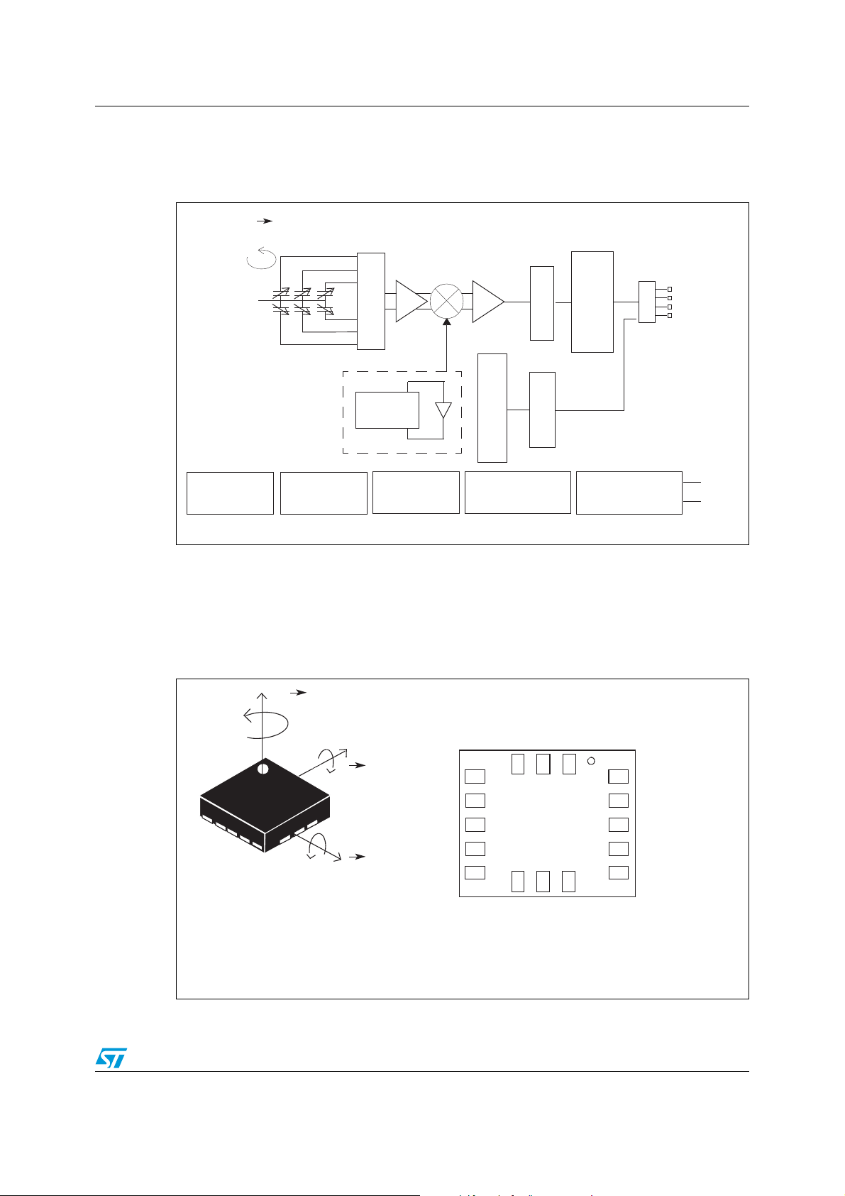
L3G3200D Block diagram and pin description
FIFO
TRIMMING
CIRCUITS
REFERENCE
MIXER
CHARGE
AMP
CLOCK
LOW-PASS
FILTER
+Ω
x,y,z
I2C
SPI
CS
SCL/SPC
SDA/SDO/SDI
SDO
Y+
Z+
Y-
Z-
X+
X-
DRIVING MASS
Feedback loop
M
U
X
A
D
D
C
I
G
I
T
A
L
F
I
L
T
E
R
I
N
G
CONTROL LOGIC
&
INTERRUPT GEN.
INT1
DRDY/INT2
A
D
C
T
E
M
P
E
R
A
T
U
R
E
S
E
N
S
O
R
1
2
&
PHASE GENERATOR
AM10190V1
1 Block diagram and pin description
Figure 1. Block diagram
The vibration of the structure is maintained by a drive circuitry in a feedback loop. The
sensing signal is filtered and appears as a digital signal at the output.
1.1 Pin description
Figure 2. Pin connection
(TOP VIEW)
DIRECTIONS OF THE
DETECTABLE
ANGULA RATES
+ Ω
RES
Z
X
+Ω
Y
GND
13
RES
14
RES
RES
RES
+Ω
X
RES
9
8
RES
Doc ID 022557 Rev 1 7/45
Vdd
16
BOTTOM
VIEW
6
INT1
DRDY/INT2
1
Vdd_IO
SCL/SPC
SDA/SDI/SDO
SDO/SA0
5
CS
AM10220V1
Block diagram and pin description L3G3200D
Table 2. Pin description
Pin# Name Function
SCL
SPC
SDA
SDI
SDO
SDO
SA0
(1)
Power supply for I/O pins
2
I
C serial clock (SCL)
SPI serial port clock (SPC)
2
C serial data (SDA)
I
SPI serial data input (SDI)
3-wire interface serial data output (SDO)
SPI serial data output (SDO)
2
C less significant bit of the device address (SA0)
I
2
C/SPI mode selection (1: SPI idle mode / I2C communication
I
enabled; 0: SPI communication mode / I2C disabled)
1 Vdd_IO
2
3
4
5CS
6 DRDY/INT2 Data Ready/FIFO Interrupt (Watermark/Overrun/Empty)
7 INT1 Programmable Interrupt
8 Reserved Connect to GND
9 Reserved Connect to GND
10 Reserved Connect to GND
11 Reserved Connect to GND
12 Reserved Connect to GND
13 GND 0 V supply
14 Reserved Connect to GND with ceramic capacitor
(2)
15 Reserved Connect to Vdd
16 Vdd
1. Recommended 100 nF filter capacitor.
2. 10 nF (+/-10%), 25 V. 1 nF minimum value has to be guaranteed under 11 V bias condition.
3. Recommended 100 nF plus 10 μF capacitors.
(3)
Power supply
8/45 Doc ID 022557 Rev 1
L3G3200D Mechanical and electrical specifications
dps Hz(⁄
2 Mechanical and electrical specifications
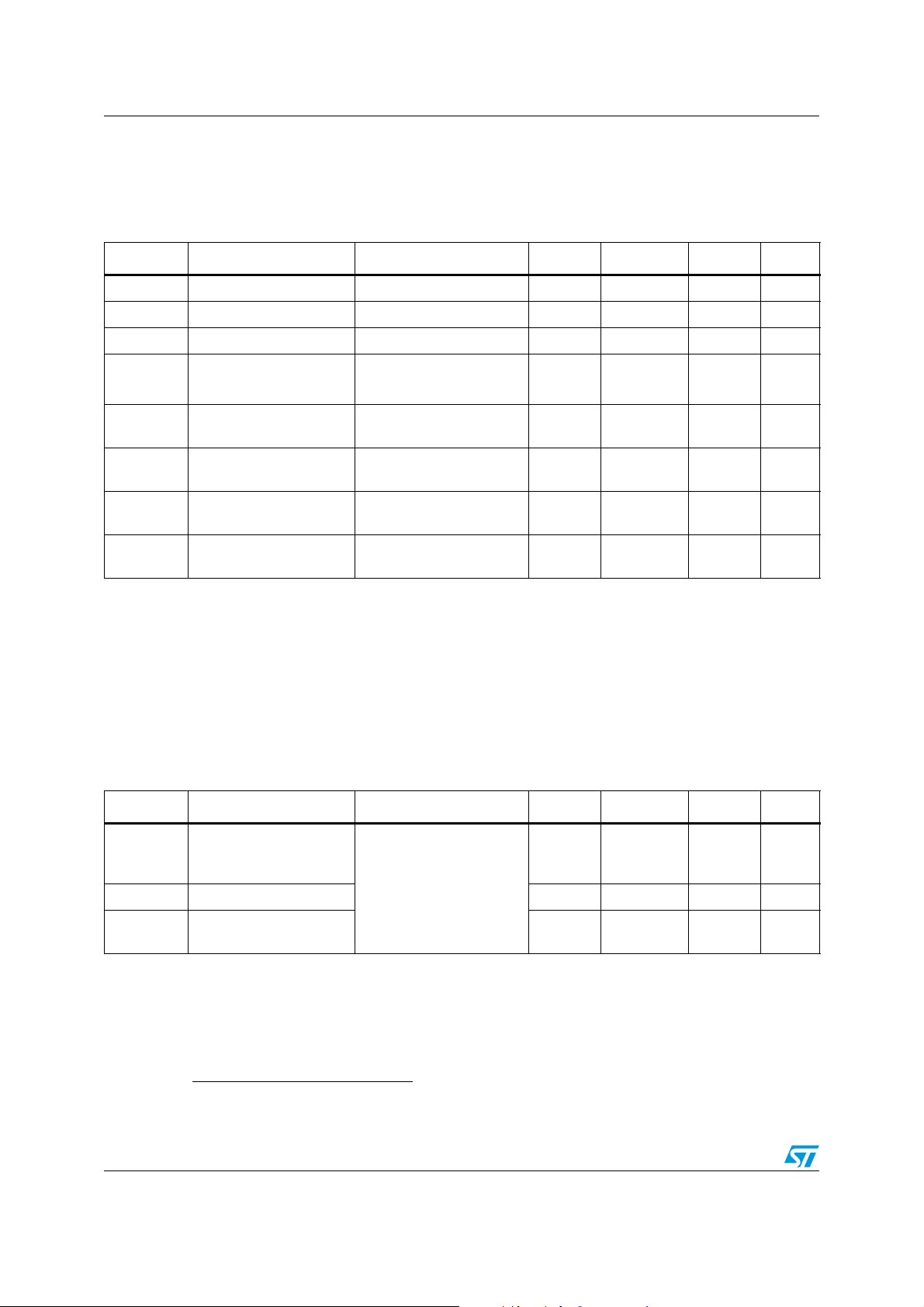
2.1 Mechanical characteristics
@ Vdd = 3.0 V, T = 25 °C unless otherwise noted
Table 3. Mechanical characteristics
Symbol Parameter Test condition Min. Typ.
FS Measurement range User selectable
So Sensitivity
SoDr
DVoff Digital Zero-rate level
OffDr
NL Non linearity
Rn Rate noise density
Sensitivity change vs.
temperature
Zero-rate level change
vs temperature
(2)
(2)
FS = 250 dps 8.75
FS = 2000 dps 70
From -40 °C to +85 °C ±2 %
FS = 250 dps ±10
FS = 2000 dps ±20
Best fit straight line 0.2 % FS
(a)
.
(1)
±250
±2000
±0.04 dps/°C
0.03
Max. Unit
dps±500
mdps/digitFS = 500 dps 17.50
dpsFS = 500 dps ±15
ODR Digital output data rate
Top
1. Typical specifications are not guaranteed.
2. Guaranteed by design.
Operating temperature
range
a. The product is factory calibrated at 3.0 V. The operational power supply range is specified in Table 4.
95/190/
380/760
Hz
-40 +85 °C
Doc ID 022557 Rev 1 9/45
Mechanical and electrical specifications L3G3200D
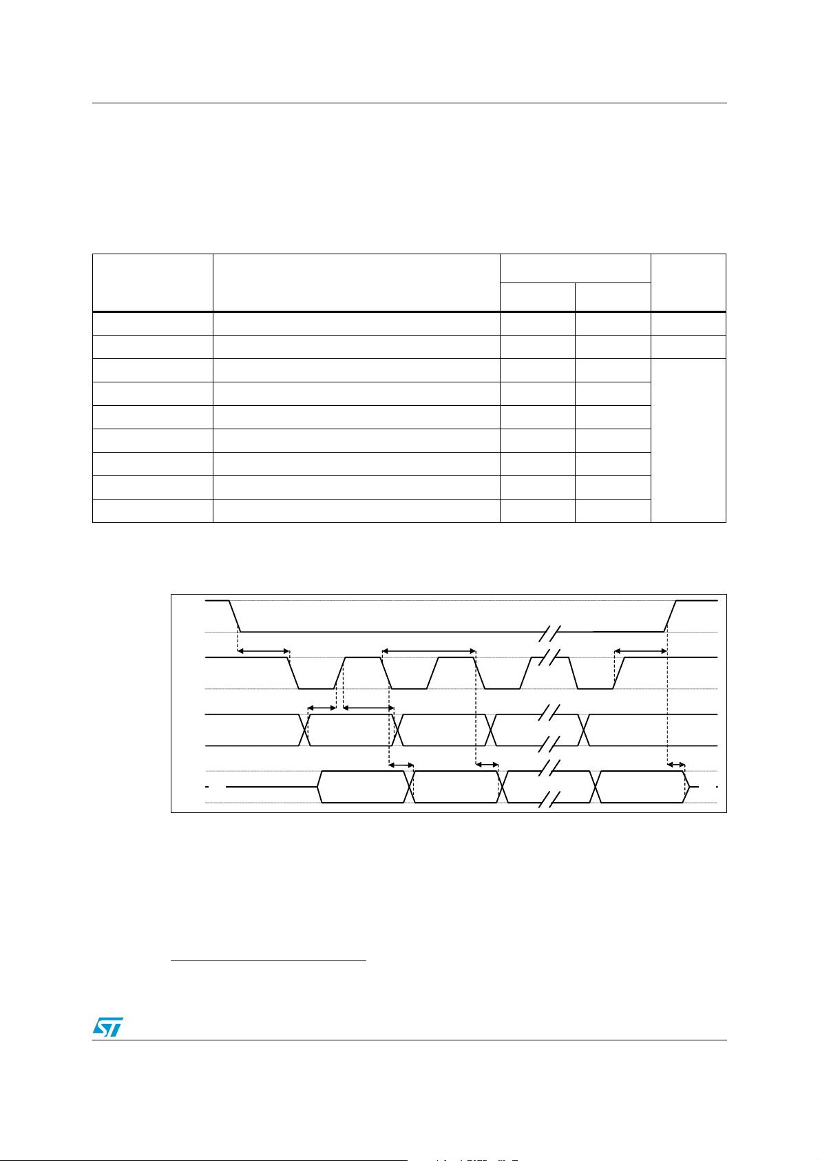
2.2 Electrical characteristics
@ Vdd = 3.0 V, T = 25 °C unless otherwise noted
Table 4. Electrical characteristics
Symbol Parameter Test condition Min. Typ.
Vdd Supply voltage 2.4 3.0 3.6 V
Vdd_IO I/O pins supply voltage
Idd Supply current 6.1 mA
(2)
(b)
.
(1)
1.71 Vdd+0.1 V
Max. Unit
IddSL
IddPdn
VIH
VIL
To p
1. Typical specifications are not guaranteed.
2. It is possible to remove Vdd maintaining Vdd_IO without blocking the communication busses, in this condition the
measurement chain is powered off.
3. Sleep mode introduce a faster turn-on time related to power down mode.
Supply current
in sleep mode
Supply current in powerdown mode
Digital high level input
voltage
Digital low level input
voltage
Operating temperature
range
(3)
Selectable by digital
interface
Selectable by digital
interface
2mA
5 μA
0.8*Vdd_I
O
0.2*Vdd_I
O
-40 +85 °C
2.3 Temperature sensor characteristics
@ Vdd = 3.0 V, T = 25 °C unless otherwise noted
Table 5. Electrical characteristics
Symbol Parameter Test condition Min. Typ.
(b)
.
(1)
Max. Unit
V
V
Temperature sensor
TSDr
TODR Temperature refresh rate 1 Hz
To p
1. Typical specifications are not guaranteed.
10/45 Doc ID 022557 Rev 1
output change vs.
temperature
Operating temperature
range
b. The product is factory calibrated at 3.0 V.
-1 °C/digit
-
-40 +85 °C
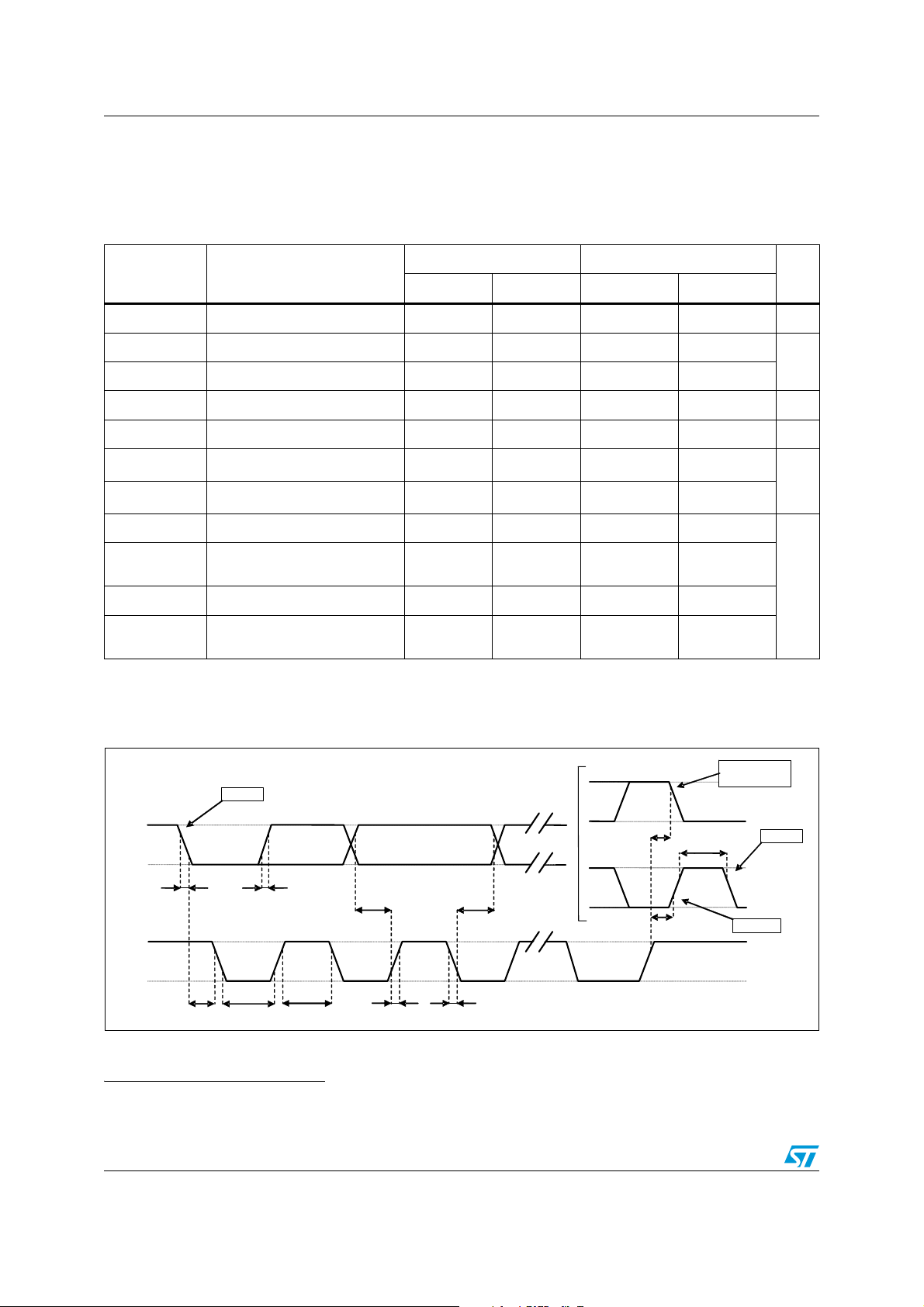
L3G3200D Mechanical and electrical specifications
SPC
CS
SDI
SDO
t
su(CS)
t
v(SO)
t
h(SO)
t
h(SI)
t
su(SI)
t
h(CS)
t
dis(SO)
t
c(SPC)
MSB IN
MSB OUT
LSB OUT
LSB IN
(3)
(3)
(3)
(3)
(3)
(3)
(3)
(3)
2.4 Communication interface characteristics
2.4.1 SPI - serial peripheral interface
Subject to general operating conditions for Vdd and Top.
Table 6. SPI slave timing values
(1)
Val ue
Symbol Parameter
Min. Max.
tc(SPC) SPI clock cycle 100 ns
fc(SPC) SPI clock frequency 10 MHz
tsu(CS) CS setup time 5
th(CS) CS hold time 20
tsu(SI) SDI input setup time 5
th(SI) SDI input hold time 15
tv(SO) SDO valid output time 50
th(SO) SDO output hold time 5
tdis(SO) SDO output disable time 50
Unit
ns
1. Values are guaranteed at 10 MHz clock frequency for SPI with both 4 and 3 wires, based on characterization results, not
tested in production.
(c)
Figure 3. SPI slave timing diagram
c. Measurement points are done at 0.2·Vdd_IO and 0.8·Vdd_IO, for both input and output ports.
Doc ID 022557 Rev 1 11/45
Mechanical and electrical specifications L3G3200D
SDA
SCL
t
f(SDA)
t
su(SP)
t
w(SCLL)
t
su(SDA)
t
r(SDA)
t
su(SR)
t
h(ST)
t
w(SCLH)
t
h(SDA)
t
r(SCL)
t
f(SCL)
t
w(SP:SR)
START
REPEATED
START
STOP
START
2.4.2 I2C - Inter IC control interface
Subject to general operating conditions for Vdd and Top.
Table 7. I2C slave timing values
Symbol Parameter
I2C standard mode
(1)
I2C fast mode
Min. Max. Min. Max.
(1)
Unit
f
(SCL)
t
w(SCLL)
t
w(SCLH)
t
su(SDA)
t
h(SDA)
t
r(SDA) tr(SCL)
t
f(SDA) tf(SCL)
t
h(ST)
t
su(SR)
t
su(SP)
t
w(SP:SR)
SCL clock frequency 100 400 kHz
SCL clock low time 4.7 1.3
SCL clock high time 4.0 0.6
SDA setup time 250 100 ns
SDA data hold time 0 3.45 0.01 0.9 µs
SDA and SCL rise time 1000
SDA and SCL fall time 300
START condition hold time 4 0.6
Repeated START condition
setup time
4.7 0.6
STOP condition setup time 4 0.6
Bus free time between STOP
and START condition
4.7 1.3
1. Data based on standard I2C protocol requirement, not tested in production.
2. Cb = total capacitance of one bus line, in pF.
Figure 4. I
2
C slave timing diagram
(d)
20 + 0.1C
20 + 0.1C
µs
(2)
b
(2)
b
300
ns
300
µs
d. Measurement points are done at 0.2·Vdd_IO and 0.8·Vdd_IO, for both ports.
12/45 Doc ID 022557 Rev 1
L3G3200D Mechanical and electrical specifications
This is a mechanical shock sensitive device, improper handling can cause permanent
damage to the part
This is an ESD sensitive device, improper handling can cause permanent damage to
the part
2.5 Absolute maximum ratings
Stresses above those listed as “Absolute maximum ratings” may cause permanent damage
to the device. This is a stress rating only and functional operation of the device under these
conditions is not implied. Exposure to maximum rating conditions for extended periods may
affect device reliability.
Table 8. Absolute maximum ratings
Symbol Ratings Maximum value Unit
Vdd Supply voltage -0.3 to 4.8 V
Vdd_IO I/O pins Supply voltage -0.3 to 4.8 V
Vin
T
ESD Electrostatic discharge protection 2 (HBM) kV
Note: Supply voltage on any pin should never exceed 4.8 V
Input voltage on any control pin (SCL, SDA, DEN,
CS)
Storage temperature range -40 to +125 °C
STG
-0.3 to Vdd_IO +0.3 V
Sg Acceleration g for 0.1 ms 10,000 g
Doc ID 022557 Rev 1 13/45

Mechanical and electrical specifications L3G3200D
2.6 Terminology
2.6.1 Sensitivity
An angular rate gyroscope is device that produces a positive-going digital output for
counterclockwise rotation around the sensible axis considered. Sensitivity describes the
gain of the sensor and can be determined by applying a defined angular velocity to it. This
value changes very little over temperature and time.
2.6.2 Zero-rate level
Zero-rate level describes the actual output signal if there is no angular rate present. Zerorate level of precise MEMS sensors is, to some extent, a result of stress to the sensor and
therefore zero-rate level can slightly change after mounting the sensor onto a printed circuit
board or after exposing it to extensive mechanical stress. This value changes very little over
temperature and time.
2.7 Soldering information
The LGA package is compliant with the ECOPACK®, RoHS and “Green” standard.
It is qualified for soldering heat resistance according to JEDEC J-STD-020.
Leave “Pin 1 Indicator” unconnected during soldering.
Land pattern and soldering recommendations are available at www.st.com/mems
.
14/45 Doc ID 022557 Rev 1
 Loading...