L296
®
HIGH CURRENT SWITCHING REGULAT ORS
4 A OUTP UT CURRENT
.
5.1 V TO 40 V OUTPUT VOLTAGE RANGE
.
0 TO 100 % DUTY CYCLE R A NG E
.
PRECISE (±2 %) ON-CHI P RE FE RE NCE
.
SWITCHING FREQUENCY UP TO 200 KHz
.
VERY HIGH EFFICIENCY (UP TO 90 %)
.
VERY FEW EXTERNAL COMPONENTS
.
SOFT START
.
RESET OUTP UT
.
EXTERNAL PROGRAMMABLE LIMITING
.
CURRENT (L296P)
CONTROL CIRCUIT FOR CROWBAR SCR
.
INPUT FOR REMOTE INHIBIT AND
.
SYNCHRONUS PWM
THERMAL SHUTDOWN
.
DESCRIPTION
The L296 and L296P are stepdo wn power s witching
regulators delivering 4 A at a voltage variable from
5.1 V to 40 V.
Features of the devices includ e soft start, rem ote in-
hibit, thermal protection, a reset output for microprocessors and a PWM comparator input for synchroniz ation in multichip c onf ig ur at ion s.
The L296P inc udes e xtern al prog rammab le lim iting
current.
L296P
Multiwatt
(15 lead )
ORDERING NUMBERS :
L296 (Vertical) L296HT (Horizontal)
L296P (Vertical) L296PHT (Horizontal)
The L296 a nd L296P are mo unted in a 15-lead Multiwatt plastic power package and requir es very few
external com po nents.
Efficient operation at switching frequencies up to
200 KHz allows a reduction in the size and cost of
external filter components. A voltage sense input
and SCR drive output are provided for optional
crowbar overvoltage protection with an external
SCR.
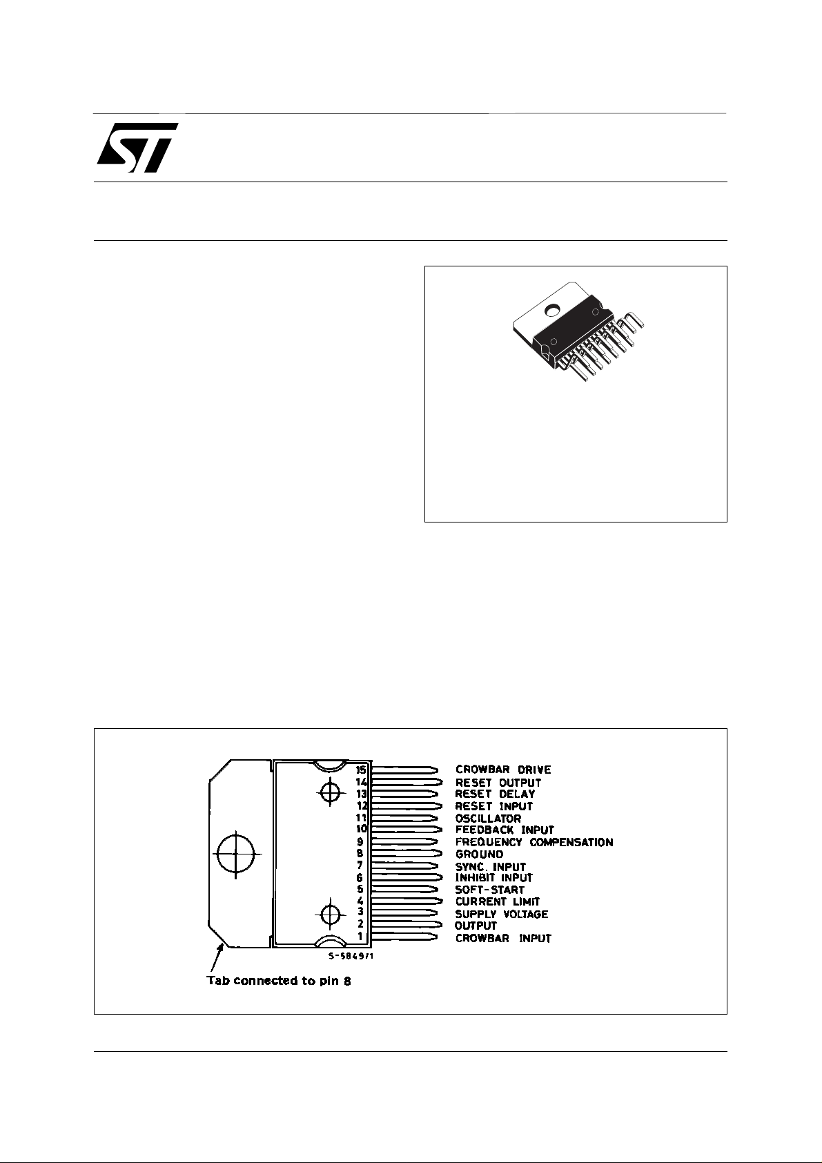
PIN CONNECTION (top view)
June 2000
1/22
L296 - L296P
PIN FUNCTIONS
N
°
1 CROWBAR INPUT Voltage Sense Input for Crowbar Overvoltage Protection. Normally connected to the
2 OUTPUT Regulator Output
3 SUPPLY VOLTAGE Unrergulated Voltage Input. An internal Regulator Powers the L296s Internal Logic.
4 CURRENT LIMIT A resistor connected between this terminal and ground sets the current limiter
5 SOFT START Soft Start Time Constant. A capacitor is connected between this terminal and ground
6 INHIBIT INPUT TTL – Level Remote Inhibit. A logic high level on this input disables the device.
7 SYNC INPUT Multiple L296s are synchronized by connecting the pin 7 inputs together and omitting
8 GROUND Common Ground Terminal
9 FREQUENCY
10 FEEDBACK INPUT The Feedback Terminal on the Regulation Loop. The output is connected directly to
11 OSCILLATOR A parallel RC networki connected to this terminal determines the switching frequency.
12 RESET INPUT Input of the Reset Circuit. The threshold is roughly 5 V. It may be connected to the
13 RESET DELAY A capacitor connected between this terminal and ground determines the reset signal
14 RESET OUTPUT Open collector reset signal output. This output is high when the supply is safe.
15 CROWBAR OUTPUT SCR gate drive output of the crowbar circuit.
Name Function
feedback input thus triggering the SCR when V
also monitor the input and a voltage divider can be added to increase the threshold.
Connected to ground when SCR not used.
threshold. If this terminal is left unconnected the threshold is internally set (see
electrical characteristics).
to define the soft start time constant. This capacitor also determines the average
short circuit output current.
the oscillator RC network on all but one device.
COMPENSATION
A series RC network connected between this terminal and ground determines the
regulation loop gain characteristics.
this terminal for 5.1V operation ; it is connected via a divider for higher voltages.
This pin must be connected to pin 7 input when the internal oscillator is used.
feedback point or via a divider to the input.
delay time.
exceeds nominal by 20 %. May
out
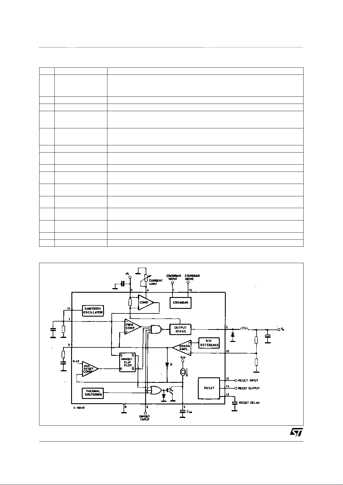
BLOCK DIAGRAM
2/22
L296 - L296P
CIRCUIT OPERATION
(refer to the block diagram)
The L296 and L296P are monolithic stepdown
switching regulators pr ov iding output v olt ag es f r om
5.1V to 40V and delivering 4A.
The regu lation loop consist s of a sawtooth osc illator,
error ampl ifier, compar ator and the outpu t stage. An
error signal is produced by comparing the output
voltage with a precise 5.1V on-c hip reference (ze ner
zap trimm ed to ± 2 %) . This e rror si gnal i s then compared wit h the sawtoot h signal to generate t he fixed
frequency pulse width mo dulated pulses w hich drive
the output stage. T he gain and frequ ency s tability of
the loop can be ad justed by an exter nal RC n etwork
connected to pin 9. Closing the loo p directly give s an
output voltag e of 5.1V. Higher voltage s are obtained
by inser ting a v oltage divider.
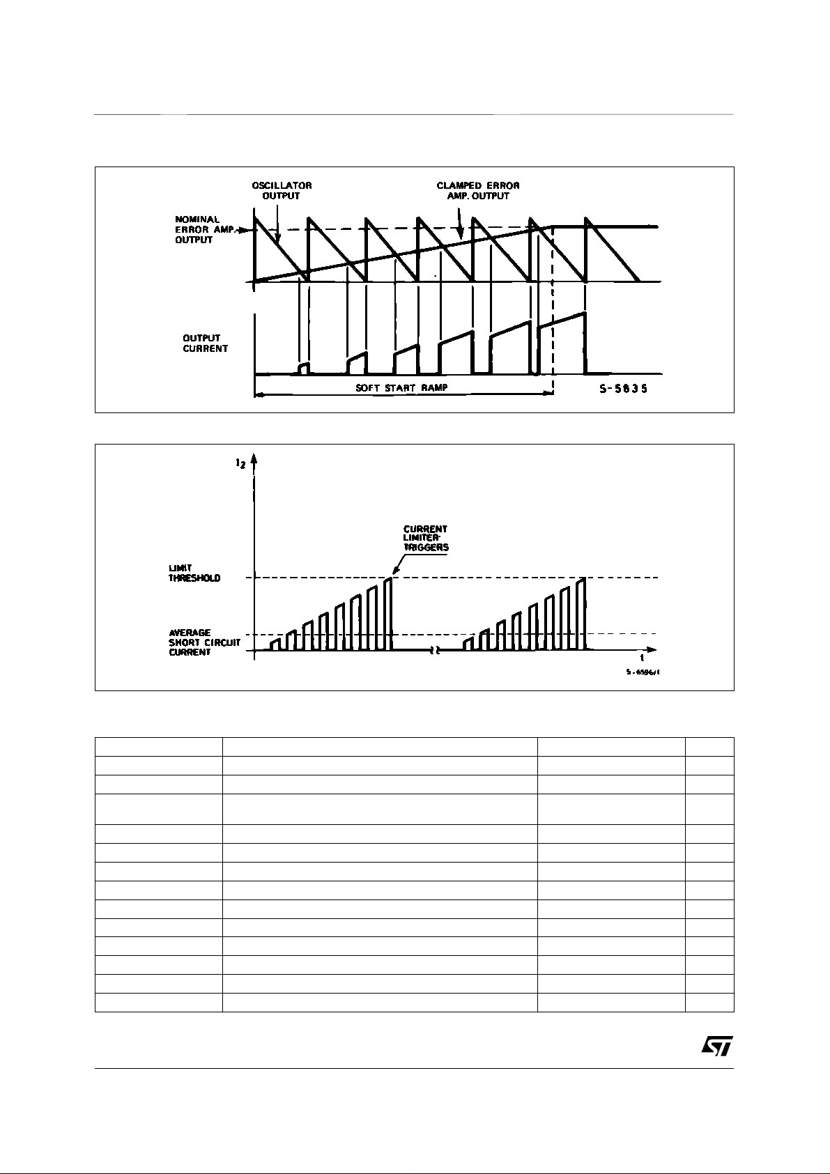
Output overcurrents at switch on are prevented by
the soft start function. The error amplifier output is
initially clamped by the external capacitor Css and
allowed to ris e, line arly , as t his capacit or i s char ged
by a constant current source.
Output over load protection is provided in the for m of
a current limiter. The load current is sensed by an
internal metal resistor connected to a comparator.
When the load current exceeds a preset threshold
this comparator sets a flip flop which disables the
output stage an d discharge s the soft start ca pacitor.
A second comparator resets the flip flop when the
voltage acro ss the so ft sta rt ca pacit or has f allen to
0.4V. The output stage is thus re-enabled and the
output voltage rises under control of the soft start
network. If the overload c ondit ion is still p rese nt the
limiter will trigger again when the threshold current
is reached. The average short circuit current is limited to a safe value by the dea d ti me intro duc ed by
the soft start net wo rk .
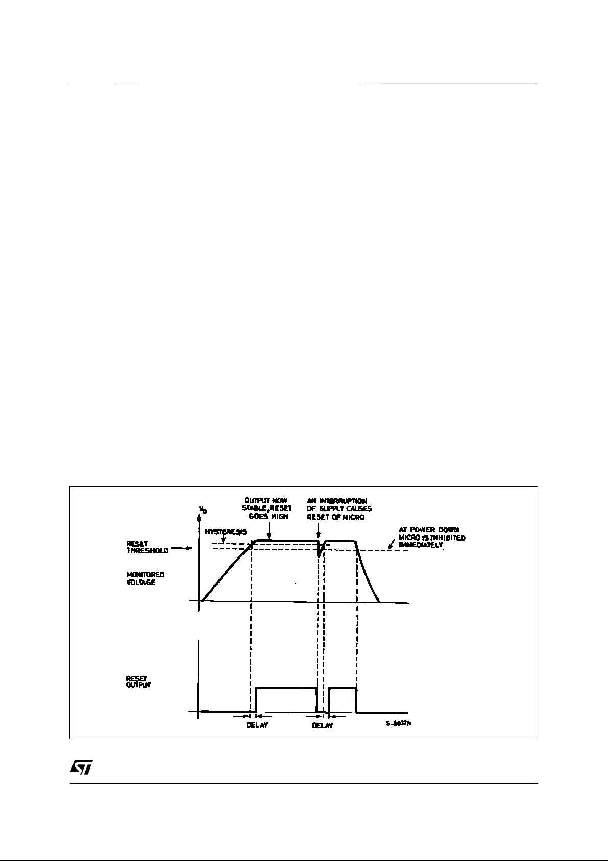
The reset circuit generates an output signal when
the supply voltage exceeds a threshold programmed by an exte rnal d ivide r. The re set si gnal is
generated wi th a delay time prog rammed by an ex ternal capacitor. When the supply falls below the
threshold the reset output goes low immediately.
The reset outp ut is an ope n co llector.
The scrowbar circui t senses the outp ut voltage an d
the crowbar out pu t c an pr ov ide a curren t of 1 00m A
to switch o n an externa l SCR. Thi s SCR is trigg ered
when the output voltage exceeds the nominal by
20%. There is no internal connection between the
output and cr owbar sense i npu t theref ore the crow bar can moni tor ei t her the input or the output.
A TTL - level inhibit i nput is provided for ap plicati ons
such as rem ote on/off control. This input is a ctivated
by high logic level a nd disab les circ uit operat ion. After an inhibit the L296 restarts under control of the
soft start network.
The thermal overload circuit disables circuit operation when the junction temperature reaches about
150 ° C and has hys teres is to pre vent un stable c on ditions.
Figure 1 : Reset Output Waveforms
3/22
L296 - L296P
Figure 2 : Soft Start Waveforms
Figure 3 : Cur r ent Lim iter Wavefor ms
ABSOLUTE MAXIMUM RATIN GS
Symbol Parameter Value Unit
V
i
V
– V
i
2
V
2
, V
V
1
12
V
15
, V5, V7, V9, V13Voltage at Pins 4, 5, 7, 9 and 13 5.5 V
V
4
, V
V
10
6
V
14
I
9
I
11
I
14
P
tot
, T
T
j
stg
4/22
Input Voltage (pin 3) 50 V
Input to Output Voltage Difference 50 V
Output DC Voltage
Output Peak Voltage at t = 0.1 µsec f = 200KHz
– 1
– 7
Voltage at Pins 1, 12 10 V
Voltage at Pin 15 15 V
Voltage at Pins 10 and 6 7 V
Voltage at Pin 14 (I14 ≤ 1 mA) V
i
Pin 9 Sink Current 1 mA
Pin 11 Source Current 20 mA
Pin 14 Sink Current (V14 < 5 V) 50 mA
Power Dissipation at T
≤ 90 °C20W
case
Junction and Storage Temperature – 40 to 150
V
V
C
°

L296 - L296P
THERMAL DATA
Symbol Parameter Value Unit
R
th j-case
R
th j-amb
ELECTRICAL CHARACTERISTICS
(refer to the test circuits T
Symbol Parameter Test Conditions Min. Typ. Max. Unit Fig.
DYNAMIC CHARACTERISTICS (pin 6 to GND unless otherwise specified)
V
o
V
i
V
i
V
∆
o
V
∆
o
V
ref
V
∆
ref
T
∆
V
d
I
2L
I
SH
η
SVR Supply Voltage Ripple Rejection
f Switching Frequency 85 100 115 kHz 4
f
∆
V
∆
i
f
∆
T
∆
j
f
max
T
sd
DC CHARACTERISTICS
I
3Q
– I
2L
Thermal Resistance Junction-case Max. 3
Thermal Resistance Junction-ambient Max. 35
= 25oC, Vi = 35V, unless otherwise specified)
j
Output Voltage Range Vi = 46V, Io = 1A V
Input Voltage Range Vo = V
Input Voltage Range Note (1), Vo = V
Line Regulation Vi =10V to 40V, Vo = V
Load Regulation Vo = V
to 36V, Io ≤ 3A 9 46V4
ref
to 36V Io = 4A 46 V 4
REF
, Io = 2A 15 50 mV 4
ref
ref
Io = 2A to 4A
ref
Io = 0.5A to 4A
40V4
101530
45
C/W
°
C/W
°
mV 4
Internal Reference Voltage (pin 10) Vi = 9V to 46V, Io = 2A 5 5.1 5.2 V 4
Average Temperature Coefficient
Tj = 0°C to 125°C, Io = 2A 0.4 mV/°C
of Reference Voltage
Dropout Voltage Between Pin 2
and Pin 3
Current Limiting Threshold (pin 2) L296 - Pin 4 Open,
Io = 4A
Io = 2A
Vi = 9V to 40V, Vo = V
L296P - V
= 9V to 40V, Vo = V
i
Pin 4 Open
R
= 22k
Iim
Ω
to 36V
ref
2
3.2
1.3
2.1
4.5 7.5 A 4
ref
5
2.5
7
4.5
V
V
A4
Input Average Current Vi = 46V, Output Short-circuited 60 100 mA 4
Efficiency I
Voltage Stability of Switching
= 3 A
o
∆
V
= 2 V
V
i
= V
o
Vo = V
ref
Vo = 12V
rms
, Io = 2A
ref
, f
ripple
= 100Hz
75
85
50 56 dB 4
Vi = 9V to 46V 0.5 % 4
%4
Frequency
Temperature Stability of Switching
Tj = 0°C to 125°C1%4
Frequency
Maximum Operating Switching
Frequency
Thermal Shutdown Junction
Vo = V
, Io = 1A 200 kHz –
ref
Note (2) 135 145
C–
°
Temperature
Quiescent Drain Current Vi = 46V, V7 = 0V, S1 : B, S2 : B
V6 = 0V
= 3V
V
6
Output Leakage Current Vi = 46V, V6 = 3V, S1 : B, S2 : A,
66
30
85
40
2mA
V7 = 0V
4
4
mA
Note
(1) : Using min. 7 A schottky dio de.
(2) : Guaranteed by desi gn, not 100 % test ed in pro duc tion.
5/22

L296 - L296P
ELECTRICAL CHARACTERISTICS (continued)
Symbol Parameter Test Conditions Min. Typ. Max. Unit Fig.
SOFT START
I
I
Source Current V6 = 0V, V5 = 3V 80 130 150
5 so
Sink Current V6 = 3V, V5 = 3V 50 70 120
5 si
INHIBIT
V
– I
– I
Input Voltage
V
6L
6H
Low Level
High Level
Input Current
with Input Voltage
6L
6H
Low Level
High Level
Vi = 9V to 46V, V7 = 0V,
S1 : B, S2 : B – 0.3
Vi = 9V to 46V, V7 = 0V,
S1 : B, S2 : B
ERROR AMPLIFIER
V
V
I
– I
High Level Output Voltage V10 = 4.7V, I9 = 100µA,
9H
Low Level Output Voltage V10 = 5.3V, I9 = 100µA,
9L
Sink Output Current V10 = 5.3V, S1 : A, S2 : B 100 150
9 si
Source Output Current V10 = 4.7V, S1 : A, S2 : D 100 150
9 so
Input Bias Current V10 = 5.2V, S1 : B
I
10
DC Open Loop Gain V9 = 1V to 3V, S1 : A, S2 : C 46 55 dB 6c
G
v
S1 : A, S2 : A
S1 : A, S2 : E
V
OSCILLATOR AND PWM COMPARATOR
– I
– I
Input Bias Current of
7
PWM Comparator
Oscillator Source Current V11 = 2V, S1 : A, S2 : B 5 mA
11
V7 = 0.5V to 3.5V 5
RESET
V
Rising Threshold Voltage
12 R
V
V
12 F
V
13 D
V
13 H
V
14 S
I
12
Falling Threshold Voltage 4.75 V
Delay Thershold Voltage
Delay Threshold Voltage
Hysteresis
Output Saturation Voltage I14 = 16mA, V12 = 4.7V, S1, S2 : B 0.4 V 6d
Input Bias Current V12 = 0V to V
S1 : B, S2 : B
V
V
– I
I
Delay Source Current
13 so
Delay Sink Current
13 si
I
Output Leakage Current Vi = 46V, V12 = 5.3V, S1 : B, S2 : A 100
14
CROWBAR
V
Input Threshold Voltage S1 : B 5.5 6 6.4 V 6b
1
V
– I
Output Saturation Voltage Vi = 9V to 46V, Vi = 5.4V,
15
I
Input Bias Current V1 = 6V, S1 : B 10
1
Output Source Current Vi = 9V to 46V, V1 = 6.5V,
15
I
V15 = 2V, S1 : B
= 0.8V
V
6
V6 = 2V
= 6.4V, S1 : B, L296P
10
= 9V to 46V,
i
= 5.3V, S1 : A, S2 : B
12
, S1 : B, S2 : B 1 3
ref
= 3V, S1 : A, S2 : B
13
= 5.3V
V
12
V12 = 4.7V
= 5mA, S1 : A
15
2
5.5
10
3
3.5 V 6c
0.5 V 6c
0.8
V
ref
-150mV
2
2
V
ref
-100mV
ref
-150mV
10
10
V
ref
-50mV
V
ref
-100mV
4.3 4.5 4.7 V 6d
100 mV 6d
70
110 140
10
0.2 0.4 V 6b
70 100 mA 6b
A6b
µ
A6b
µ
V6a
A6a
µ
A6c
µ
A6c
µ
A
µ
A6c6c
µ
A6a
µ
V6d
V6d
A6d
µ
A
µ
mA
A6d
µ
A6b
µ
6d
6/22
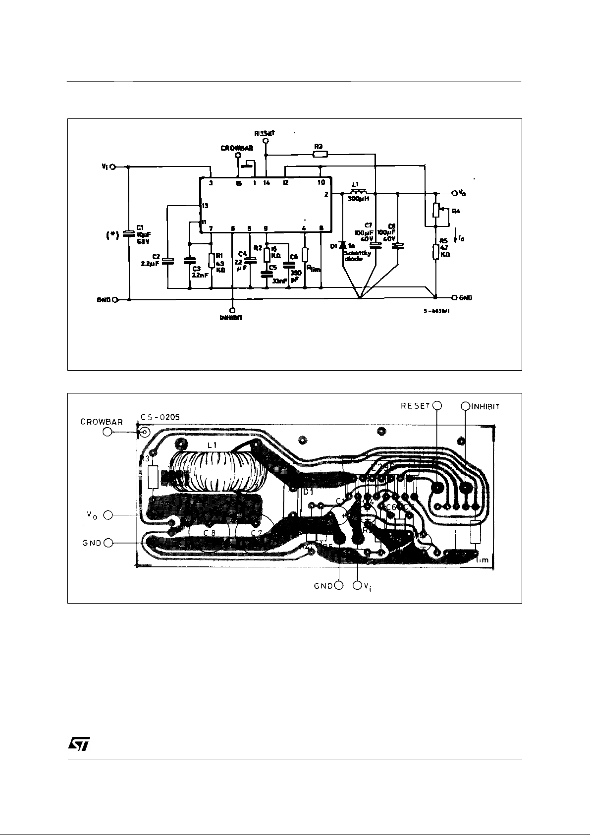
Figure 4 : Dynamic Test Circuit
C7, C8 : EKR (ROE)
L1 : L = 300 µH at 8 A Core type : MAGNETICS 58930 - A 2 MPP
N° turns : 43 Wire Gauge : 1 mm (18 A WG) COGEM A 9 46044
(*) Minimum suggested va lue (10 µF) to avoid oscillation s. Ri pple considera t ion leads to t ypical value of 1000 µF or higher.
L296 - L296P
Figure 5 : PC. Board and Component La yo ut of the Cir c uit of F ig ure 4 (1 :1 scale)
7/22
 Loading...