

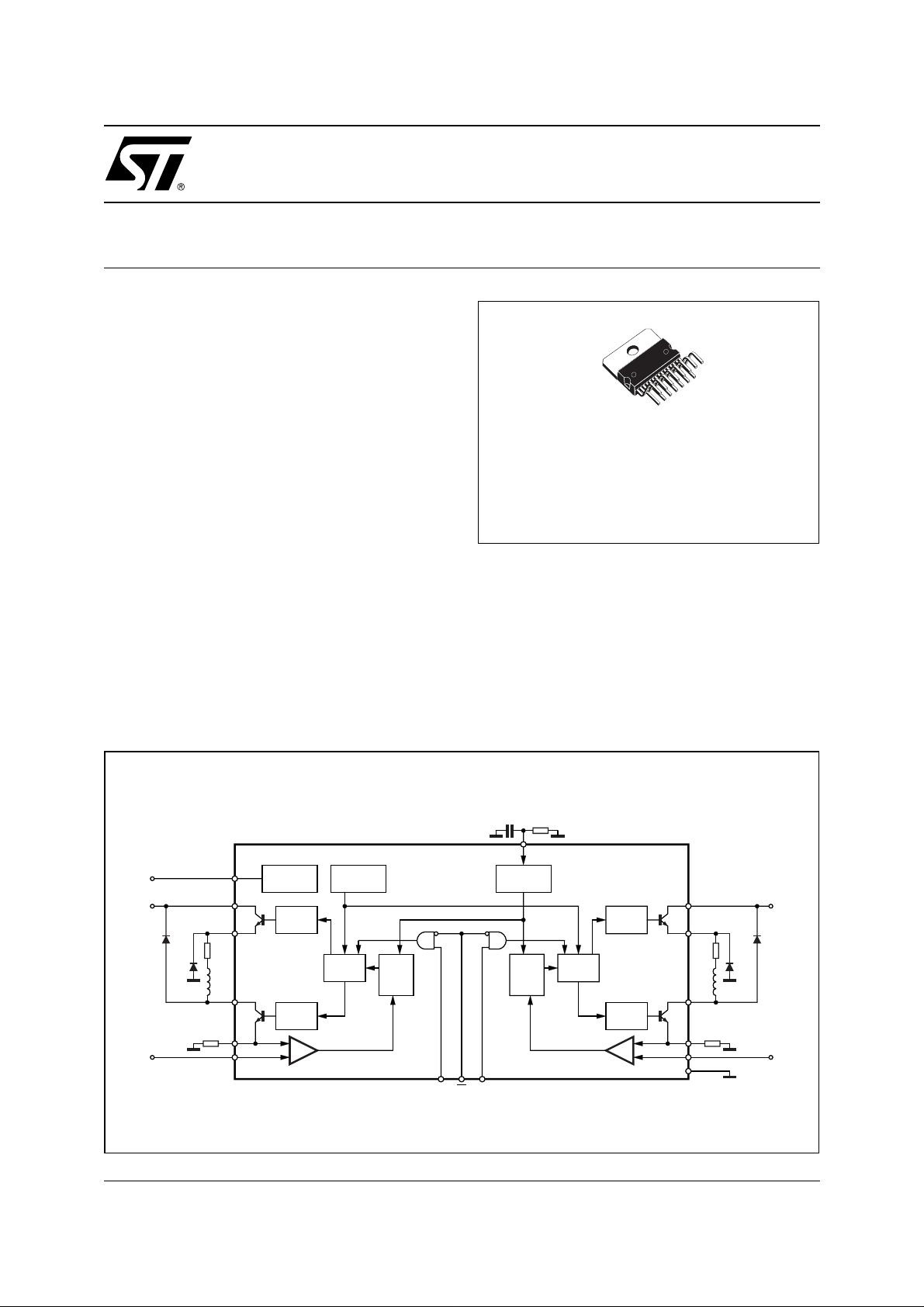
DUAL SWITCH-MODE SOLENOID DRIVER
■ HIGH CURRENT CAPABILITY (up to 2.5A per
channel)
■ HIGH VOLTAGE OPERATION (up to 46V for
power stage)
■ HIGH EFFICIENCY SWITCHMODE
OPERATION
■ REGULATED OUTPUT CURRENT
(adjustable)
■ FEW EXTERNAL COMPONENTS
■ SEPARATE LOGIC SUPPLY
■ THERMAL PROT EC T I O N
L295
MULTIWATT1 5
ORDERING NUMBER: L295
DESCRIPTION
The L295 is a monolithic integrated circuit in a 15
-lead Multiwatt® package; it incorporates all the
functions for direct interfacing between digital circuitry and inductive loads.
The L295 is designed to accept standard microprocessor logic levels at the inputs and can drive
2 solenoids. The output current is completely con-
BLOCK DIAGRAM
10
1
15
14
13
12
VOLTAGE
REGULATOR
H2
DRIVER
L2
DRIVER
+V
SS
+V
S
D3
R2
D4
L2
R
S2
V
REF2
THERMAL
SHUTDOWN
LOGIC
CIRCUITS
RR
Q
FF2 FF2
SS
1176
trolled by means of a switch-ing techniq ue allowing very efficient operation.
Furthermore, it includes an enable input and dual
supplies (for interfacing with peripherals running at
a higher voltage than the logic).
The L295 is particularly suitable for applications
such as hammer driving in matrix printers, step
motor driving and electromagnet controllers.
C
R
9
OSCILLATOR
1
H1
DRIVER
2
LOGIC
Q
CIRCUITS
L1
DRIVER
V
V
EN
in2
in1
D03IN1503
R1
L1
3
4
5
8
+V
S
D1
D2
V
REF1
October 2003
1/7
L295
ABSOLUTE MAXIMUM RATINGS
Symbol Parameter Value Unit
V
V
SS
V
EN
V
ref
I
o
P
tot
T
stg
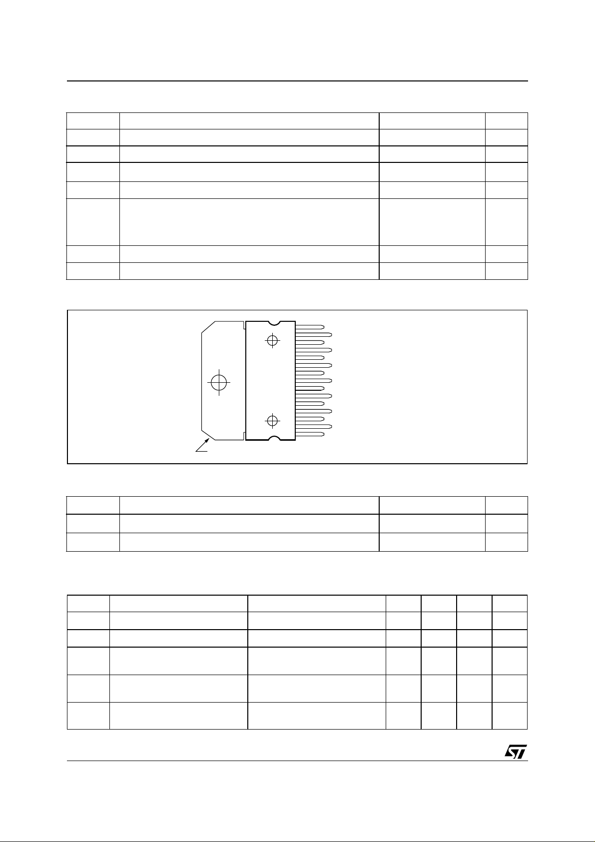
CONNECTION DIAGRAM
Supply voltage 50 V
S
Logic supply voltage 12 V
,
Enable and input voltage 7 V
V
i
Reference voltage 7 V
Peak output current (each channel)
- non repetitive (t = 100 µsec)
- repetitive (80% on - 20% off; T
- DC operation
Total power dissipation (at T
case
= 10ms)
on
= 75 ″C25W
3
2.5
2
, TjStorage and junction temperature - 40 to 150 °C
A
A
A
OUTPUT H ch 2
OUTPUT L ch 2
CURRENT SENSING 2
REFERENCE VOLTAGE 2
INPUT 2
LOGIC SUPPLY VOLTAGE V
OSCILLATOR RC NETWORK
GROUND
ENABLE
INPUT 1
REFERENCE VOLTAGE 1
CURRENT SENSING 1
OUTPUT L ch 1
OUTPUT H ch 1
SUPPLY VOLTAGE V
D03IN1502
SS
S
TAB CONNECTED TO PIN 8
15
14
13
12
11
10
9
8
7
6
5
4
3
2
1
THERMA L D ATA
Symbol Parameter Value Unit
R
th-j-case
R
th-j-amb
Thermal resistance junction-case
Thermal resistance junction-ambient
max 3
max 35
°C/W
°C/W
ELECTRICAL CHARACTERISTCS (Refer to the application circuit, Vss = 5V, Vs = 36V; Tj = 25°C;
L = Low; H = High; unless otherwise specified)
Symbol Parameter Test Condition Min. Typ. Max. Unit
V
V
I
V
i1
Supply Voltage 12 46 V
S
Logic Supply Voltage 4.75 10 V
SS
Quiescent Drain Current
I
d
(from V
Quiescent Drain Current
ss
(from V
,
Input Voltage Low
V
i2
SS
S
)
)
V
= 46V; Vi1 = Vi2 = VEN = L 4 mA
S
V
= 10V 46 mA
SS
-0.3
High
2.2
0.8
7
V
V
2/7
L295
ELECTRICAL CHARACTERISTCS (continued)
Symbol Parameter Test Condition Min. Typ. Max. Unit
V
I
i1
Enable Input Voltage Low
EN
,
Input Current Vi1 = Vi2 = L
I
i2
High
Vi1 = Vi2 = H
-0.3
2.2
0.8
7
-100
10
µA
µA
V
V
I
V
V
I
ref1
F
V
V
V
V
V
V
Enable Input Current VEN = L
EN
,
Input Reference Voltage 0.2 2 V
ref1
ref2
, I
Input Reference Voltage -5 µA
ref2
Oscillator Frequency C = 3.9 nF; R = 9.1 KΩ 25 46 KHz
osc
I
p
Transconductance (each ch.) V
ref
,
Input Reference Voltage 0.2 2 V
ref1
ref2
,
Input Reference Voltage 0.2 2 V
ref1
ref2
Total Output Voltage
drop
(each channel) (*)
V
,
External sensing resistors voltage
drop
= V
CEsat Q1
+ V
CEsat Q2
(*) V
sens1
V
sens2
drop
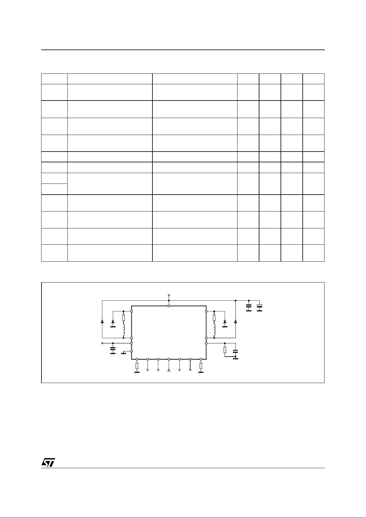
APPLICATION CIRCUIT
-100
= H
V
EN
= 1V 1.9 2 2.1 A/V
ref
I
o = 2 A
2.8 3.6 V
10
µA
µA
2V
.
+V
S
D2
D03IN1501
C2
0.1µF
D1
3.9nF
C3
+V
IN2
1
76
+V
EN
IN1
15
R2
D4
D3
L2
+V
SS
C1
0.1µF
10
8
13 12 11
R
S2
0.5Ω
+V
REF2
2
R1
L1
314
9
R3
9.1K
4
5
R
S1
0.5Ω
+V
REF1
C4
220µF
D2, D4 = 2A High speed diodes trr ≤ 200 ns
D1, D3 = 1A High speed diodes trr ≤ 200 ns
R1 = R2 = 2W
L1 = L2 = 5 mH
FUNCTIONAL DESCRIPTION
The L295 incorporates two indipendent driver channals with separate inputs and outputs, each capable of
driving an inductive load (see block diagram). The device is controlled by three micriprocessor compatible
digital inputs and two analog inputs.
3/7

L295
These inputs are:
– EN
chip enable (digital input, active low), enables both channels when in the low state.
– V
, V
in1
A channel is actived when both EN and the appropriate channel input are active.
channel inputs (digital inputs, active high), enable each channel independently.
in2
– V
, V
ref1
referce voltages (analog inputs), used to program the peak load currents. Peak load current
ref2
is proportional to V
ref
.
Since the two channels are identical, only channel one will be described. The following description applies
also the channel two, replacing FF2 for FF1, V
ref
for V
When the channel is avtivated by low level on the EN input and a high level on the channel input, V
ref1
etc.
in2
, the
output transistors Q1 and Q2 switch on and current flows in the load according to the exponential law:
V
I
------- - 1e
=
R1
R1t–
-------------–
L1
where:
R1 and R2 are the resistance and induct anc e of t he lo ad and V is the voltage available o n t he load (V
V
- V
drop
The current increases until the voltage on the external sens ing resistor, R
age, V
ref1
).
sense
. This peak current, Ip1, is given by:
V
p1
ref1
-------------=
R
S1
I
, reaches the reference vol t-
S1
s
At this point the comparator output, Vomp1, sete the RS flip-flop, FF1, that turns off the output transistor,
Q1. The load current flowing through D2, Q2, R
I
, decreases according to the law:
S1
V
A
------ - Ip1+
R
e
1
R1t–
-------------
L1
V
------- -–=
R1
A
-
where V
A
= V
CEsat Q2
+ V
sense
+ V
D2
If the oscillator pin (9) is connected to ground the load cur rent falls to zero as shown in fig. 1.
At this time t
the channel 1 is disabled, by taking the inputs V
2
low and/or EN high, and the output tran-
in1
sistor Q2 is turned off. The load current flows through D2 and D1 according to the law:
R1t–
-------------
L1
V
------- -–=
R1
B
where V
= VS + VD1 + V
B
D2
V
B
------- IT2+
I
R
1
e
IT2 = current value at the time t2.
Fig. 2 in shows the current waveform obtained with an RC network connected between pin 9 and ground.
From to t
the current increases as in fig.1. A difference exists at the time t2 because the current starts to
1
increase again. At this time a puls e is pr oduced by t he osc illa tor circ uit that res et s the flip. flo p, FF1, and
switches on the outout transistor, Q1. The current increases until the drop on the sensing resistor RS1 is
equal to V
(t3) and the cycle repeats.
ref1
The switching frequency depe nds on the value R an d C, as shown in fig. 4 and must be chosen in the
range 10 to 30 KHz. It is possible with external hardware to change the reference voltage V
obtain a high peak current I
and a lower holding current Ih (see fig. 3).
p
in order to
ref
The L295 is provided with a thermal protection that switches off all the output transistors when the junction
temperature exceeds 150°C. The presenc e of a hysteres is circuit makes the IC work again aftera fall of
4/7

L295
the junction temperature of about 20°C.
The analog input pins (V
an internal reference voltage of about 2.5V and the peak current in the load is fixed only by the value of R
ref1
, V
) can be left open or connected to Vss; in thi s ca se the circui t wo r ks with
ref2
2.5
I
P
--------=
R
S
:
s
SIGNAL WAVEFOR MS
Figure 1. Load c ur re nt waveform wit h pi n 9
connected to GND.
I
I
P
t
Vi ⋅ EN
V
Q1
Q2
REF
ON
OFF
ON
OFF
t
0
1
t
2
D03IN1504
t
t
t
t
t
Figure 2. Load current waveform with external
R-C network connected between pin 9 and
ground.
I
I
P
Figure 3. With V
I
I
p
I
n
Vi ⋅ EN
V
REF
ON
Q1
OFF
ON
Q2
OFF
changed by hardware.
ref
t
0t1t2t3
t
n
D03IN1506
t
t
t
t
t
Figure 4. Switching frequency vs. values of R
and C.
f
(KHz)
D03IN1507
Vi ⋅ EN
V
Q1
Q2
REF
ON
OFF
ON
OFF
fo=25KHz
t1t2t3t
t
0
tnt
4
5
D03IN1505
t
t
t
t
t
10
6.8nF
15nF
Rmin
1
1 10 100 R(KΩ)
3.9nF
2.2nF
C=1nF
5/7

L295
DIM.
MIN. TYP. MAX. MIN. TYP. MAX.
A 5 0.197
B 2.65 0.104
C 1.6 0.063
D 1 0.039
E 0.49 0.55 0.019 0.022
F 0.66 0.75 0.026 0.030
G 1.02 1.27 1.52 0.040 0.050 0.060
G1 17.53 17.78 18.03 0.690 0.700 0.710
H1 19.6 0.772
H2 20.2 0.795
L 21.9 22.2 22.5 0.862 0.874 0.886
L1 21.7 22.1 22.5 0.854 0.870 0.886
L2 17.65 18.1 0.695 0.713
L3 17.25 17.5 17.75 0.679 0.689 0.699
L4 10.3 10.7 10.9 0.406 0.421 0.429
L7 2.65 2.9 0.104 0.114
M 4.25 4.55 4.85 0.167 0.179 0.191
M1 4.63 5.08 5.53 0.182 0.200 0.218
S 1.9 2.6 0.075 0.102
S1 1.9 2.6 0.075 0.102
Dia1 3.65 3.85 0.144 0.152
mm inch
OUTLINE AND
MECHANICAL DATA
Multiwatt15 V
6/7

L295
Information furnished is believed to be accurate and reliable. However, STMicroelectronics assumes no responsibility for the consequences
of use of such information nor for any infringement of patents or other rights of third parties which may result from its use. No license is granted
by implic ation or otherwise under any patent or patent r i ght s of STMi croelectr oni cs. Spec i fications mentioned i n this publication are subject
to change without notice. This publication supersedes and replaces all information previously supplied. STMicroelectronics product s are not
authorized for use as cri tical comp onents in lif e support devi ces or systems without express written approva l of STMicroel ectronics.
The ST logo is a registered trademark of STMicroelectr oni cs.
All other n am es are the property of th ei r respectiv e owners
© 2003 STMi croelectronics - All rights reserved
Australi a - B elgium - Brazil - Canada - China - C zech Republi c - Finland - F rance - Germ any - Hong Kong - India - Is rael - Italy - Japan -
Malaysia - Malta - Morocco - Singapore - Spain - Sweden - Switzerland - United Kingdom - United States
STMicroelectronics GROUP OF COMPANIES
www.st.com
7/7
 Loading...