

PUSH-PULL FOUR CHANNEL DRIVERS
■ OUTPUT CURRENT 1A PER CHANNEL
■ PEAK OUTPUT CURRENT 2A PER CHANNEL
(non repetitive)
■ INHIBIT FACILITY
■ HIGH NOISE IMMUNITY
■ SEPARATE LOGIC SUPPLY
■ OVERTEMPE R ATURE PR O TECTION
L293B
L293E
DIP16 POWERDIP(16 +2+2)
DESCRIPTION
The L293B and L293E are quad push-pull drivers
capable of delivering output currents to 1A per
channel. Each channel is controlled by a TTLcompatible logic input and each pair of drivers (a
full bridge) is equipped with an inhibit input which
turns off all four transistors. A separate supply input is provided for the logic so that it may be run
off a lower voltage to reduce dissipation.
Additionally, the L293E has external connection of
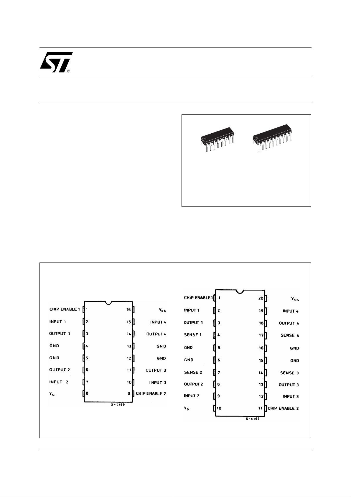
PIN CONNECTION (Top view)
DIP16 - L293B
ORDERING NUMBERS:
L293B L293E
sensing resistors, for switchmode control.
The L293B and L293E are pac kage in 16 and 20-
pin plastic DIPs respectively ; both use the four
center pins to conduct heat to the printed circuit
board.
POWERDIP (1 6+2 +2) - L293E
July 2003
1/12
L293E L293B
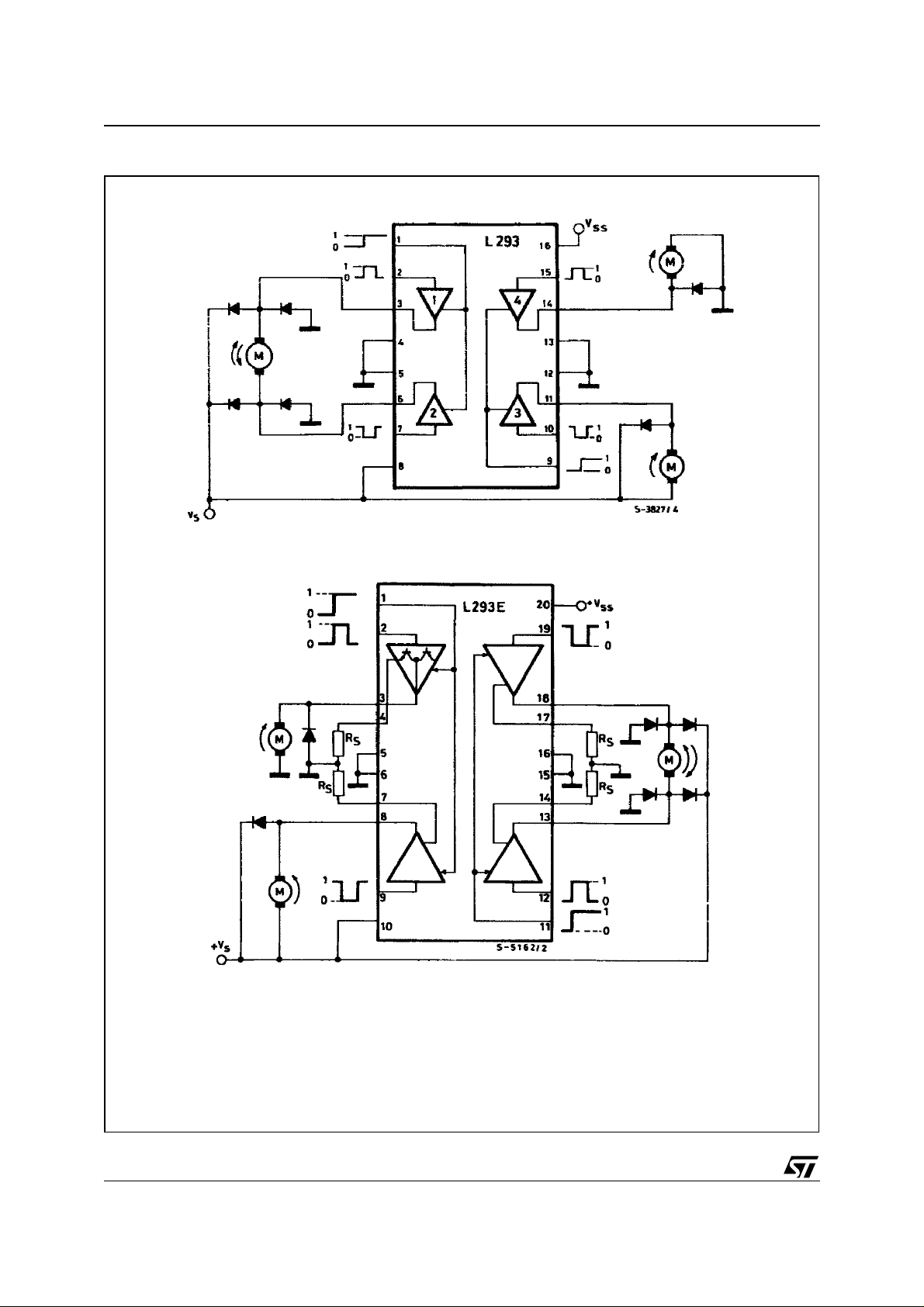
BLOCK DIAGRAMS
DIP16 - L293B
POWERDIP (1 6+2 +2) - L293E
2/12
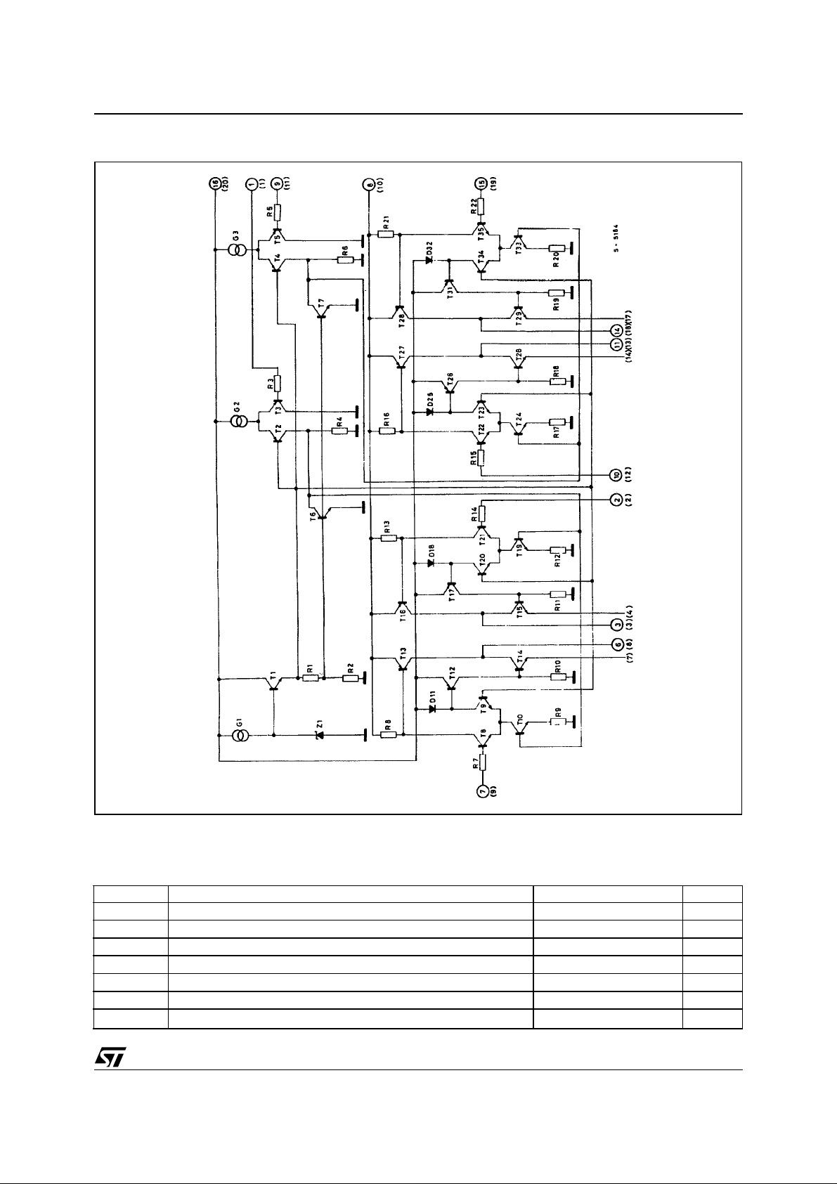
SCHEMATIC DIAGRAM
L293E L293B
(*) In the L293 these point s are not externally avai l able. They are i nternall y connected to the ground (substrat e).
O Pins of L293 () Pins of L293E.
ABSOLUTE MAXIMUM RATINGS
Symbol Parameter Value Unit
V
V
ss
V
V
inh
I
out
P
tot
T
stg
Supply Voltage 36 V
s
Logic Supply Voltage 36 V
Input Voltage 7 V
i
Inhibit Voltage 7 V
Peak Output Current (non repetitive t = 5ms) 2 A
Total Power Dissipation at T
ground-pins
= 80°C 5 W
, TjStorage and Junction Temperature –40 to +150
o
C
3/12
L293E L293B
THERMA L D ATA
Symbol Parameter Value Unit
R
th j-case
R
th j-amb
Thermal Resistance Junction-case Max. 14
Thermal Resistance Junction-ambient Max. 80
ELECTRICAL CHARACTERISTCS
Symbol Parameter Test Condition Min. Typ. Max. Unit
V
Supply Voltage
s
V
Logic Supply Voltage 4.5 36 V
ss
I
Total Quiescent Supply Current Vi = L; Io = 0; V
s
Total Quiescent Logic Supply
I
ss
Current
V
ViH
V
V
I
inhL
I
inhH
V
CEsatH
V
CEsatL
V
SENS
t
t
* See figure 1
** Referred to L293E
Input Low Voltage -0.3 1.5 V
iL
Input High Voltage VSS ≤ 7V 2.3
Low Voltage Input Current
I
iL
High Voltage Input Current 2.3V ≤ VIH ≤ VSS - 0.6V 30 100 µA
I
iH
Inhibit Low Voltage -0.3 1.5 V
inhL
Inhibit High Voltage VSS ≤7V 2.3
inhH
Low Voltage Inhibit Current V
High Voltage Inhibit Current 2.3V ≤V
Source Output Saturation Voltage Io = -1A 1.4 1.8 V
Sink Output Saturation Voltage Io = 1A 1.2 1.8 V
Sensing Voltage (pins 4, 7, 14, 17)
t
Rise Time 0.1 to 0.9 Vo (*) 250 ns
r
t
Fall Time 0.9 to 0.1 Vo (*) 250 ns
f
Turn-on Delay 0.5 Vi to 0.5 Vo (*) 750 ns
on
Turn-off Delay 0.5 Vi to 0.5 Vo (*) 200 ns
off
= h; Io = 0; V
V
i
Vi = L; Io = 0; V
= h; Io = 0; V
V
i
V
> 7V
SS
V
= 1.5V
il
V
> 7V
SS
inhL
(**)
= H 2 6 mA
inh
= H 16 24 mA
inh
V
= L 4 mA
inh
= H 44 60 mA
inh
= H 16 22 mA
inh
V
= L 16 24 mA
inh
= 1.5V -30 -100 µA
≤ Vss- 0.6V ±10 µA
inhH
V
ss
2.3 7 V
2.3 7 V
o
o
36 V
Vss V
-10 µA
V
ss
2V
C/W
C/W
V
TRUTH TABLE
V
(each channel) V
i
HHH
LLH
H
L
(*) High output impedan ce
(**) Relative to the considerate c hannel
4/12
X
X
o
(*)
(*)
(**)
V
inh
L
L

Figure 1. Swi tc hing Timers
L293E L293B
Figure 2. Saturation voltage versus Output
Current
Figure 3. Source Saturation Voltage versus
Ambient Temperature
Figure 4. Sink Saturation Voltage versus
Ambient Temperatu re
Figure 5. Quiescent Logic Supply Current
versus Logic Supply Voltage
5/12

L293E L293B
Figure 6. Output Voltage versus Inpu t Voltage
Figure 7. Output Voltage versus Inhibit Voltage
APPLICATION INFORMATION
Figure 8. DC Mo t or Controls
(with connection to ground and to the
supply voltage)
V
AM1B M2
inh
HH
H L Run L Fast Motor Stop
L X Free Running X Free Running
Fast M otor Stop
HRun
Motor Stop Motor Stop
L = Low H = High X = Don’t Care
Figure 9. Bidirectional DC Motor Control
Inputs Function
= H C = H ; D = L Turn Right
V
inh
C = L ; D = H Turn Left
C = D Fast Motor Stop
V
= L C = X ; D = X Free Running Motor Stop
inh
L = Low H = High X = Don’t Care
6/12

Figure 10. Bi pol ar S te pp in g Motor Cont rol
L293E L293B
7/12

L293E L293B
Figure 11. Stepping Motor Driver with Phase Curren t Control and Short Circui t Protection
8/12
L293E L293B
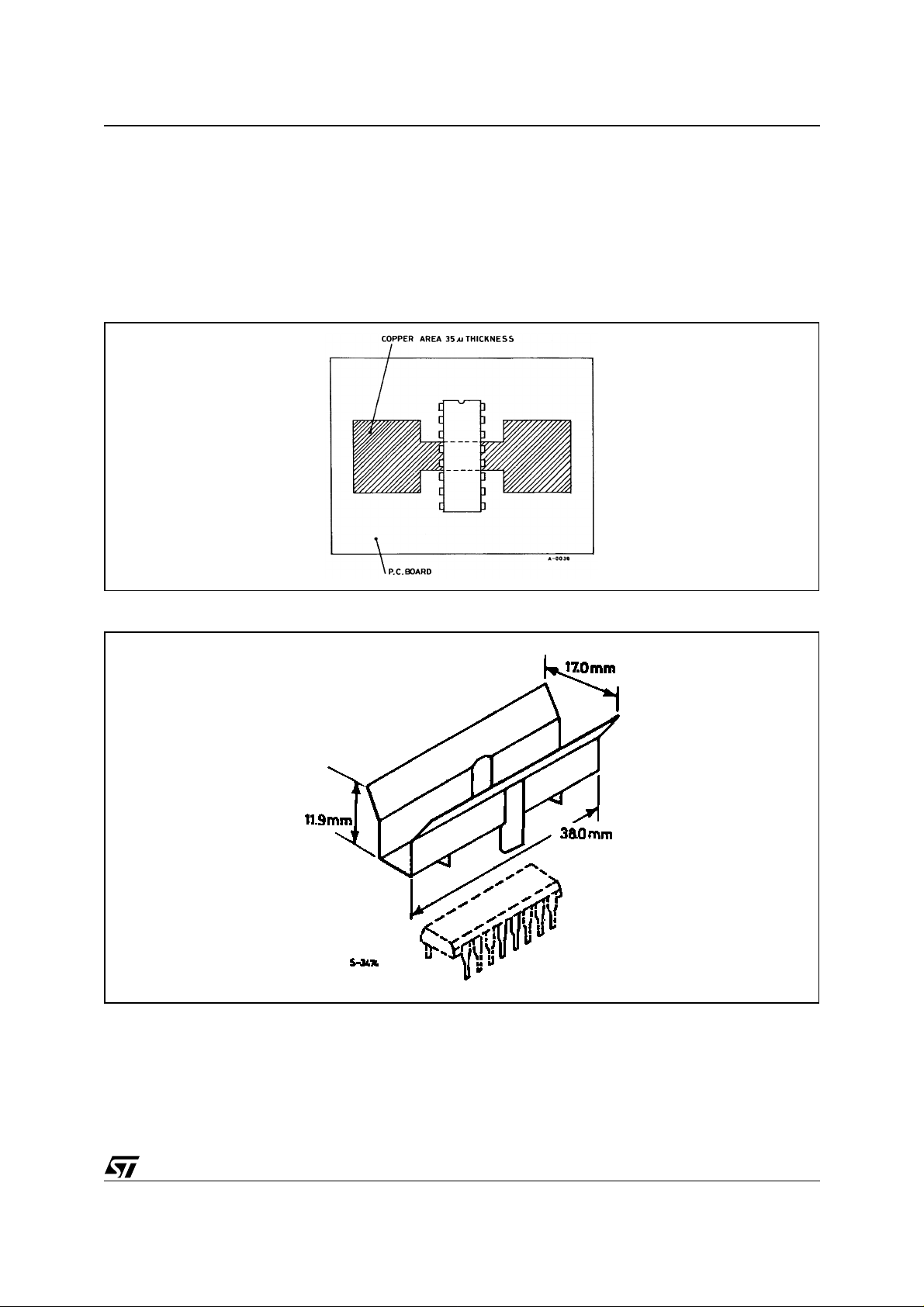
MOUNTING INSTRUCTIONS
The R
area of the printed circuit board as shown in figure 12 or to an external heatsink (figure 13).
During soldering the pins temperature must not exceed 260°C and the soldering time must not be longer
than 12 seconds.
The external heatsink or printed circuit copper area must be connected to electrical ground.
Figure 12. Example of P.C. Board Copper Area which is Used as Heatsink
of the L293B and the L293E can be reduced by soldering the GND pins to a suitable copper
th j-amb
Figure 13. External Heatsink Mounting Examp le (R
= 30°C/W)
th
9/12

L293E L293B
DIM.
MIN. TYP. MAX. MIN. TYP. MAX.
a1 0.51 0.020
B 0.77 1.65 0.030 0.065
b 0.5 0.020
b1 0.25 0.010
D 20 0.787
E 8.5 0.335
e 2.54 0.100
e3 17.78 0.700
F 7.1 0.280
I 5.1 0.201
L 3.3 0.130
Z 1.27 0.050
mm inch
OUTLINE AND
MECHANICAL DATA
DIP16
10/12

L293E L293B
DIM.
MIN. TYP. MAX. MIN. TYP. MAX.
a1 0.51 0.020
B 0.85 1.40 0.033 0.055
b 0.50 0.020
b1 0.38 0.50 0.015 0.020
D 24.80 0.976
E 8.80 0.346
e 2.54 0.100
e3 22.86 0.900
F 7.10 0.280
I 5.10 0.201
L 3.30 0.130
Z 1.27 0.050
mm inch
OUTLINE AND
MECHANICAL DATA
Powerdip 20
11/12

L293E L293B
Information furnished is believed to be accurate and reliable. However, STMicroelectronics assumes no responsibility for the consequences
of use of such information nor for any infringement of patents or other rights of third parties which may result from its use. No license is granted
by implic ation or otherwise under any patent or patent r i ght s of STMi croelectr oni cs. Specifications mentioned in th i s publicati on are subject
to change without notice. This publication supersedes and replaces all information previously supplied. STMicroelectronics products are not
authorized for use as cri tical components in life support devices or syst ems witho ut express wri t ten approval of STMicroelectronics.
STMicroelectronics acknowl edges the trademarks of all companies referred to in this do cument.
The ST logo is a registered trademark of STMicroelectronics
© 2003 STMic roelectroni cs - All Rig hts Reserved
Austra lia - Brazil - Canada - Ch i na - F i nl and - France - Germany - Hong Kong - India - Israel - Italy - Japa n -Malaysia - Malta - Morocco -
Singap ore - Spain - Sw eden - Switzerland - Uni ted Kingdom - United St ates.
STMicroelectronics GROUP OF COMPANIES
http://www.s t. com
12/12
 Loading...