

Push-pull four channel driver with diodes
Features
■ 600 mA output current capability per channel
■ 1.2 A peak output current (non repetitive) per
channel
■ Enable facility
■ Overtemperature protection
■ Logical “0” input voltage up to 1.5 V (high noise
immunity)
■ Internal clamp diodes
Description
The device is a monolithic integrated high voltage,
high current four channel driver designed to
accept standard DTL or TTL logic levels and drive
inductive loads (such as relays solenoides, DC
and stepping motors) and switching power
transistors.
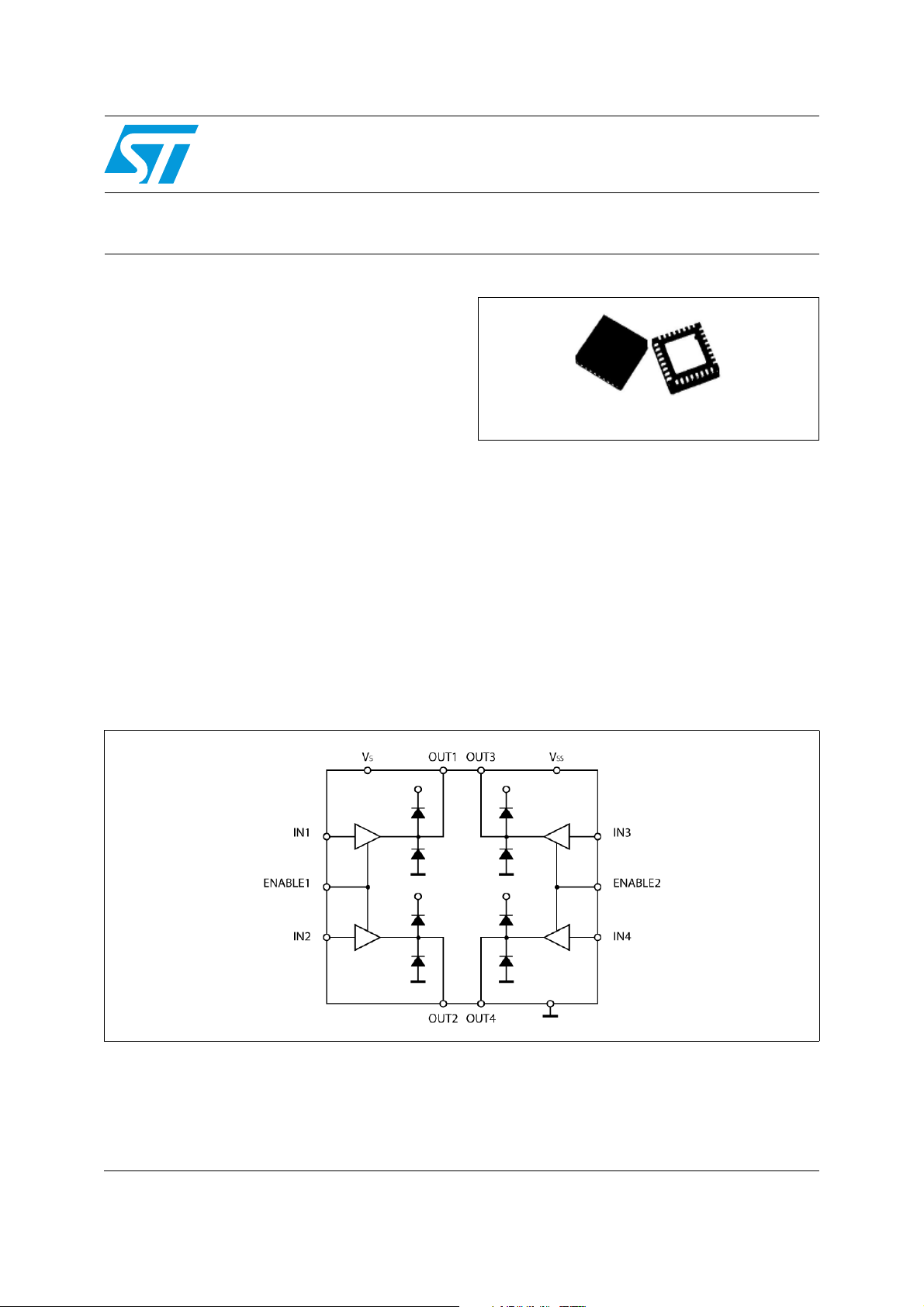
L2293Q
VFQFPN 5 mm x 5 mm 32L
To simplify use as two bridges each pair of
channels is equipped with an enable input. A
separate supply input is provided for the logic,
allowing operation at a lower voltage and internal
clamp diodes are included.
This device is suitable for use in switching
applications at frequencies up to 50 kHz.
The L2293Q is assembled in a VFQFPN-32L 5x5
package which has exposed pad available for
heatsinking.
Figure 1. Block diagram
August 2009 Doc ID 14899 Rev 3 1/13
www.st.com
13

Contents L2293Q
Contents
1 Electrical data . . . . . . . . . . . . . . . . . . . . . . . . . . . . . . . . . . . . . . . . . . . . . . 3
1.1 Absolute maximum ratings . . . . . . . . . . . . . . . . . . . . . . . . . . . . . . . . . . . . . 3
1.2 Recommended conditions . . . . . . . . . . . . . . . . . . . . . . . . . . . . . . . . . . . . . 3
1.3 Thermal data . . . . . . . . . . . . . . . . . . . . . . . . . . . . . . . . . . . . . . . . . . . . . . . 4
2 Pin connection . . . . . . . . . . . . . . . . . . . . . . . . . . . . . . . . . . . . . . . . . . . . . . 5
3 Electrical characteristics . . . . . . . . . . . . . . . . . . . . . . . . . . . . . . . . . . . . . 7
4 Package mechanical data . . . . . . . . . . . . . . . . . . . . . . . . . . . . . . . . . . . . . 9
5 Order codes . . . . . . . . . . . . . . . . . . . . . . . . . . . . . . . . . . . . . . . . . . . . . . . 11
6 Revision history . . . . . . . . . . . . . . . . . . . . . . . . . . . . . . . . . . . . . . . . . . . 12
2/13 Doc ID 14899 Rev 3
L2293Q Electrical data
1 Electrical data
1.1 Absolute maximum ratings
Table 1. Absolute maximum ratings
Symbol Parameter Value Unit
V
V
V
P
T
Supply voltage 36 V
S
Logic supply voltage 36 V
SS
V
Input voltage 7 V
i
Enable voltage 7 V
en
Peak output current (100 μs non repetitive) 1.2 A
I
o
Total power dissipation at T
tot
Junction temperature 150 °C
T
J
Storage temperature – 40 to 150 °C
STG
pins
1.2 Recommended conditions
Table 2. Recommended conditions
Symbol Parameter
V
V
T
1. See Figure 2
Supply voltage V
S
Logic supply voltage 2.8
SS
Junction temperature -20
J
= 90 °C 4 W
Value
Unit
Min Typ Max
SS
(1)
(1)
36 V
36 V
125 °C
Doc ID 14899 Rev 3 3/13
Electrical data L2293Q
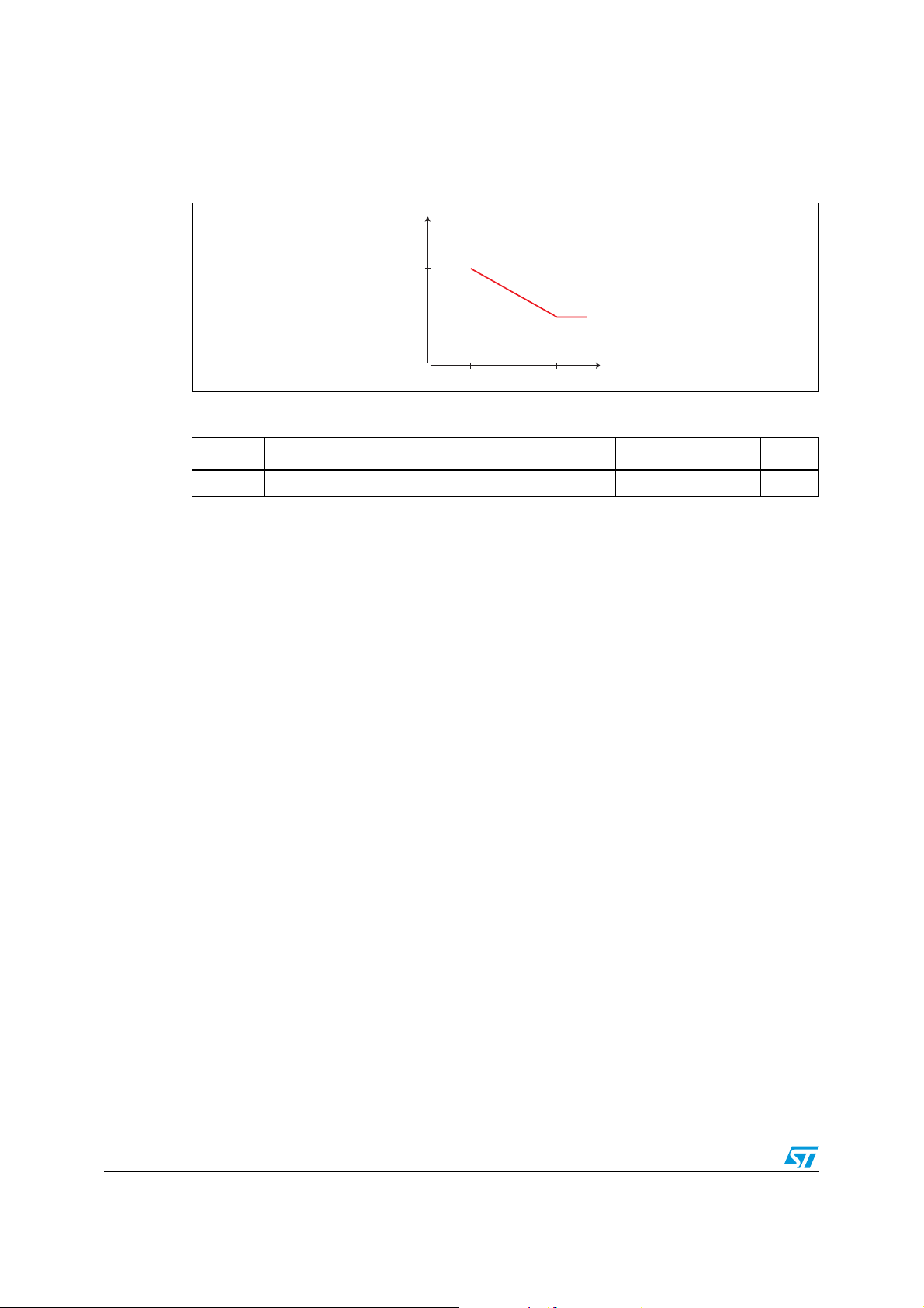
1.3 Thermal data
Figure 2. Typical minimum logic supply voltage vs junction temperature
V
SS_min
[V]
2.8
2.7
T
j
0-10-20
Table 3. Thermal data
Symbol Parameter Value Unit
R
th(JA)
1. Mounted on a double-layer FR4 PCB with a dissipating copper surface of 0.5 cm2 on the top side plus
6 cm2 ground layer connected through 18 via holes (9 below the IC).
Thermal resistance junction-ambient max.
(1)
[°C]
42 °C/W
4/13 Doc ID 14899 Rev 3

L2293Q Pin connection
BOTTOM LAYER
(connected to GND)
TOP LAYER
(connected to GND)
L2293Q
2 Pin connection
Figure 2. Pin connection (top view)
Note: NC
The exposed PAD must be connected to GND pins.
NC
Figure 3. Recommended PCB layout for R
(1)
These NC pins are connected to the exposed PAD.
(2)
These NC pins can be connected to GND pins and exposed PAD.
optimization
th(JA)
L2293Q
TOP LAYER
(connected to GND)
GND pins
BOTTOM LAYER
VIA holes
(connected to GND)
Doc ID 14899 Rev 3 5/13

Pin connection L2293Q
Table 4. Pin description
Pin n° Name Type Function
1, 18, 19, 20,
21, 22, 23
NC Not connected
2, 3, 4, 5, 6, 7, NC Pins connected to the exposed PAD
8, 9, 17, 24, 28,
32
GND Ground
10 OUTPUT2 O Output 2
11 INPUT2 I Input 2
Supply voltage for the power output stages. A non-inductive
12, 13 V
S
100 nF capacitor must be connected between these pins and
ground.
14 ENABLE2 I
Enable 2 input, the LOW state disables the Output 3 and
Output 4.
15 INPUT3 I Input 3
16 OUTPUT3 O Output 3
25 OUTPUT4 O Output 4
26 INPUT4 I Input 4
27 V
SS
29 ENABLE1 I
Supply voltage for the logic blocks. A 100 nF capacitor must
be connected between this pin and ground.
Enable 1 input, the LOW state disables the output 1 and
Output 2.
30 INPUT1 I Input 1
31 OUTPUT1 O Output 1
6/13 Doc ID 14899 Rev 3

L2293Q Electrical characteristics
3 Electrical characteristics
For each channel, VS = 24 V, VSS = 5 V, TA = 25 °C, unless otherwise specified.
Table 5. Electrical characteristics
Symbol Pin Parameter Test condition Min Typ Max Unit
V
= L; IO = 0; Ven = H 2 6 mA
i
I
I
SS
V
V
I
I
V
en L
V
en H
I
en L
I
en H
V
CE(sat)H
V
CE(sat)L
V
S
IL
IH
IL
IH
F
12,13 Total quiescent supply current
27
Total quiescent logic supply
current
11, 15,
26, 30
11, 15,
26, 30
11, 15,
26, 30
11, 15,
26, 30
Input low voltage – 0.3 1.5 V
Input high voltage
Low voltage input current V
High voltage input current 2.3 V ≤ V
= H; IO = 0; Ven = H 16 24 mA
V
i
V
= L 4 mA
en
Vi = L; IO = 0; Ven = H 44 60 mA
= H; IO = 0; Ven = H 16 22 mA
V
i
V
= L 16 24 mA
en
V
≤ 7 V 2.3 V
SS
> 7 V 2.3 7 V
V
SS
= 1.5 V – 10 μA
IL
≤ VSS – 0.6 V 30 100 μA
IH
SS
14, 29 Enable low voltage – 0.3 1.5 V
V
≤ 7 V 2.3
14, 29 Enable high voltage
14, 29 Low voltage enable current V
SS
V
> 7 V 2.3 7 V
SS
= 1.5 V – 30 – 100 μA
en L
14, 29 High voltage enable current 2.3 V ≤ V
10, 16,
25, 31
10, 16,
25, 31
Source output saturation voltage I
Sink output saturation voltage I
= – 0.6 A 1.4 1.8 V
O
= + 0.6 A 1.2 1.8 V
O
≤ VSS – 0.6 V ± 10 μA
en H
V
SS
Clamp diode forward voltage IO = 600 nA 1.3 V
V
V
Doc ID 14899 Rev 3 7/13

Electrical characteristics L2293Q
VS = 24 V, VSS = 5 V, TA = 25 °C, unless otherwise specified.
Table 6. AC operation
Symbol Parameter Test condition Min Typ Max Unit
t
r Rise time
Fall time
t
f
t
t
1. See Figure 4
on
off
Turn-on delay
Turn-off delay
(1)
(1)
(1)
(1)
0.1 to 0.9 V
0.9 to 0.1 V
O
O
0.5 Vi to 0.5 V
0.5 Vi to 0.5 V
250 ns
250 ns
O
O
750 ns
200 ns
Figure 4. Switching times
Table 7. Truth table (one channel)
Input Enable
HH H
LH L
HLZ
LLZ
1. Relative to the considered channel
2. Z = High output impedance
(1)
Output
(2)
(2)
8/13 Doc ID 14899 Rev 3

L2293Q Package mechanical data
4 Package mechanical data
In order to meet environmental requirements, ST offers these devices in different grades of
ECOPACK
®
packages, depending on their level of environmental compliance. ECOPACK®
specifications, grade definitions and product status are available at: www.st.com.
ECOPACK is an ST trademark.
Table 8. VFQFPN 5x5x1.0 32L pitch 0.50
Databook (mm)
Dim.
Min Typ Max
A 0.80 0.85 0.95
b 0.18 0.25 0.30
b1 0.165 0.175 0.185
D 4.85 5.00 5.15
D2 3.00 3.10 3.20
D3 1.10 1.20 1.30
E 4.85 5.00 5.15
E2 4.20 4.30 4.40
E3 0.60 0.70 0.80
e0.50
L 0.30 0.40 0.50
ddd 0.08
Note: 1 VFQFPN stands for thermally enhanced very thin profile fine pitch quad flat package no
lead. Very thin profile: 0.80 < A ≤ 1.00 mm.
2 Details of terminal 1 are optional but must be located on the top surface of the package by
using either a mold or marked features.
Doc ID 14899 Rev 3 9/13

Package mechanical data L2293Q
Figure 5. Package dimensions
10/13 Doc ID 14899 Rev 3

L2293Q Order codes
5 Order codes
Table 9. Order code
Order code Package Packaging
L2293Q VFQFPN 5x5x1.0 32L Tube
Doc ID 14899 Rev 3 11/13

Revision history L2293Q
6 Revision history
Table 10. Document revision history
Date Revision Changes
10-Jul-2008 1 First release
26-Feb-2009 2 Updated Table 3 on page 4
12-Aug-2009 3 Updated description in coverpage
12/13 Doc ID 14899 Rev 3

L2293Q
Please Read Carefully:
Information in this document is provided solely in connection with ST products. STMicroelectronics NV and its subsidiaries (“ST”) reserve the
right to make changes, corrections, modifications or improvements, to this document, and the products and services described herein at any
time, without notice.
All ST products are sold pursuant to ST’s terms and conditions of sale.
Purchasers are solely responsible for the choice, selection and use of the ST products and services described herein, and ST assumes no
liability whatsoever relating to the choice, selection or use of the ST products and services described herein.
No license, express or implied, by estoppel or otherwise, to any intellectual property rights is granted under this document. If any part of this
document refers to any third party products or services it shall not be deemed a license grant by ST for the use of such third party products
or services, or any intellectual property contained therein or considered as a warranty covering the use in any manner whatsoever of such
third party products or services or any intellectual property contained therein.
UNLESS OTHERWISE SET FORTH IN ST’S TERMS AND CONDITIONS OF SALE ST DISCLAIMS ANY EXPRESS OR IMPLIED
WARRANTY WITH RESPECT TO THE USE AND/OR SALE OF ST PRODUCTS INCLUDING WITHOUT LIMITATION IMPLIED
WARRANTIES OF MERCHANTABILITY, FITNESS FOR A PARTICULAR PURPOSE (AND THEIR EQUIVALENTS UNDER THE LAWS
OF ANY JURISDICTION), OR INFRINGEMENT OF ANY PATENT, COPYRIGHT OR OTHER INTELLECTUAL PROPERTY RIGHT.
UNLESS EXPRESSLY APPROVED IN WRITING BY AN AUTHORIZED ST REPRESENTATIVE, ST PRODUCTS ARE NOT
RECOMMENDED, AUTHORIZED OR WARRANTED FOR USE IN MILITARY, AIR CRAFT, SPACE, LIFE SAVING, OR LIFE SUSTAINING
APPLICATIONS, NOR IN PRODUCTS OR SYSTEMS WHERE FAILURE OR MALFUNCTION MAY RESULT IN PERSONAL INJURY,
DEATH, OR SEVERE PROPERTY OR ENVIRONMENTAL DAMAGE. ST PRODUCTS WHICH ARE NOT SPECIFIED AS "AUTOMOTIVE
GRADE" MAY ONLY BE USED IN AUTOMOTIVE APPLICATIONS AT USER’S OWN RISK.
Resale of ST products with provisions different from the statements and/or technical features set forth in this document shall immediately void
any warranty granted by ST for the ST product or service described herein and shall not create or extend in any manner whatsoever, any
liability of ST.
ST and the ST logo are trademarks or registered trademarks of ST in various countries.
Information in this document supersedes and replaces all information previously supplied.
The ST logo is a registered trademark of STMicroelectronics. All other names are the property of their respective owners.
© 2009 STMicroelectronics - All rights reserved
STMicroelectronics group of companies
Australia - Belgium - Brazil - Canada - China - Czech Republic - Finland - France - Germany - Hong Kong - India - Israel - Italy - Japan -
Malaysia - Malta - Morocco - Philippines - Singapore - Spain - Sweden - Switzerland - United Kingdom - United States of America
www.st.com
Doc ID 14899 Rev 3 13/13
 Loading...