

250 W microinverter for plug-in PV panels
Features
■ Input voltage range from 18 V to 45 V
■ Output voltage range from 110 V to 240 V AC,
50/60 Hz
■ Grid connection algorithm and MPPT capability
■ Digital control section managed by the STM32
■ Reactive power management
■ RS-232 for communication
■ RoHS compliant
Description
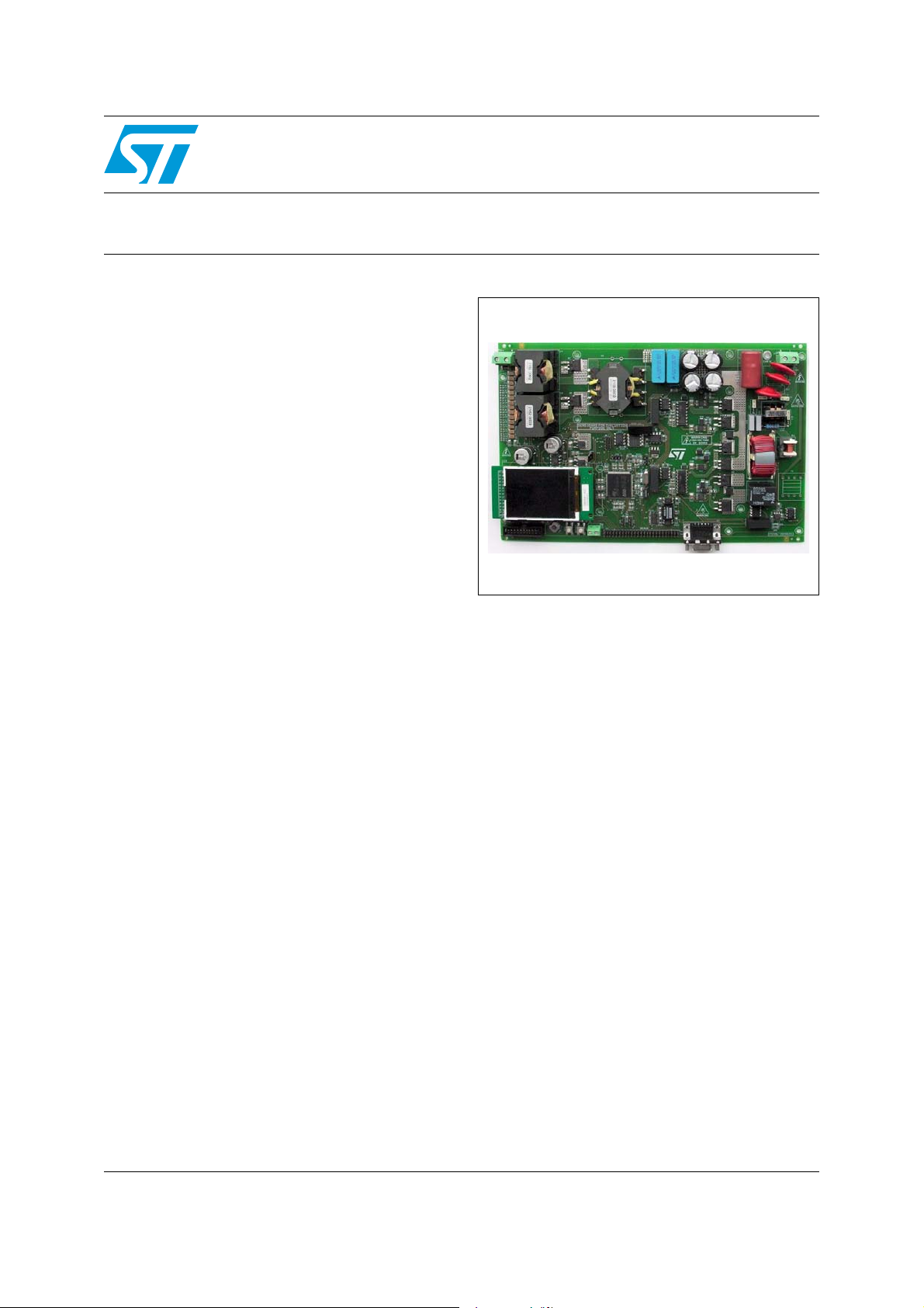
STEVAL-ISV003V1
demonstration board
Data brief
The STEVAL-ISV003V1 is a demonstration board
which implements the microinverter concept and
is designed to optimize the power production of
each single solar panel by means of DC/AC
conversion. The conversion system is capable of
both grid synchronization and Maximum Power
Point Tracking (MPPT) thanks to the use of an
advanced control algorithm implemented in the
32-bit STM32 microcontroller. The MPPT function
is based on the perturb and observe (P & O)
concept which seeks the best operating point of
the panel, thus maximizing the energy produced
under any environmental condition. The grid
synchronization algorithm has the advantage over
standard solutions of a decoupled control of
active and reactive power. The STEVALISV003V1 demonstration board uses a highfrequency (HF) isolated DC/DC converter with
interleaved current and an optimized full-bridge
DC/AC inverter. The typical solar panel voltage is
first stepped up to about 400 V and then
converted into AC to create a sinusoidal output.
An LED display provides a user-friendly interface
for the end user which allows monitoring and/or
modifying some of the main operating
parameters. Two modes of operation are available
and can be selected to allow either open-loop
operation or closed-loop operation in
synchronization with the grid.
STEVAL-ISV003V1
In open-loop mode the sinusoidal reference is
created internally by means of a standard lookup
table, while in closed-loop mode, a sinusoidal
voltage feedback, proportional to the grid voltage,
is used. The system can be connected to either a
50 Hz or 60 Hz network, depending on local
requirements. Finally, the RS-232 interface can be
used for serial data transfer of specified voltage,
current and current signals.
October 2011 Doc ID 022334 Rev 2 1/12
For further information contact your local STMicroelectronics sales office.
www.st.com
12
Schematics STEVAL-ISV003V1
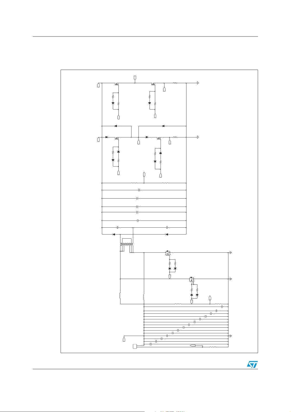
1 Schematics
Figure 1. Isolated interleaved boost converter
0.02/0.5W
STB42N65M5
Q2
R21
27/0.25W
OUT AC 2
LOW FREQUENCYHIGH FREQUENCY
R2
D10
3.3/0.25W
STB42N65M5
Q4
R23
27/0.25W
R5
D15
3.3/0.25W
R14
SENS LE G2
Low f PWM High Side 2
D11
STPSC606
6A
600V
STPS3L40S
D6
Q1
STB42N65M5
DRAIN MO SFE T HIGH 1 DRAIN MOSFET HIGH 2
R19
27/0.25W
R1
D9
2.2uF, 250V
C13
12
D40
STPSC806G
6
D16
3.3/0.25W
High f PWM High Side 1
9
542
OUT AC 1
Vbus_SENS
R3
15M 1%
C11
22uF, 450V
C10
22uF, 450V
C9
22uF,450V
C8
22uF, 450V
C7
2.2uF, 630V
7
10
T3
TRAFO
1
3
FUNCTIONAL ISOLATION
Low f PWM Low Side 2
D34
STPSC606
D17
3.3/0.25W
High f PWM Low Side 1
R6
Q5
0.02/0.5W
R11
SENS LE G1
100k 1%
C12
2.2uF, 250V
D42
STPSC806G
STH180N10F3-2
D8
STPS3L40S
Q3
STB42N65M5
R20
27/0.25W
R4
D14
800uH 4A
L4 INDUCTOR
Magnetica
1
VINPUT
2
J1
CON_ PV
2/12 Doc ID 022334 Rev 2
R9 27/ 0.2 5W
2.7/0.25W
D21 R7
D23
Schottky
Gate 2
800uH 4A
Magnetica
L6 INDUCTOR
1uF, 100V
C19
1uF, 100V
C18
C17
1uF, 100V
C16
1uF, 100V
C15
1uF, 100V
STH180N10F3-2
Q7
R12 27/0.25W
2.7/0.25W
D22 R8
D24
1uF, 100V
Schottky
Gate 1
C24
C22
1uF, 100V
C23
1uF, 100V
1uF, 100V
C21
I_SE NS _PV
R10
150k 1%
C20
1uF, 100V
R18
10k 1%
VIN_SENS_PV
C28
1uF, 100V
C27
1uF, 100V
1uF, 100V
C26
C25
1uF, 100V
R22
10 mOhm 1W 1%
AM10192V1
STEVAL-ISV003V1 Schematics
AM10193V1
AM10194V1
Figure 2. Power supply section - 15 V
C135
2.7nF
C78
10nF
R39
24k
5
3
7
VINPUT
PANASONIC
EEEFK1J151AQ
C137
150uF,63V
C138
220nF
C136
2.7nF
R38
20k
C80
120pF
Figure 3. Power supply section - 5 V
C141
2.7nF
5
3
7
C142
10nF
R75
24k
VINPUT
PANASONIC
EEEFK1J151AQ
C147
150uF,63V
C146
220nF
C145
2.7nF
R71
20k
C143
120pF
U1
Vcc
Osc
Comp
1
Vcc
Osc
Comp
GND
1
GND
2
100nF
SS/INH
2
C77
100nF
SS/INH
C140
Coilcraft
OUT
4
MSS1278-224
L15
Vcc15V
2
D31
1
Vfb
Boot
L4971
6
8
STPS3L60U
R42
56.2K, 1%
C83
220uF, 25V
PANASONIC
EEEFC1E221P
C139
100nF
R40
16K, 1%
AM10193V1
CoilcraftU2
4
OUT
Vfb
Boot
L4971
8
6
C148
100nF
MSS1278-224
L17
D32
1 2
STPS3L60U
R78
2.7K, 1%
R77
4.7K, 1%
Vcc5V
C144
220uF, 25V
PANASONIC
EEEFC1E221P
Figure 4. DC/DC drive selection
R44
PWM1
PWM2
3.3 ohm
R46
3.3 ohm
IC3
1
2
3
4
ENB1
PWM1
GND
PWM2
ENB2
OUT1
VCC
OUT2
8
7
6
5
Gate 1
Gate 2
PM8834
C60
Vcc15V
10u 25V
LOW SIDE MOSFET DRIVER
Doc ID 022334 Rev 2 3/12
Schematics STEVAL-ISV003V1
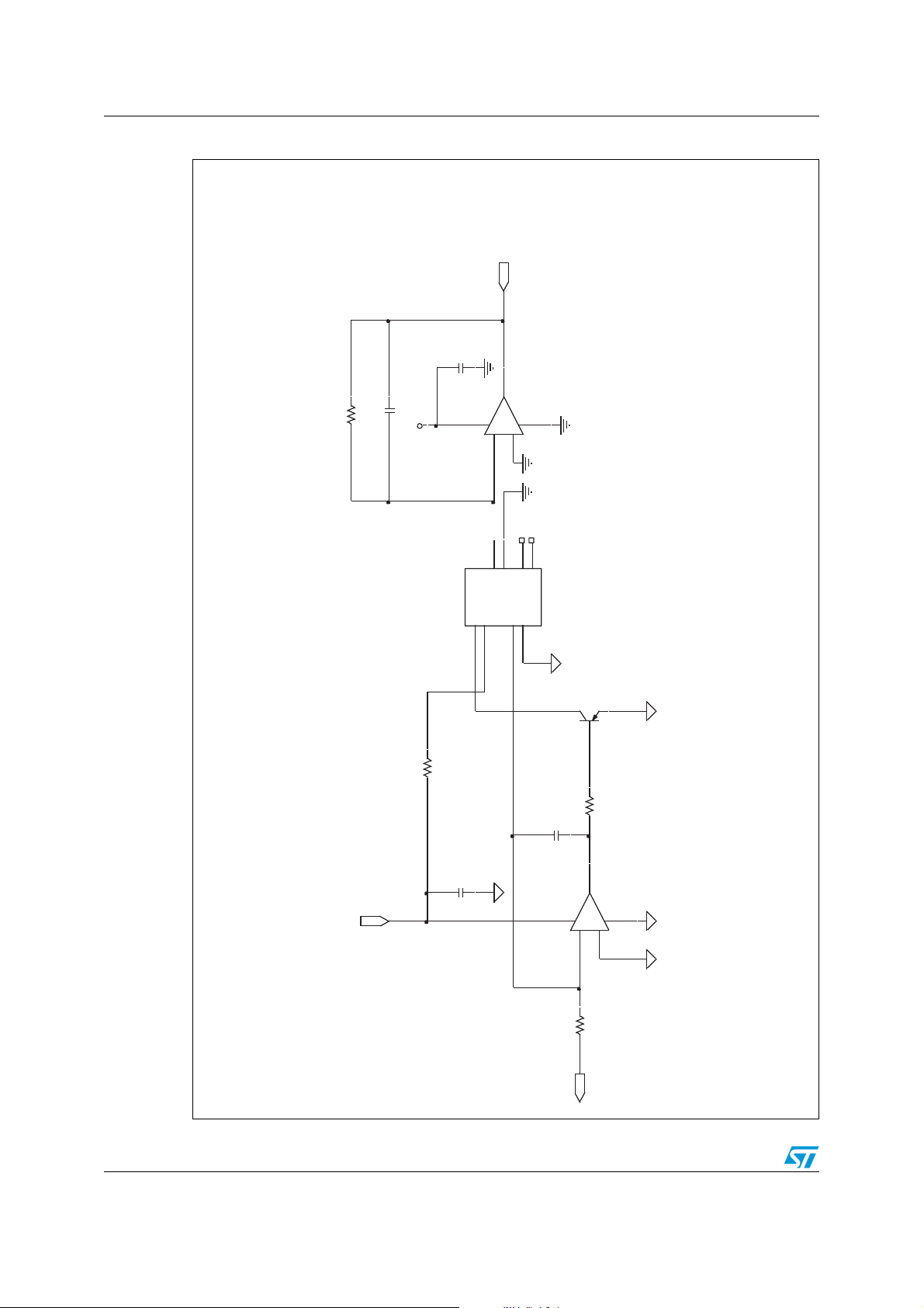
Figure 5. V-bus sensing
ADC_BU S_VOLTAGE
100n 50V
C76
1
R131
59k 1%
150p 25V
C74
3V3
U13A3
TS27 2
+
-
4 8
3
2
6
5
7
NC8NC
PD2 A
PD2 K
LED K1LED A2PD1 K
U21
R130
120
C69
100n 50V
5Visol
PD1 A
HCNR200-300
4
3
Q10
2STN2340
1k 1%
R129
C71
100n 50V
1
U13A2
TS27 2
+
-
4 8
3
2
4/12 Doc ID 022334 Rev 2
R128
86.6k 1%
Vbus_SENS
AM10196v1

STEVAL-ISV003V1 Schematics
Figure 6. 5 V isolated
DCDC L5
NMV1505SAC
Vcc15V
Vcc 15V
Gnd
5 V
0
1
2
5
7
5Visol
C55
100n 15V
Figure 7. PV voltage sensing section
R100
1k
ADC_PAN EL_VOLTAGE
IC11
1
OUT1
In1-2OUT2
3
In1+
Vcc-4In2+
TSV992
Vcc+
In2-
C56
100n 25V
5Vcc
C84
100n
8
7
6
5
R101
10k 0.1%
R103
3.3k 1%
VIN_SEN S_PV
C53
1u 25V
R102
10k 0.1%
AM10197V1
C85
10n
AM10198V1
Doc ID 022334 Rev 2 5/12

Schematics STEVAL-ISV003V1
Figure 8. DC/AC topology: mixed-frequency inverter
0.02/0.5W
Q2
Q4
STB42N65M5
OUT AC 2
STB42N65M5
SENS LE G2
R14
D6
STPS3L40S
R21
27/0.25W
LOW FREQUENCYHIGH FREQUENCY
D10
R2
3.3/0.25W
Low f PW M High Side 2
6A
Q1
600V
STB42N65M5
STPSC606
D11
D8
R23
D15
STPS3L40S
27/0.25W
R5
3.3/0.25W
Low f PW M Low Side 2
STPSC606
D34
R11
Q3
STB42N65M5
0.02/0.5W
DRAIN MO S FE T HIGH 1 DRAIN MO S FE T HIGH 2
OUT AC 1
R19
27/0.25W
D9
D16
R1
3.3/0.25W
R20
27/0.25W
D14
SENS LE G1
D17
R4
3.3/0.25W
High f PWM High Side 1
R3
15M 1%
C9
C11
22uF, 450V
22uF,450V
C10
C8
22uF, 450V
22uF, 450V
6/12 Doc ID 022334 Rev 2
Vbus_S ENS
High f PWM Low Side 1
R6
100k 1%
AM10199V1

STEVAL-ISV003V1 Schematics
Figure 9. Output AC line filter
J2
CON GRID
1
V150LA20A
SC2
2
L1_sens
12
F1
FUSE 2A
NEUTRAL_sens
SC1
12
L14
I-I+
TMOV14 R14 0E
TMOV14 R14 0E
SC3
12
N.C.
C33
2.2n, 300VAC
C30
2.2n, 300VAC
R25
T1
2 3
BU10-6003R0BL
10mH
Coilcraf t
1 4
N.C.
EARTH GROUND
C29
2.2n, 300VAC
Magnetica 2196.0001
R26
C31
470nF, 275VAC
C34
2.2n, 300VAC
2W
5.6
R28
L13
Magnetica 2196.0001
OUT AC 2
Q9
AC_NEUT
1
3
RL1
2
5
R27
Vcc15V
OUT AC 1
G5LE-1A4-DC12
D29
STPS2L25U
470
2N7002
10k 1%
R29
R36
330
RELAY_GRID
10uF 25V
C36
AM10200V1
Doc ID 022334 Rev 2 7/12

Schematics STEVAL-ISV003V1
Figure 10. Output current sensor
5Vcc
IC1
1
Vs(+)
OUT
2
3
C35
100n
R30
Iout_sens
1k 1%
C37
22n
AM10201V1
I+
I-
5
PRI Iin
4
PRI Iout
HONEY WELL
CSLW6B5
GND (-)
Figure 11. AC line current sensing
R88
10K
Vcc+
In2-
5Vcc
100nF
C79
8
7
6
5
R94
560
R96
1.1k
AC_Line current
AM10202V1
R90
R92
10K 0.1%
Iout_s ens
AC LINE CURRENT SENSOR
4k7 0.1%
IC9
1
OUT1
In1-2OUT2
3
In1+
Vcc-4In2+
TSV992
8/12 Doc ID 022334 Rev 2

STEVAL-ISV003V1 Schematics
Figure 12. VOUT sensing section
AC_Line v oltage
100nF, 16V
C72
1k, 1%
R74
C67
100nF, 16V
1
U13A1
TS272
-
+
R69
6.81k, 1%
5Vcc
4 8
10nF, 16V
2
3
C75
C68
19.4V
20k,1%
10uF, 25V
R76
6.81k, 1%
R73
180k, 1%
1nF, 50V
C70
10k, 1%
R72
6
7
5Vcc
R79
10k,1%
R84
T2
4
1
20k,1%
R86
PULSE 020-5384.0
L1_sens
NEUTRAL_sens
AM10203V1
Doc ID 022334 Rev 2 9/12

Schematics STEVAL-ISV003V1
Figure 13. 32 bit MCU-STM32F electrical schematic
-
-
D4
D10
D9D7D8
D12
D5
D6
D11
D[0..15]
KEY-LEFT
KEY-RIGH T
KEY-UP
FSMC_NE4
USER_BUTTON
20
PF921PF8
19
PF7
PF618PF515PF414PF313PF212PF111PF0
A0
PF0
10
68
PE1467PE1366PE1265PE1164PE10
PE15
PE7
63
PE960PE859PE758PE65PE54PE43PE32PE21PE1
PE2
PE3
PE1
PE1
PE2
PE3
142
PG0
PG7 KEY-CENTER
PG8 USER-BUTTON
124
PG9
PG893PG792PG691PG590PG489PG388PG2
PG0
87
22
56
57
PG0
PG1
PF1555PF1454PF1353PF1250PF1149PF10
PG12 FSMC_NE4
PG14 KEY-LEFT
PG15 KEY-UP
PG13 KEY-RIGH T
126
129
132
128
127
125
PG14
PG11
PG15
PG13
PG12
PG10
STM32F103ZET6
PA7
PA8
PA9
PA10
PA11
PA12
PA3
PA440PA541PA6
PA0-WKUP34PA135PA2
U20
43
36
37
42
100
PA7 SPI1_MOSI
PA1 RELAY-GRI D
TIM1_CH1_LEG2
PA0 TIM2_CH1
PA2 TIM5_CH3
PA3 TIM5_CH4
PWM1
PA2
PA3
SCLK (DAC)
DATA IN (DAC)
RELAY_GRID
PB046PB147PB2
PA13
PA14
PB5
PB3
PB4
PA15
48
110
101
103
104
105
102
PA13 JTAG
PA10
PWM4
PA10
TMS/SWDIO KEY-CENTER
136
109
135
133
134
BOOT1PB2
PA14 JTAG
PA15 JTAG
PB6 USART1_TX
PB0 TIM3_CH3
PB5
PB1 TIM8_CH3N
TDI
TRST
TDO/SWO
TCK/ SWC LK
PB1
PWM2
PB5
R104
10k
3V3
GND
123
J12
JUMPER_3
PB15
PC026PC127PC228PC3
PB14
PB8
PB9
PB10
PB7
PB1273PB13
PB11
PB6
76
74
70
75
69
139
140
137
PB7 USART1_RX
PB12 ENABLE (DAC)
PB11 SYNC (D AC)
PB10 LDAC (DAC)
TIM4_C H3 _LEG 1
TIM1_C H1 N
TX_0
RX_0
LDAC (DAC)
ENABLE (DAC)
SYNC (D AC)
PB13
PWM3
GND
3V3
2
3
1
J13
CON3
PC6
PC8
PC10
PC5
PC7
PC9
PC4
97
99
44
29
96
98
45
111
PC0 ADC123_IN 10
PC1 ADC123_IN 11
PC2 ADC123_IN 12
PC3 ADC123_IN 13
PC4 ADC12_IN 14
PC6 TIM8_CH1
PC5 ADC12_IN 15
PC8 TIM8 CH3
PC7 TIM8_CH2
PC9 TIM8 CH4
A0_DAC
PC5
PC9
PC7
PC8
PC6
AC_Line volt age
AC_Line current
ADC_BUS_VOLTAGE
ADC_PANEL_VOLTAGE
ADC_PANEL_CU RRENT
PC15 OSC32_OUT
12
Y1
32.768Khz 472-0887
PC14 OSC32_IN
BOOT0
PC11
PC12
PC13-ANTI_TAMP7PC14-OSC32_IN8PC15-OSC32_OUT
NOT CONNECTED
9
106
138
112
113
PC12
PC13
PC13
PC12
A1_DAC
R107 10k
R106 0
C91
10pF
GND
C90
10pF
GND
D0
D1PD15
PE0
PD14
PE0
86
141
PE0
PD1485PD15
OSC_IN23OSC_OUT24NRST
OSCIN
R115
Y2
12
8Mhz
C92
22pF
GND
GND
3
2
J14
D14PD9
D3
D15
PD10
79
81
80
82
PD10
PD12
PD11
PD13
OSCOUT
390
C9322pF
GND
1
JUMPER_3
D2PD0
KEY-DOWN
FSMC_NOE
FSMC_NWE
PD1
PD8 D13
PD4 FSMC-NOE
PD3 KEY-DOW N
PD5 FSMC-NWE
78
114
116
118
119
122
123
117
115
PD877PD9
PD0
PD2
PD4
PD5
PD6
PD7
PD3
PD1
3V3
VBAT
6
VREF+
32
VREF-
31
VSS_A
30
VDD_A
33
VDD_11
72
VDD_10
108
VDD_9
144
VDD_8
39
VDD_7
17
VDD_6
52
VDD_5
62
VDD_4
84
VDD_3
95
VDD_2
121
VDD_1
131
VSS_11
130
VSS_10
120
VSS_9
94
VSS_8
83
VSS_7
61
VSS_6
51
VSS_5
16
VSS_4
38
VSS_3
143
VSS_2
107
VSS_1
71
25
180p
GND
C94
RESET#
10k
R118
3V3
3V3
GND
C98
10nF
R121
47
GND
GND
3V3
3V3
GND
3V3
RESET
100nF
100nF
100nF
100nF
100nF
100nF
180p
180p
180p
180p
180p
180p
3V3
L16
C119
10uF
BLM41PG600SN1L
GND
GND
C118
10nF
VDDA
100nF
C112
C111
C110
C109
C108
C107
C106
C105
C104
C103
C102
C101
C124
100nF
C123
3V3
GND
3V3
GND
GND
GNDGND
GND
GND
GND
100nF
C122
C121
100nF
C120
100nF
180p
C117
180p
GNDGNDGND
C116
180p
C115
180p
C114
GND GND
C113
180p
105 0
10/12 Doc ID 022334 Rev 2
AM10204V1

STEVAL-ISV003V1 Revision history
2 Revision history
Table 1. Document revision history
Date Revision Changes
07-Oct-2011 1 Initial release.
11-Oct-2011 2 Minor text changes on cover page.
Doc ID 022334 Rev 2 11/12

STEVAL-ISV003V1
Please Read Carefully:
Information in this document is provided solely in connection with ST products. STMicroelectronics NV and its subsidiaries (“ST”) reserve the
right to make changes, corrections, modifications or improvements, to this document, and the products and services described herein at any
time, without notice.
All ST products are sold pursuant to ST’s terms and conditions of sale.
Purchasers are solely responsible for the choice, selection and use of the ST products and services described herein, and ST assumes no
liability whatsoever relating to the choice, selection or use of the ST products and services described herein.
No license, express or implied, by estoppel or otherwise, to any intellectual property rights is granted under this document. If any part of this
document refers to any third party products or services it shall not be deemed a license grant by ST for the use of such third party products
or services, or any intellectual property contained therein or considered as a warranty covering the use in any manner whatsoever of such
third party products or services or any intellectual property contained therein.
UNLESS OTHERWISE SET FORTH IN ST’S TERMS AND CONDITIONS OF SALE ST DISCLAIMS ANY EXPRESS OR IMPLIED
WARRANTY WITH RESPECT TO THE USE AND/OR SALE OF ST PRODUCTS INCLUDING WITHOUT LIMITATION IMPLIED
WARRANTIES OF MERCHANTABILITY, FITNESS FOR A PARTICULAR PURPOSE (AND THEIR EQUIVALENTS UNDER THE LAWS
OF ANY JURISDICTION), OR INFRINGEMENT OF ANY PATENT, COPYRIGHT OR OTHER INTELLECTUAL PROPERTY RIGHT.
UNLESS EXPRESSLY APPROVED IN WRITING BY TWO AUTHORIZED ST REPRESENTATIVES, ST PRODUCTS ARE NOT
RECOMMENDED, AUTHORIZED OR WARRANTED FOR USE IN MILITARY, AIR CRAFT, SPACE, LIFE SAVING, OR LIFE SUSTAINING
APPLICATIONS, NOR IN PRODUCTS OR SYSTEMS WHERE FAILURE OR MALFUNCTION MAY RESULT IN PERSONAL INJURY,
DEATH, OR SEVERE PROPERTY OR ENVIRONMENTAL DAMAGE. ST PRODUCTS WHICH ARE NOT SPECIFIED AS "AUTOMOTIVE
GRADE" MAY ONLY BE USED IN AUTOMOTIVE APPLICATIONS AT USER’S OWN RISK.
Resale of ST products with provisions different from the statements and/or technical features set forth in this document shall immediately void
any warranty granted by ST for the ST product or service described herein and shall not create or extend in any manner whatsoever, any
liability of ST.
ST and the ST logo are trademarks or registered trademarks of ST in various countries.
Information in this document supersedes and replaces all information previously supplied.
The ST logo is a registered trademark of STMicroelectronics. All other names are the property of their respective owners.
© 2011 STMicroelectronics - All rights reserved
Australia - Belgium - Brazil - Canada - China - Czech Republic - Finland - France - Germany - Hong Kong - India - Israel - Italy - Japan -
STMicroelectronics group of companies
Malaysia - Malta - Morocco - Philippines - Singapore - Spain - Sweden - Switzerland - United Kingdom - United States of America
www.st.com
12/12 Doc ID 022334 Rev 2
 Loading...