

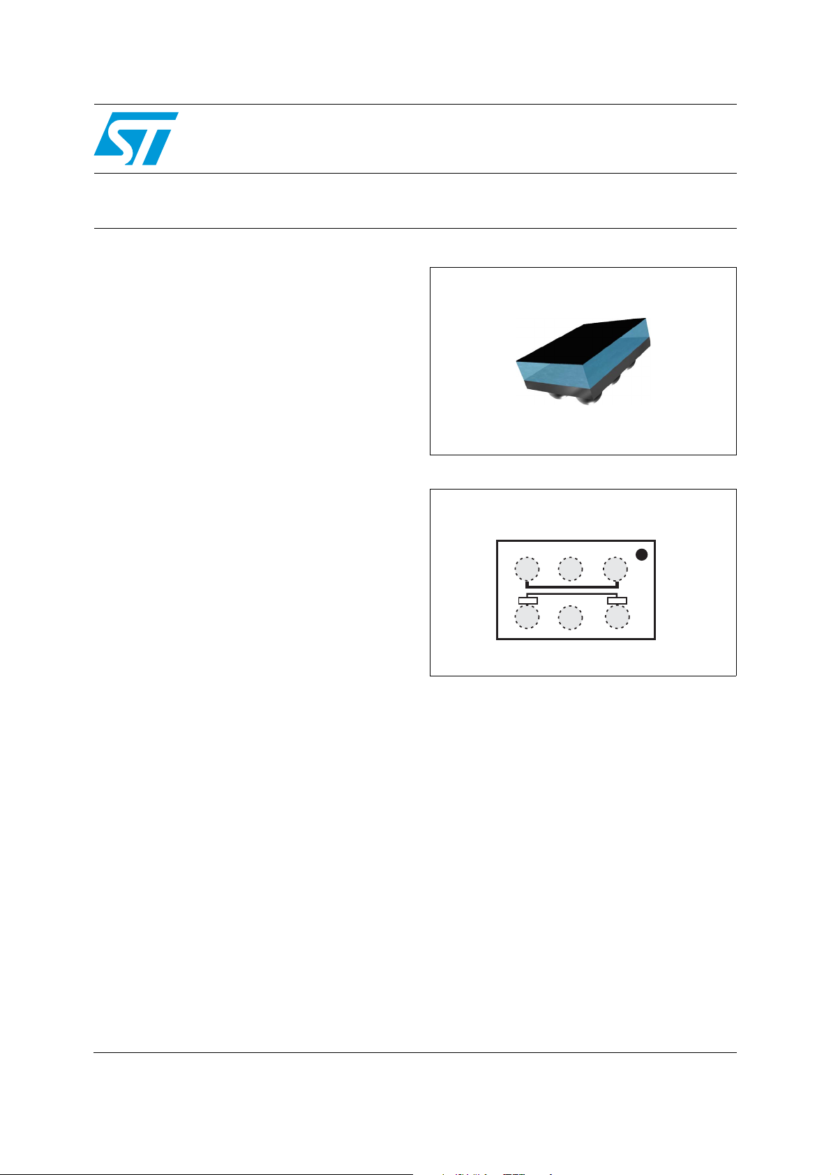
Wide band directional coupler with ISO port
Features
■ 50 Ω nominal input / output impedance
■ Wide operating frequency range
(824 MHz to 2025 MHz)
■ Low Insertion Loss (< 0.2 dB)
■ 34 dB typical coupling factor
■ High directivity (typical 25 dB)
■ High ESD robustness
(IEC 61000-4-2 Level 4)
■ Flip-Chip package
■ Small footprint: 1700 x 1200 µm
CPL-WB-01C2
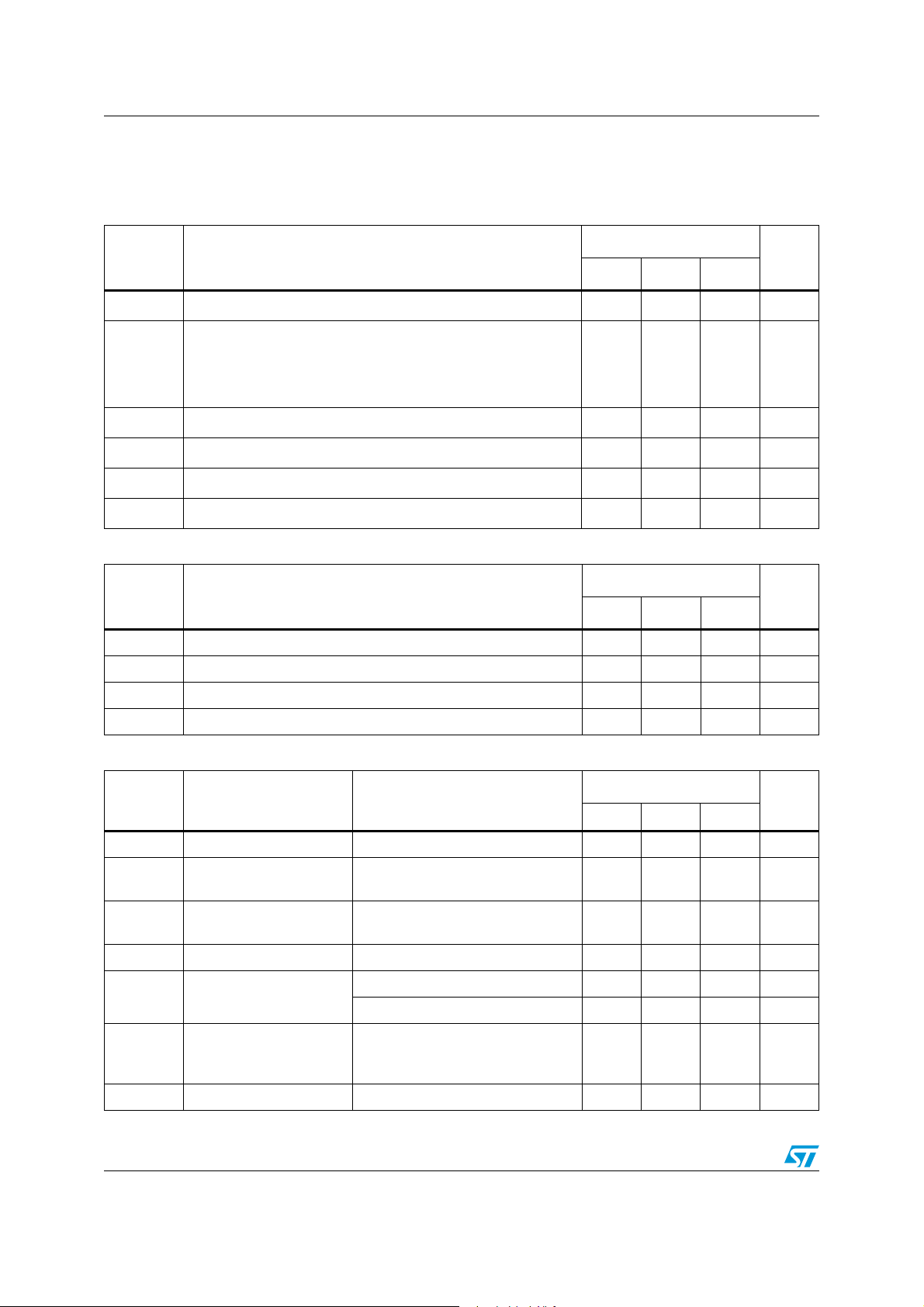
Figure 1. Pin configuration (top view)
Benefits
■ Very low profile (< 690 µm thickness)
■ Lead-free package
■ High RF performance
■ RF module size reduction
Applications
■ Quad band power amplifier module
■ Quad band front end module
■ GSM / WCDMA / TD-SCDMA mobile phone
123
RF
GND
OUT
ATN. ATN.
ISO
GND
CPLD
RF
IN
A
B
Description
The CPL-WB-01C2 is a wide band directional
coupler designed to measure RF antenna output
power in GSM / TD-SCDMA applications. This
CPL has been customized for wide band
operating frequencies (EGSM and CELL, PCS,
DCS, TD-SCDMA) with less than 0.2 dB insertion
losses in the transmit bandwidth (824 MHz to
2025 MHz).
The CPL-WB-01C2 has been designed using
STMicroelectronics IPD (integrated passive
device) technology on non conductive glass
substrate to optimize RF performance. The device
is delivered 100% tested in tape and reel.
January 2010 Doc ID 15366 Rev 3 1/8
www.st.com
8
Characteristics CPL-WB-01C2
1 Characteristics
Table 1. Absolute maximum rating (limiting values)
Value
Symbol Parameter
Min. Typ. Max.
IN
Input Power RF
IN
P
35 dBm
ESD ratings IEC 61000-4-2 (C = 150 pF, R = 330 Ω, 10 shots
V
ESD (IEC)
V
ESD (HBM)
V
ESD (MM)
V
ESD (CDM)
T
OP
Table 2. Electrical characteristics - impedances (T
with both polarities and each condition, cumulative method)
RF
RF
IN
IN
, RF
, RF
, air discharge
OUT
, contact discharge
OUT
±15
±8
Human body model, JESD22-A114-B, All I/O 2 kV
Machine model, JESD22-A115-A, All I/O 100 V
Charge device model, JESD22-C101-C, All I/O 500 V
Operating temperature -30 +85 ºC
amb
= 25 °C)
Value
Symbol Parameter
Min. Typ. Max.
Z
OUT
Z
Z
CPLD
Z
OUT
Table 3. Electrical characteristics - RF performance (T
Nominal output impedance 50 Ω
Nominal input impedance 50 Ω
IN
Nominal coupling impedance 50 Ω
Nominal ISO impedance 50 Ω
amb
= 25 °C)
Value
Symbol Parameter Test condition
Min. Typ. Max.
T
OP
I
R
CPLD
Ripple
Operating temperature -30 +85 °C
Frequency range
f
(bandwidth)
Insertion loss in
L
bandwidth
Return loss in bandwidth From 824 MHz to 2025 MHz 15 dB
L
Coupling factor (including
attenuator)
Coupling ripple in
individual band
From 824 MHz to 2025 MHz 0.1 0.2 dB
From 824 MHz to 915 MHz 35 39 dB
From 1710 MHz to 2025 MHz 28 33 dB
(824 to 849 MHz) (880 to 915 MHz)
(1710 to 1785 MHz) (1850 to
1910 MHz)(1880 to 2025 MHz)
824 2025 MHz
0.5 dB
DIR Coupler directivity From 824 MHz to 2025 MHz 20 25 dB
Unit
kV
kV
Unit
Unit
2/8 Doc ID 15366 Rev 3
CPL-WB-01C2 Characteristics
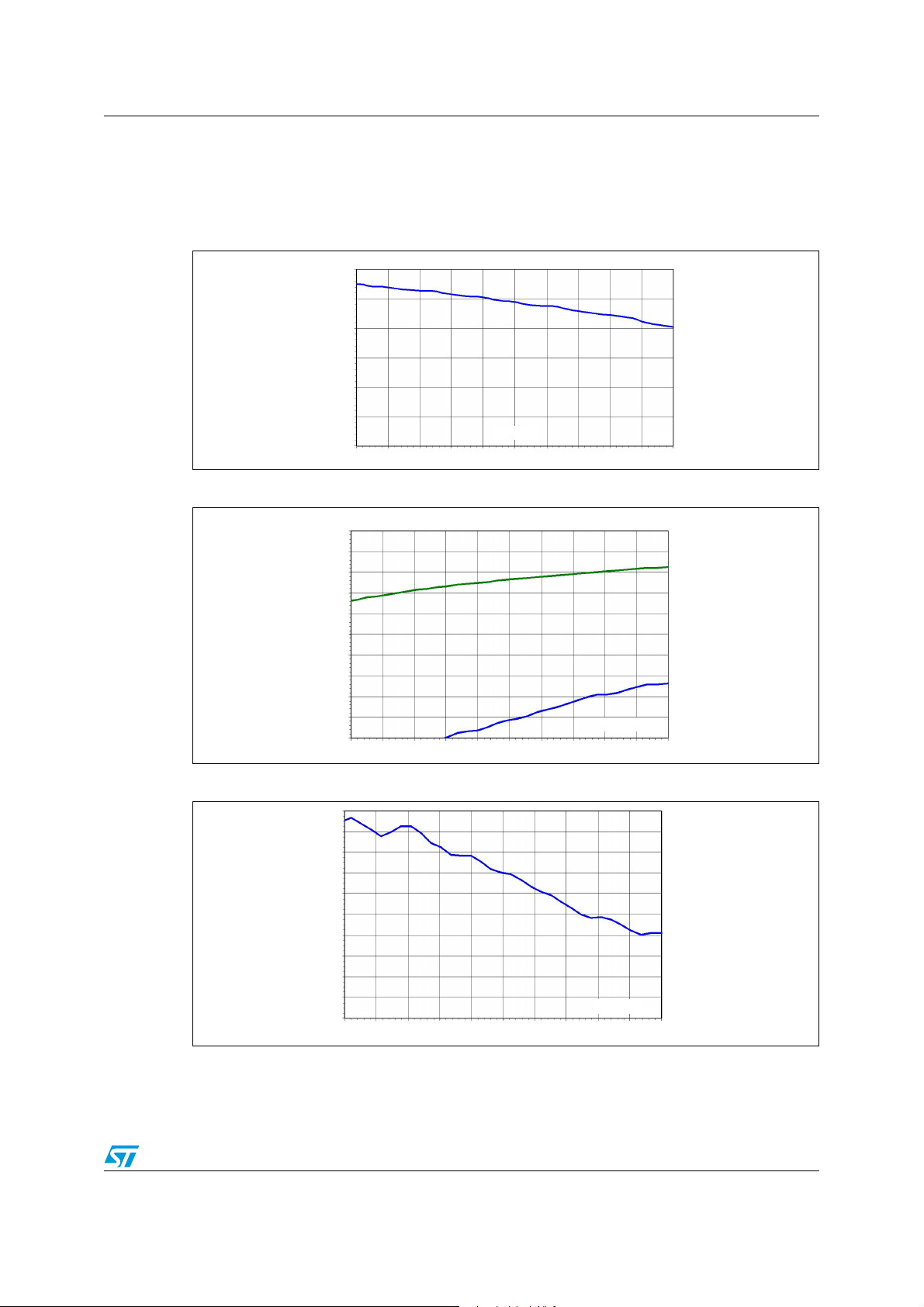
1.1 RF measurement (on reference evaluation board)
Measurements done on reference evaluation board under 50 Ω, de-embedding at
CPL-WB-01C2 bumps.
Figure 2. Insertion loss
dB
-0.0
-0.05
-0.1
-0.15
-0.2
-0.25
-0.3
Figure 3. Coupling and isolation
dB
-20
-25
-30
-35
-40
-45
-50
-55
-60
-65
-70
F (MHz)
20351901176616321497136212281093959824
F (MHz)
20351901176616321497136212281093959824
2170
2170
Figure 4. Directivity
40
38
36
34
32
30
28
26
24
22
20
F (MHz)
2170
20351901176616321497136212281093959824
Doc ID 15366 Rev 3 3/8

Reference evaluation board CPL-WB-01C2
2 Reference evaluation board
Figure 5. CPW lines (W = 850 µm with gap to gnd = 260 µm) on top layer + GND on
bottom layer
● Material: 2 layers FR4 with solder mask on top and bottom layer
● Substrate thickness: 0.8 mm
● Line lengths: 10.2 mm
● Extension values on short line measurement: 102 ps
● Through insertion loss: 0.20 dB @ 1 GHz , 0.24 dB@ 2 GHz
4/8 Doc ID 15366 Rev 3

CPL-WB-01C2 Package information
3 Package information
In order to meet environmental requirements, ST offers these devices in different grades of
ECOPACK
specifications, grade definitions and product status are available at: www.st.com
ECOPACK
®
packages, depending on their level of environmental compliance. ECOPACK®
®
is an ST trademark.
.
Figure 6. Package dimensions
650 µm
500 µm
1.200 mm ± 50 µm
1.700 mm ± 50µm
315 µm diameter
670 µm
Figure 7. Footprint Figure 8. Marking
Dot, ST logo
Copper pad Diameter:
250 µm recommended, 300 µm max
Solder stencil opening: 330 µm
Solder mask opening recommendation:
340 µm min for 300 µm copper pad diameter
xx = marking
z = manufacturing location
yww = datecode
(y = year
ww = week)
E
xyxwz
w
Doc ID 15366 Rev 3 5/8

Package information CPL-WB-01C2
Figure 9. Flip Chip tape and reel specifications
Dot identifying Pin A1 location
8 ± 0.3
ST
xxx
yww
4 ± 0.1
ST
xxx
yww
E
E
Ø 1.5 ± 0.1
ST
E
xxx
yww
1.75 ± 0.1 3.5 ± 0.1
0.73 ± 0.05
All dimensions in mm
User direction of unreeling
Note: More information is available in the application note:
AN1235: “Flip Chip: package description and recommendations for use”
4 ± 0.1
6/8 Doc ID 15366 Rev 3

CPL-WB-01C2 Ordering information
4 Ordering information
Table 4. Ordering information
Order code Marking Base qty Delivery mode
CPL-WB-01C2 RE 5000 Tape and reel
5 Revision history
Table 5. Document revision history
Date Revision Changes
15-Jan-2009 1 Initial release.
12-Oct-2009 2 Updated Table 3 value frequency range.
06-Jan-2010 3 Updated applications and description on page 1. Updated page layout.
Doc ID 15366 Rev 3 7/8

CPL-WB-01C2
Please Read Carefully:
Information in this document is provided solely in connection with ST products. STMicroelectronics NV and its subsidiaries (“ST”) reserve the
right to make changes, corrections, modifications or improvements, to this document, and the products and services described herein at any
time, without notice.
All ST products are sold pursuant to ST’s terms and conditions of sale.
Purchasers are solely responsible for the choice, selection and use of the ST products and services described herein, and ST assumes no
liability whatsoever relating to the choice, selection or use of the ST products and services described herein.
No license, express or implied, by estoppel or otherwise, to any intellectual property rights is granted under this document. If any part of this
document refers to any third party products or services it shall not be deemed a license grant by ST for the use of such third party products
or services, or any intellectual property contained therein or considered as a warranty covering the use in any manner whatsoever of such
third party products or services or any intellectual property contained therein.
UNLESS OTHERWISE SET FORTH IN ST’S TERMS AND CONDITIONS OF SALE ST DISCLAIMS ANY EXPRESS OR IMPLIED
WARRANTY WITH RESPECT TO THE USE AND/OR SALE OF ST PRODUCTS INCLUDING WITHOUT LIMITATION IMPLIED
WARRANTIES OF MERCHANTABILITY, FITNESS FOR A PARTICULAR PURPOSE (AND THEIR EQUIVALENTS UNDER THE LAWS
OF ANY JURISDICTION), OR INFRINGEMENT OF ANY PATENT, COPYRIGHT OR OTHER INTELLECTUAL PROPERTY RIGHT.
UNLESS EXPRESSLY APPROVED IN WRITING BY AN AUTHORIZED ST REPRESENTATIVE, ST PRODUCTS ARE NOT
RECOMMENDED, AUTHORIZED OR WARRANTED FOR USE IN MILITARY, AIR CRAFT, SPACE, LIFE SAVING, OR LIFE SUSTAINING
APPLICATIONS, NOR IN PRODUCTS OR SYSTEMS WHERE FAILURE OR MALFUNCTION MAY RESULT IN PERSONAL INJURY,
DEATH, OR SEVERE PROPERTY OR ENVIRONMENTAL DAMAGE. ST PRODUCTS WHICH ARE NOT SPECIFIED AS "AUTOMOTIVE
GRADE" MAY ONLY BE USED IN AUTOMOTIVE APPLICATIONS AT USER’S OWN RISK.
Resale of ST products with provisions different from the statements and/or technical features set forth in this document shall immediately void
any warranty granted by ST for the ST product or service described herein and shall not create or extend in any manner whatsoever, any
liability of ST.
ST and the ST logo are trademarks or registered trademarks of ST in various countries.
Information in this document supersedes and replaces all information previously supplied.
The ST logo is a registered trademark of STMicroelectronics. All other names are the property of their respective owners.
© 2010 STMicroelectronics - All rights reserved
STMicroelectronics group of companies
Australia - Belgium - Brazil - Canada - China - Czech Republic - Finland - France - Germany - Hong Kong - India - Israel - Italy - Japan -
Malaysia - Malta - Morocco - Philippines - Singapore - Spain - Sweden - Switzerland - United Kingdom - United States of America
www.st.com
8/8 Doc ID 15366 Rev 3
 Loading...