

Page 1
AN4041
APWlink+ microphone USB demonstration board
based on the MP34DT01, MP45DT02, or MP34DB01
Introduction
The purpose of this application note is to give a brief description of the APWlink+
microphone USB demonstration board from STMicroelectronics. This board hosts the
microcontroller STM32F107RC and either the MP45DT02 or MP34DT01 (top-port digital
microphones) and the MP34DB01 (bottom-port digital microphone). Figure 1 shows the
capability of the board to host these microphones.
These microphones are analog-to-digital transducers, in other words, they are able to sense
sound pressure and convert this signal to a digital signal using the PDM technique. The
STM32 microcontroller decodes the PDM signal coming from the microphones and streams
the audio via the USB.
This document will provide a brief description of the software that decodes the PDM signal
and also information about the hardware as well as simple steps to use the board.
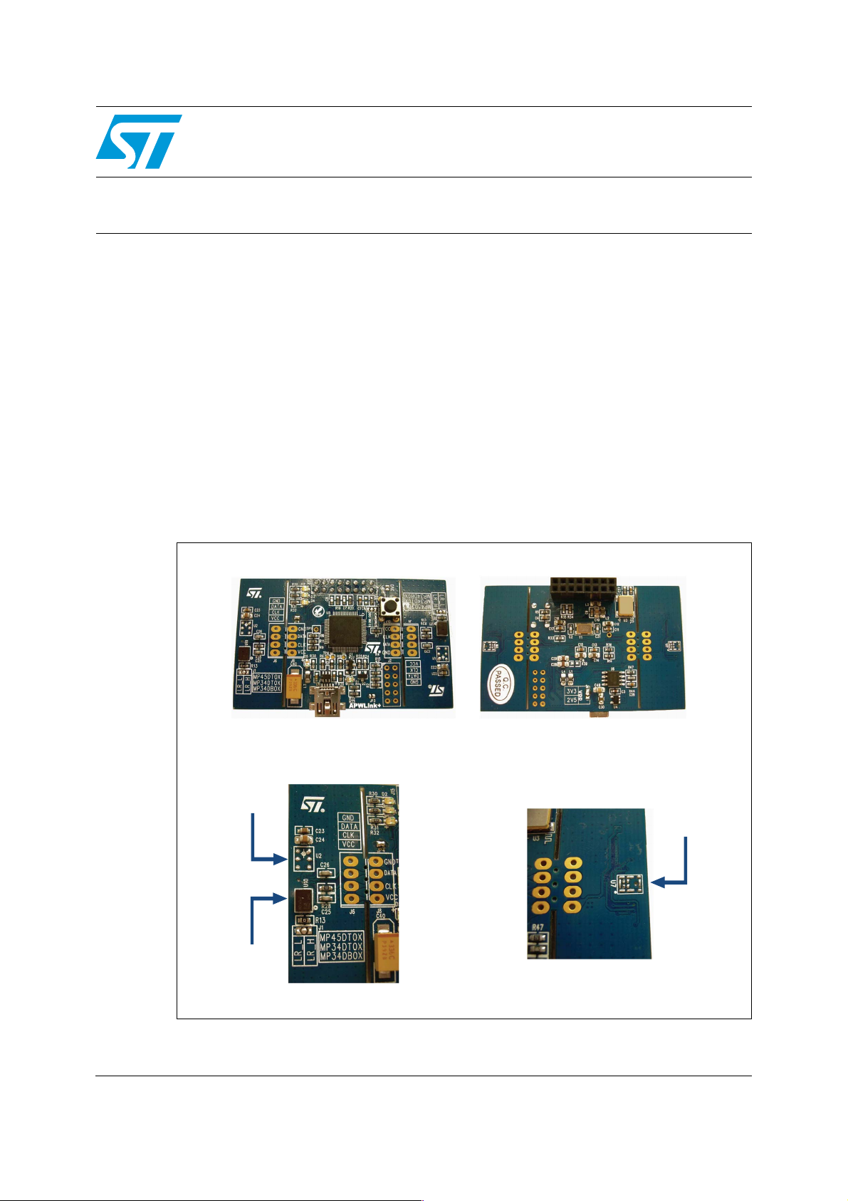
Figure 1. APWlink+ demonstration board
'VMMCPBSEWJFX
5PQ WJFX
#PUUPNWJFX
.JDSPQIPOFTFDUJPO[PPNWJFX
.1%5
.1%5
.1%#
5PQWJFX
January 2012 Doc ID 022706 Rev 1 1/12
#PUUPNWJFX
www.st.com
Page 2

Contents AN4041
Contents
1 Software description . . . . . . . . . . . . . . . . . . . . . . . . . . . . . . . . . . . . . . . . . 4
2 Hardware description . . . . . . . . . . . . . . . . . . . . . . . . . . . . . . . . . . . . . . . . 5
3 Getting started . . . . . . . . . . . . . . . . . . . . . . . . . . . . . . . . . . . . . . . . . . . . . . 7
Appendix A Schematic . . . . . . . . . . . . . . . . . . . . . . . . . . . . . . . . . . . . . . . . . . . . . . . 9
Appendix B Layout . . . . . . . . . . . . . . . . . . . . . . . . . . . . . . . . . . . . . . . . . . . . . . . . . 10
4 Revision history . . . . . . . . . . . . . . . . . . . . . . . . . . . . . . . . . . . . . . . . . . . 11
2/12 Doc ID 022706 Rev 1
Page 3

AN4041 List of figures
List of figures
Figure 1. APWlink+ demonstration board . . . . . . . . . . . . . . . . . . . . . . . . . . . . . . . . . . . . . . . . . . . . . . 1
Figure 2. DSP . . . . . . . . . . . . . . . . . . . . . . . . . . . . . . . . . . . . . . . . . . . . . . . . . . . . . . . . . . . . . . . . . . . 4
Figure 3. Microphone USB demonstration board (block diagram) . . . . . . . . . . . . . . . . . . . . . . . . . . . . 5
Figure 4. Windows message . . . . . . . . . . . . . . . . . . . . . . . . . . . . . . . . . . . . . . . . . . . . . . . . . . . . . . . . 7
Figure 5. Computer management . . . . . . . . . . . . . . . . . . . . . . . . . . . . . . . . . . . . . . . . . . . . . . . . . . . . 7
Figure 6. Recording properties . . . . . . . . . . . . . . . . . . . . . . . . . . . . . . . . . . . . . . . . . . . . . . . . . . . . . . 8
Figure 7. Schematic . . . . . . . . . . . . . . . . . . . . . . . . . . . . . . . . . . . . . . . . . . . . . . . . . . . . . . . . . . . . . . . 9
Figure 8. Board layout - top view . . . . . . . . . . . . . . . . . . . . . . . . . . . . . . . . . . . . . . . . . . . . . . . . . . . . 10
Figure 9. Board layout - bottom view . . . . . . . . . . . . . . . . . . . . . . . . . . . . . . . . . . . . . . . . . . . . . . . . . 10
Doc ID 022706 Rev 1 3/12
Page 4
Software description AN4041
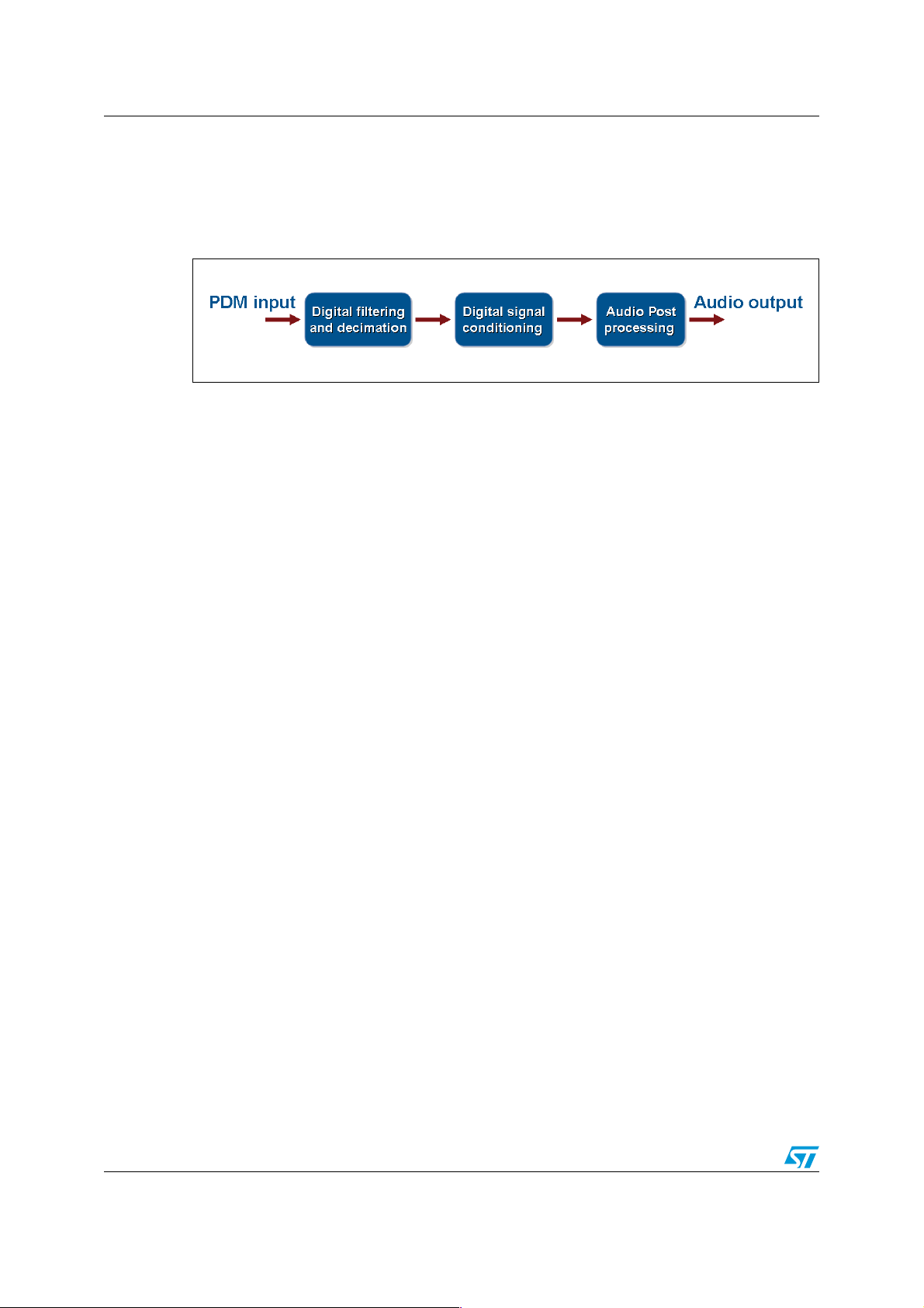
1 Software description
The digital signal processing consists of the simple flow depicted in the figure below.
Figure 2. DSP
The PDM signal from the microphone is filtered and decimated in order to obtain a sound
signal at the required frequency and resolution. The loaded firmware implements a filter
pipeline that has been designed as two filtering-decimation stages.
Assuming an input frequency of 3.072 MHz and a desired output frequency of 48 kHz, the
filter stages are configured to implement a decimation factor of 64. The final gain of the
pipeline is therefore G
signal.
For further information, please refer to application note AN3998 available on www.st.com.
= 7.8125. As a result, the output of the filter pipeline is a 16-bit PCM
1
4/12 Doc ID 022706 Rev 1
Page 5
AN4041 Hardware description
2 Hardware description
The board is a sound card automatically recognized by the PC as an audio device. The
connection is done through the USB cable which also supplies the board and then streams
the audio collected from the microphones to the PC.
Figure 3. Microphone USB demonstration board (block diagram)
APWlink+
Mic_Vdd
Vdd
Clk
L/R
J1 J5
SEL
Mic_Vdd Mic_Vdd
MIC_CK
J4
µC_Vdd
Mic_Vdd
Regulator
gnd
SEL
2.5V
Out
2.5V
MIC_DATA12
SPI_CK
Regulator
3.3V
SCL
SDA
I2C
STM32F107RC
Timer
USB I/F
3.3V
5V
BICK
LRCK
SDO12 SDO34
I2S
SPI
OSC
USB
Connector
APWlink
connector
SDO56
µC_Vdd
Out
gnd
12.288 MHz
8 MHz
D1 D2 D3 D4 D5
Mic_Vdd
Vdd
Clk
L/R
SEL
MIC_CK
Supply section
The supply section of the board is made up of two voltage regulators that step down the 5 V
of the USB connection to 3.3 V and 2.5 V. The solder jumper J4 givesthe user the possibility
to choose the desired supply voltage.The digital microphone voltage ranges are given in the
following table.
Table 1. Microphone supply voltage range
Part number Min. Typ. Max. Unit
MP45DT02 1.64 1.8 3.6 V
MP34DB01 1.64 1.8 3.6 V
MP34DT01 1.64 1.8 2.86 V
We recommend using 2.5 V to avoid supplying the microphone with a voltage that is too
high. For instance, the MP34DT01 cannot support a supply voltage of 3.3 V.
Microphone section
Regarding the microphone section, the MEMS outputs are a PDM signal, which is a highfrequency stream (1 to 3.25 MHz) of 1-bit digital samples. According to the application hints
given in the datasheets (available on www.st.com), the microphone can be used in single-
channel configuration or stereo configuration by setting the LR pin. This pin sets the validity
Doc ID 022706 Rev 1 5/12
Page 6

Hardware description AN4041
of the output data on the high level of the clock or on the low level, refer to the following
table.
Table 2. L/R channel selection
L/R Clock low Clock high
GND Data valid High impedance
VDD High impedance Data valid
On this board the microphones are used in stereo configuration, so the two digital outputs
are shorted (Mic_DATA12, refer to the schematic) and the two MEMS LR pins must be set
one to GND and the other one to VDD. On the board, the resistors R1 and R13 have already
set the LR pin of the microphones. In order to change the MEMS polarity, the user must
unsolder these resistors and manually set the LR pin using the solder jumper J1 and J5.
Note that the PCB section mounting the MEMS microphones is detachable. This option has
been implemented in order to let the user put the microphones in the desired position (i.e.
for display applications in which the microphones are placed at the edges of the display).
Microcontroller
The STM32F107RC microcontroller simultaneously works as a PDM interface and also
supports the USB audio streaming. The board hosts two external clocks, the 12.288 MHz
and 8 MHz. The first one serves to clock an internal timer for generating both MIC_CK and
SPI_CK. The 8 MHz is the microcontroller’s external clock connected to the OSC_IN
OSC_OUT pins.
The STM32 samples the microphone’s output data by using the synchronous serial port
(SPI1). The microphone signal MIC_DATA12 is a stereophonic signal and the SPI must be
able to sample both channels. Since MIC_DATA12 is synchronous with its clock, SPI_CK
must be doubled. Summarizing, the timer generates:
-MIC_CK = 3.072 MHz
-SPI_CK = 6.144 MHz
Finally, the USB interface allows streaming the audio on the USB peripheral making this
demonstration board compatible with any laptop or desktop. This streaming capability allows
using any acoustic tool for the sound acquisition done by STMicroelectronics’ MEMS
microphones. The demonstration board also has the possibility to manage the
microcontroller registers using the I
2
is the I
S which allows exporting the audio in the most commonly used digital format. This
2
C bus. Another important STM32 peripheral that is used
allows the user to test the signal using audio testing equipment such as Audio Precision. All
these signals can be monitored on the APWlink connector.
LEDs D1-D5
The status of the board is indicated by the following LEDs:
● D1 on: USB enumeration successful
● D2 on: Firmware correctly downloaded
● D3 off: Firmware correctly downloaded
● D4: not soldered
● D5 on: Board supplied
6/12 Doc ID 022706 Rev 1
Page 7

AN4041 Getting started
3 Getting started
The demonstration board is very user-friendly and is ready to use. After connecting the
micro USB cable to the laptop or desktop, the message shown in Figure 4 below appears.
This is possible since the firmware loaded into the STM microcontroller allows the operating
system to recognize the peripheral as an audio device. The version (in this case v1.0)
indicates the firmware loaded. The version v1.0 refers to a software decimator of 48 kHz as
the sampling frequency and 64 as the decimator index.
Figure 4. Windows message
The user can also check if the USB demonstration board is recognized as an audio device
by accessing the computer management and then clicking on the device manager. The
demonstration board appears as a USB audio device in the list below.
Figure 5. Computer management
Doc ID 022706 Rev 1 7/12
Page 8
Getting started AN4041
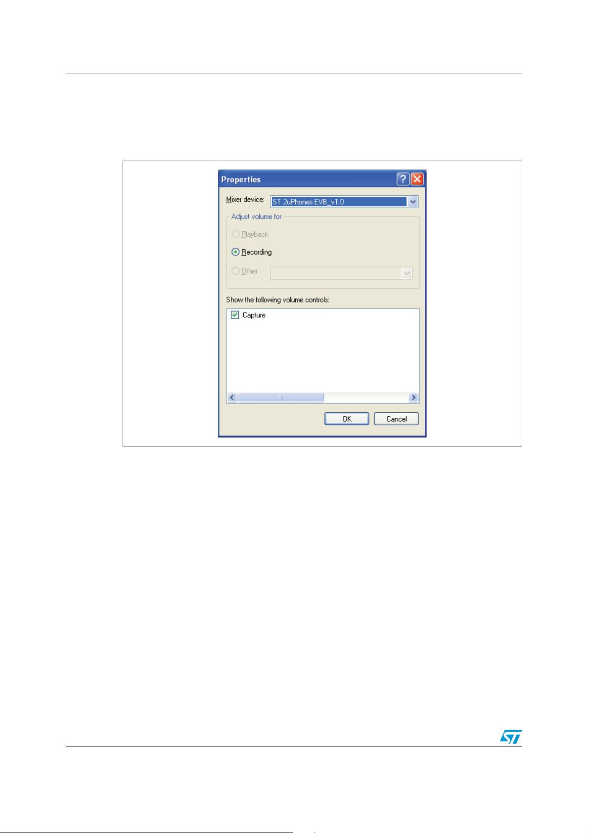
Since the firmware is able to let the operating system recognize the peripheral as an audio
device, it is possible to set the "ST 2uPhones EVB_v1.0" evaluation board as the recording
device. In this configuration, the demonstration board can be used to record the input of
general-purpose acoustic tools.
Figure 6. Recording properties
8/12 Doc ID 022706 Rev 1
Page 9

Appendix A Schematic
Figure 7. Schematic
AN4041 Schematic
Doc ID 022706 Rev 1 9/12
<Powe r Supply>
USB_DISC
Mini T ypeB
1K
VCC_USB
J7
1
VBUS
2
D-
3
D+
4
ID
5
GND
R24
1
<uCont rol le r STM32>
UC_VDD
1
1
1
R30
R31
D2
L2
820nH
BEAD
12
C10
10uF
L5
100
2
D3
LED-1
LED2
12
12
UC_VDD
1
R5
10K
2
BUT1
TACT2
2
LED3
R32
100
LED-1
NRST
D4
UC_OSC_IN
UC_OSC_OUT
C4
100nF
C9
100nF
MIC_CK
2
12
LED1
A_VDD
100
LED-1
12
12
2
1
I/O1
2
GND
3
I/O24I/O2
100nF
UC_VDD
C1
100nF
RESET
STBY
MUTE
FAIL
LED1
LED2
LED3
MIC_VDD
100
<JTAG>
UC_VDD
JUMPER_3P
A_VDD
1
MIC_CK
MIC_DATA 12
MIC_VDD
MIC_DATA 12
MIC1CK
MIC_DATA 12
SDA
3
4
MP34DB01
3
4
JTCK
NRST
JRST
U7
2
L/R
VDD
1
DATA
CLK
GND
5
U10
2
CLK
L/R
1
DATA
VDD
MIC_VDD
GND
MP34DT01
5
MIC_VDD
MIC_DATA 12
1
1
R3
R2
10K
10K
2
2
STM32_I 2S_BI CK
STM32_I2S_LRCK
JP3
JP
<Microp hone s>
J1
MIC1LR
JUMPER_3P
MIC1LR
J5
JUMPER_3P
MIC2LR
3
4
10K
12
MIC_VDD
3
2
1
MIC_VDD
3
2
1
U9
1
R4
2
JTMS
1
R15
10K
2
R13
0R0
1
2
3
1
2
R1
0R0
3
2
VDD
L/R
1
DATA
CLK
GND
5
MP34DB01
U2
GND
LR
GND
U1
GND
LR
GND
5X2_HEADER
MP45DT01
MP45DT01
MIC2CK
UC_VDD
12
34
56
78
910
J2
MIC_VDD
C24
10uF
C23
6
VDD
5
DOUT
4
CLK
C26
15pF
6
VDD
5
DOUT
4
CLK
C20
15pF
3
CLK
4
DATA
100nF
MIC_DATA 12
MIC1CK
2
1
R28
MIC_CK
100
C25
15pF
MIC_VDD
C22
10uF
C21
100nF
MIC_DATA 12
MIC2CK
2
1
R29
MIC_CK
C19
100
15pF
U11
2
MIC2LR
L/R
1
VDD
MP34DT01
MIC_VDD
GND
5
VCC_USB UC_VDDUC_VDD
1
1
R25
47k
2
USBLC6-2
C17
100nF
R23
10k
2
C
1
Q2
B
R22
36k
E
2
U8
R6
2
6
I/O1
5
VBUS
R12
2
C5
100nF
UC_VDD
1
R33
C18
10K
4.7uF
2
63
64
1
VSS_3
VDD_3
VBAT
2
PC13-TAMPER-RTC
3
PC14-OSC32_IN
4
PC15-OSC32_OUT
5
PD0_OSC_IN
6
PD1_OSC_OUT
7
NRST
8
PC0
9
PC1
10
PC2
11
PC3
12
VSSA
13
VDDA
14
PA0-WKUP
15
PA1
16
PA2
PA318VSS_419VDD_420PA4
17
UC_VDD
C11
C12
4.7uF
B
22
1
22
1
UC_VDDUC_VDD
R35
1k
61
62
PB9
PB8
1
C
R27
Q1
0R0 NC
2
E
R26
2
1
180
2
1
R8
1.5K
2
USBDM
USBDP
1
1
R34
1k
2
2
56
57
59
60
PB558PB6
PB7
BOOT0
U5
PA623PA724PC4
PA5
21
22
25
JP4
JP
SPI1_C loc k
LED-1
1
<Mangusta option> <Clock Generators>
VSS_CAP
54
55
PB3
PB4
PD2
PB128PB229PB10
27
12
MIC_DATA 12
STM32_LQFP64
12.288_CK
VSS_1
PB11
30
31
PC526PB0
TP1
D1
49
PA1450PA1551PC1052PC1153PC12
VDD_2
VSS_2
PA13
PA12
PA11
PA10
PB15
PB14
PB13
PB12
VDD_1
32
48
47
46
45
44
43
42
PA9
41
PA8
40
PC9
39
PC8
38
PC7
37
PC6
36
35
34
33
UC_VDD
C14
4.7uF
VCC_USB
C41
10nF
2
R39
0R0 NC
STM32_I2S_DATA34
STM32_I2S_BICK
STM32_I2S_LRCK
SDA
SCL
JRST
MCO
JTCK
100nF
2
R14
0R0
C13
100nF
1
C28
2.2uF
C15
1
12
UC_VDD
JTMS
USBDP
USBDM
USB_DISC
MCO
TP2
TP3
TP4
VSS_CAP
2
R36
0R0
L3
INDUCTOR2
BEAD
R38
D5
LED-1
C29
2.2uF
C16
4.7uF
STM32_I2S_MCLK
STM32_I2S_DATA12
STM32_I2S_BICK
STM32_I2S_LRCK
1
27
1
2
12
VSS_CAP
C40
33uF
U4
1
VIN
OUT
LDS3985XX
3
VINH
BYPASS
GND
2
4
1
IN
2
OUT1
3
OUT2
4
+
UC_VDD
12.288_CK
<Connectors>
MCLK
J3
JUMPER_3P
ADJ
C39
1
2
3
2
1
100nF
R37
10k
MIC_VDD
LM317LM
R47
2
1
1.6K
U3
12
34
XT_ACTIVE
3.3V
I2S_DAT_12
I2S_DAT_56
I2S_BICK
2
SCL
JP1
JP
MUTE FAIL
1
0R0
R21
2
1
C6
NS
STM32_I 2S_MCL K
12.288_CK
2
3
1
123
I2S_DAT_12
I2S_DAT_34 STM32_I2S_DATA34
I2S_BICK
I2S_LRCK
5
U6
1
UC_OSC_IN
UC_OSC_OUT
2
R20
J8
CON4
4
4
J6
CON4
2
2
2
2
C3
330nF
OUT4
OUT3
R44
1K
0R0
0R0
0R0
0R0
8
7
6
5
2
C27
100nF
1
100
R9
R7
R11
R10
2.5V
C30
4.7uF
3.3V
12
34
56
78
910
11 12
13 14
15 16
C7
10pF
MIC_CK
MIC_DATA 12
1
1
1
1
C49
1uF
12
Y1
8.000MHz
J15
MIC_VDD
STM32_I2S_DATA12
STM32_I2S_BICK
STM32_I2S_LRCK
34
UC_VDD
12
C2
18pF
C31
18pF
1
2
123
1
2
3
INDUCTOR2
12
L4
INDUCTOR2
BEAD
2
C8
10pF
3
BEAD
R19
4
4
J4
L1
I2S_DAT_34
I2S_LRCK
RESET
STBY
J10
CON4
J9
CON4
Page 10
Layout AN4041
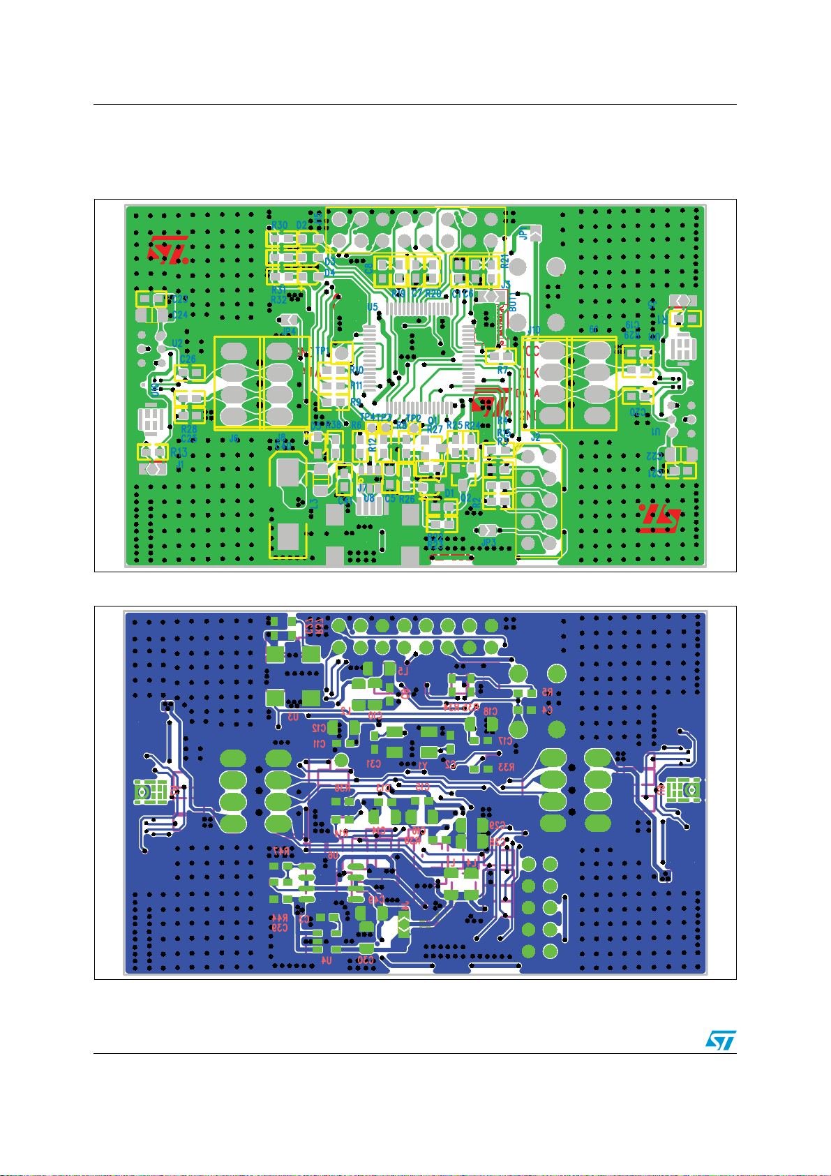
Appendix B Layout
Figure 8. Board layout - top view
Figure 9. Board layout - bottom view
10/12 Doc ID 022706 Rev 1
Page 11

AN4041 Revision history
4 Revision history
Table 3. Document revision history
Date Revision Changes
30-Jan-2012 1 Initial release.
Doc ID 022706 Rev 1 11/12
Page 12

AN4041
Please Read Carefully:
Information in this document is provided solely in connection with ST products. STMicroelectronics NV and its subsidiaries (“ST”) reserve the
right to make changes, corrections, modifications or improvements, to this document, and the products and services described herein at any
time, without notice.
All ST products are sold pursuant to ST’s terms and conditions of sale.
Purchasers are solely responsible for the choice, selection and use of the ST products and services described herein, and ST assumes no
liability whatsoever relating to the choice, selection or use of the ST products and services described herein.
No license, express or implied, by estoppel or otherwise, to any intellectual property rights is granted under this document. If any part of this
document refers to any third party products or services it shall not be deemed a license grant by ST for the use of such third party products
or services, or any intellectual property contained therein or considered as a warranty covering the use in any manner whatsoever of such
third party products or services or any intellectual property contained therein.
UNLESS OTHERWISE SET FORTH IN ST’S TERMS AND CONDITIONS OF SALE ST DISCLAIMS ANY EXPRESS OR IMPLIED
WARRANTY WITH RESPECT TO THE USE AND/OR SALE OF ST PRODUCTS INCLUDING WITHOUT LIMITATION IMPLIED
WARRANTIES OF MERCHANTABILITY, FITNESS FOR A PARTICULAR PURPOSE (AND THEIR EQUIVALENTS UNDER THE LAWS
OF ANY JURISDICTION), OR INFRINGEMENT OF ANY PATENT, COPYRIGHT OR OTHER INTELLECTUAL PROPERTY RIGHT.
UNLESS EXPRESSLY APPROVED IN WRITING BY TWO AUTHORIZED ST REPRESENTATIVES, ST PRODUCTS ARE NOT
RECOMMENDED, AUTHORIZED OR WARRANTED FOR USE IN MILITARY, AIR CRAFT, SPACE, LIFE SAVING, OR LIFE SUSTAINING
APPLICATIONS, NOR IN PRODUCTS OR SYSTEMS WHERE FAILURE OR MALFUNCTION MAY RESULT IN PERSONAL INJURY,
DEATH, OR SEVERE PROPERTY OR ENVIRONMENTAL DAMAGE. ST PRODUCTS WHICH ARE NOT SPECIFIED AS "AUTOMOTIVE
GRADE" MAY ONLY BE USED IN AUTOMOTIVE APPLICATIONS AT USER’S OWN RISK.
Resale of ST products with provisions different from the statements and/or technical features set forth in this document shall immediately void
any warranty granted by ST for the ST product or service described herein and shall not create or extend in any manner whatsoever, any
liability of ST.
ST and the ST logo are trademarks or registered trademarks of ST in various countries.
Information in this document supersedes and replaces all information previously supplied.
The ST logo is a registered trademark of STMicroelectronics. All other names are the property of their respective owners.
© 2012 STMicroelectronics - All rights reserved
STMicroelectronics group of companies
Australia - Belgium - Brazil - Canada - China - Czech Republic - Finland - France - Germany - Hong Kong - India - Israel - Italy - Japan -
Malaysia - Malta - Morocco - Philippines - Singapore - Spain - Sweden - Switzerland - United Kingdom - United States of America
www.st.com
12/12 Doc ID 022706 Rev 1
 Loading...