

Page 1

1 Introduction
The SPC56x family of devices has internal Flash used for code and data. The Nexus debug
interface can be used to program the Flash using the JTAG communication protocol through
the JTAG port. This allows programming of the internal Flash by an external tool.
This application note first addresses the JTAG and Nexus communication protocol. The
JTAG discussion includes the JTAG signals, TAP controller state machine, and the JTAG
controller. The explanation of Nexus includes the on-chip emulation (OnCE) module and the
Nexus read/write (R/W) access block.
Nexus/JTAG Flash programming supports the following products:
● SPC563Mxx
● SPC564Axx
● SPC560Dxx
● SPC560Bxx
● SPC560Cxx
● SPC560Pxx
● SPC56ELxx
AN4035
Application note
Flash programming through
Nexus/JTAG
January 2012 Doc ID 022669 Rev 1 1/41
www.st.com
Page 2

Contents AN4035
Contents
1 Introduction . . . . . . . . . . . . . . . . . . . . . . . . . . . . . . . . . . . . . . . . . . . . . . . . 1
2 JTAG . . . . . . . . . . . . . . . . . . . . . . . . . . . . . . . . . . . . . . . . . . . . . . . . . . . . . . 6
2.1 JTAG signals . . . . . . . . . . . . . . . . . . . . . . . . . . . . . . . . . . . . . . . . . . . . . . . 6
2.2 TAP controller state machine . . . . . . . . . . . . . . . . . . . . . . . . . . . . . . . . . . . 6
2.3 JTAG controller (JTAGC) . . . . . . . . . . . . . . . . . . . . . . . . . . . . . . . . . . . . . . 7
2.4 Modes of operation . . . . . . . . . . . . . . . . . . . . . . . . . . . . . . . . . . . . . . . . . . . 8
2.4.1 Reset . . . . . . . . . . . . . . . . . . . . . . . . . . . . . . . . . . . . . . . . . . . . . . . . . . . . 9
2.4.2 Test mode . . . . . . . . . . . . . . . . . . . . . . . . . . . . . . . . . . . . . . . . . . . . . . . . 9
2.5 Enabling debug of a censored device . . . . . . . . . . . . . . . . . . . . . . . . . . . 10
2.5.1 CENSOR_CTRL register . . . . . . . . . . . . . . . . . . . . . . . . . . . . . . . . . . . . 12
3 On-Chip Emulation (OnCE) . . . . . . . . . . . . . . . . . . . . . . . . . . . . . . . . . . 13
3.1 Enabling the OnCE TAP controller . . . . . . . . . . . . . . . . . . . . . . . . . . . . . . 13
3.2 OnCE register access . . . . . . . . . . . . . . . . . . . . . . . . . . . . . . . . . . . . . . . 14
3.3 OnCE command register . . . . . . . . . . . . . . . . . . . . . . . . . . . . . . . . . . . . . 14
3.3.1 Example of OnCE register write . . . . . . . . . . . . . . . . . . . . . . . . . . . . . . 17
3.3.2 Example of OnCE register read . . . . . . . . . . . . . . . . . . . . . . . . . . . . . . . 18
3.4 OnCE status register . . . . . . . . . . . . . . . . . . . . . . . . . . . . . . . . . . . . . . . . 19
3.5 Entering debug mode during reset . . . . . . . . . . . . . . . . . . . . . . . . . . . . . . 20
3.6 Enabling external debug mode and other initialization . . . . . . . . . . . . . . . 21
3.7 CPU Status and Control Scan Chain Register (CPUSCR) . . . . . . . . . . . 21
3.7.1 Instruction Register (IR) . . . . . . . . . . . . . . . . . . . . . . . . . . . . . . . . . . . . . 22
3.7.2 Control State Register (CTL) . . . . . . . . . . . . . . . . . . . . . . . . . . . . . . . . . 23
3.7.3 Program Counter Register (PC) . . . . . . . . . . . . . . . . . . . . . . . . . . . . . . . 24
3.7.4 Write-Back Bus Register (WBBRlow, WBBRhigh) . . . . . . . . . . . . . . . . . 24
3.7.5 Machine State Register (MSR) . . . . . . . . . . . . . . . . . . . . . . . . . . . . . . . 24
3.8 Single step . . . . . . . . . . . . . . . . . . . . . . . . . . . . . . . . . . . . . . . . . . . . . . . . 24
3.9 Exit from debug mode to normal execution . . . . . . . . . . . . . . . . . . . . . . . 25
3.10 GPR access . . . . . . . . . . . . . . . . . . . . . . . . . . . . . . . . . . . . . . . . . . . . . . . 25
3.11 SPR access . . . . . . . . . . . . . . . . . . . . . . . . . . . . . . . . . . . . . . . . . . . . . . . 25
3.12 OnCE memory access . . . . . . . . . . . . . . . . . . . . . . . . . . . . . . . . . . . . . . . 26
2/41 Doc ID 022669 Rev 1
Page 3

AN4035 Contents
3.13 Breakpoints . . . . . . . . . . . . . . . . . . . . . . . . . . . . . . . . . . . . . . . . . . . . . . . 26
3.13.1 Software breakpoints . . . . . . . . . . . . . . . . . . . . . . . . . . . . . . . . . . . . . . . 27
3.13.2 Instruction address hardware breakpoints . . . . . . . . . . . . . . . . . . . . . . . 27
4 Nexus Read/Write access block . . . . . . . . . . . . . . . . . . . . . . . . . . . . . . 28
4.1 Nexus register access . . . . . . . . . . . . . . . . . . . . . . . . . . . . . . . . . . . . . . . 30
4.2 Single memory write access . . . . . . . . . . . . . . . . . . . . . . . . . . . . . . . . . . 32
4.3 Burst block memory write access . . . . . . . . . . . . . . . . . . . . . . . . . . . . . . . 32
4.4 Single memory read access . . . . . . . . . . . . . . . . . . . . . . . . . . . . . . . . . . . 33
4.5 Burst block memory read access . . . . . . . . . . . . . . . . . . . . . . . . . . . . . . . 34
5 System initialization . . . . . . . . . . . . . . . . . . . . . . . . . . . . . . . . . . . . . . . . 35
5.1 Internal SRAM initialization . . . . . . . . . . . . . . . . . . . . . . . . . . . . . . . . . . . 35
5.2 Setting up the memory management unit . . . . . . . . . . . . . . . . . . . . . . . . 35
6 Creating the Flash programming tool . . . . . . . . . . . . . . . . . . . . . . . . . . 36
6.1 Flash programming drivers . . . . . . . . . . . . . . . . . . . . . . . . . . . . . . . . . . . . 36
6.2 Tool requirements . . . . . . . . . . . . . . . . . . . . . . . . . . . . . . . . . . . . . . . . . . . 36
6.2.1 Debug and driver initialization . . . . . . . . . . . . . . . . . . . . . . . . . . . . . . . . 36
6.2.2 FlashInit . . . . . . . . . . . . . . . . . . . . . . . . . . . . . . . . . . . . . . . . . . . . . . . . . 37
6.2.3 SetLock . . . . . . . . . . . . . . . . . . . . . . . . . . . . . . . . . . . . . . . . . . . . . . . . . 37
6.2.4 FlashErase . . . . . . . . . . . . . . . . . . . . . . . . . . . . . . . . . . . . . . . . . . . . . . . 38
6.2.5 FlashProgram . . . . . . . . . . . . . . . . . . . . . . . . . . . . . . . . . . . . . . . . . . . . 38
6.2.6 Using other drivers . . . . . . . . . . . . . . . . . . . . . . . . . . . . . . . . . . . . . . . . . 39
6.3 Functional division of the external tool . . . . . . . . . . . . . . . . . . . . . . . . . . . 40
Doc ID 022669 Rev 1 3/41
Page 4

List of tables AN4035
List of tables
Table 1. JTAG signal properties . . . . . . . . . . . . . . . . . . . . . . . . . . . . . . . . . . . . . . . . . . . . . . . . . . . . . 6
Table 2. JTAG instructions . . . . . . . . . . . . . . . . . . . . . . . . . . . . . . . . . . . . . . . . . . . . . . . . . . . . . . . . 10
Table 3. OnCE command register bit definitions . . . . . . . . . . . . . . . . . . . . . . . . . . . . . . . . . . . . . . . 15
Table 4. e200z0 OnCE Register Addressing . . . . . . . . . . . . . . . . . . . . . . . . . . . . . . . . . . . . . . . . . . 16
Table 5. RWCS field description. . . . . . . . . . . . . . . . . . . . . . . . . . . . . . . . . . . . . . . . . . . . . . . . . . . . 28
Table 6. Read/Write access status bit encoding. . . . . . . . . . . . . . . . . . . . . . . . . . . . . . . . . . . . . . . . 29
Table 7. JTAG Data Register (DR) . . . . . . . . . . . . . . . . . . . . . . . . . . . . . . . . . . . . . . . . . . . . . . . . . . 31
Table 8. Nexus register index . . . . . . . . . . . . . . . . . . . . . . . . . . . . . . . . . . . . . . . . . . . . . . . . . . . . . . 31
4/41 Doc ID 022669 Rev 1
Page 5

AN4035 List of figures
List of figures
Figure 1. TAP controller finite state machine . . . . . . . . . . . . . . . . . . . . . . . . . . . . . . . . . . . . . . . . . . . . 7
Figure 2. JTAG controller block diagram . . . . . . . . . . . . . . . . . . . . . . . . . . . . . . . . . . . . . . . . . . . . . . . 8
Figure 3. Enabling JTAG/Nexus port access on a censored device . . . . . . . . . . . . . . . . . . . . . . . . . 11
Figure 4. e200z OnCE block diagram . . . . . . . . . . . . . . . . . . . . . . . . . . . . . . . . . . . . . . . . . . . . . . . . 13
Figure 5. Steps for enabling the OnCE TAP controller . . . . . . . . . . . . . . . . . . . . . . . . . . . . . . . . . . . 14
Figure 6. Signal transitions for enabling the OnCE TAP controller . . . . . . . . . . . . . . . . . . . . . . . . . . 14
Figure 7. OnCE command register . . . . . . . . . . . . . . . . . . . . . . . . . . . . . . . . . . . . . . . . . . . . . . . . . . 15
Figure 8. DBCR0 register. . . . . . . . . . . . . . . . . . . . . . . . . . . . . . . . . . . . . . . . . . . . . . . . . . . . . . . . . . 17
Figure 9. Signal transitions for writing OCMD to select a write to DBCR0. . . . . . . . . . . . . . . . . . . . . 18
Figure 10. Signal transitions for writing DBCR0. . . . . . . . . . . . . . . . . . . . . . . . . . . . . . . . . . . . . . . . . . 18
Figure 11. Signal transitions for writing OCMD to select a read from DBCR0 . . . . . . . . . . . . . . . . . . . 19
Figure 12. Signal transitions for reading DBCR0 . . . . . . . . . . . . . . . . . . . . . . . . . . . . . . . . . . . . . . . . . 19
Figure 13. OnCE status register . . . . . . . . . . . . . . . . . . . . . . . . . . . . . . . . . . . . . . . . . . . . . . . . . . . . . 20
Figure 14. Signal transitions of reading the OnCE status register . . . . . . . . . . . . . . . . . . . . . . . . . . . . 20
Figure 15. OnCE control register . . . . . . . . . . . . . . . . . . . . . . . . . . . . . . . . . . . . . . . . . . . . . . . . . . . . . 20
Figure 16. Debug Status Register (DBSR) . . . . . . . . . . . . . . . . . . . . . . . . . . . . . . . . . . . . . . . . . . . . . 21
Figure 17. CPU status and control scan chain register . . . . . . . . . . . . . . . . . . . . . . . . . . . . . . . . . . . . 22
Figure 18. Control State Register (CTL) . . . . . . . . . . . . . . . . . . . . . . . . . . . . . . . . . . . . . . . . . . . . . . . 23
Figure 19. Read/Write Access Control/Status Register (RWCS). . . . . . . . . . . . . . . . . . . . . . . . . . . . . 28
Figure 20. Read/Write access data register (RWD). . . . . . . . . . . . . . . . . . . . . . . . . . . . . . . . . . . . . . . 30
Figure 21. Read/Write access address register (RWA) . . . . . . . . . . . . . . . . . . . . . . . . . . . . . . . . . . . 30
Doc ID 022669 Rev 1 5/41
Page 6

JTAG AN4035
2 JTAG
JTAG is a serial communication protocol developed by the Joint Test Access Group.
Originally developed for boundary scan, JTAG is also used for communication with the
Nexus debug interface (NDI) on the SPC560x devices.
2.1 JTAG signals
The JTAG port of the SPC56x devices consists of the TCK, TDI, TDO, TMS and JCOMP
pins. TDI, TDO, TMS, and TCK are compliant with the IEEE 1149.1-2001 standard and are
shared with the NDI through the test access port (TAP) interface. See Ta bl e 1 for signal
properties.
Table 1. JTAG signal properties
Name I/O Function
TCK I Test Clock
TDI I Test Data In
TDO O Test Data Out
TMS I Test Mode Select
JCOMP I JTAG Compliancy
The JCOMP pin assertion allows to put the JTAGC in reset state.
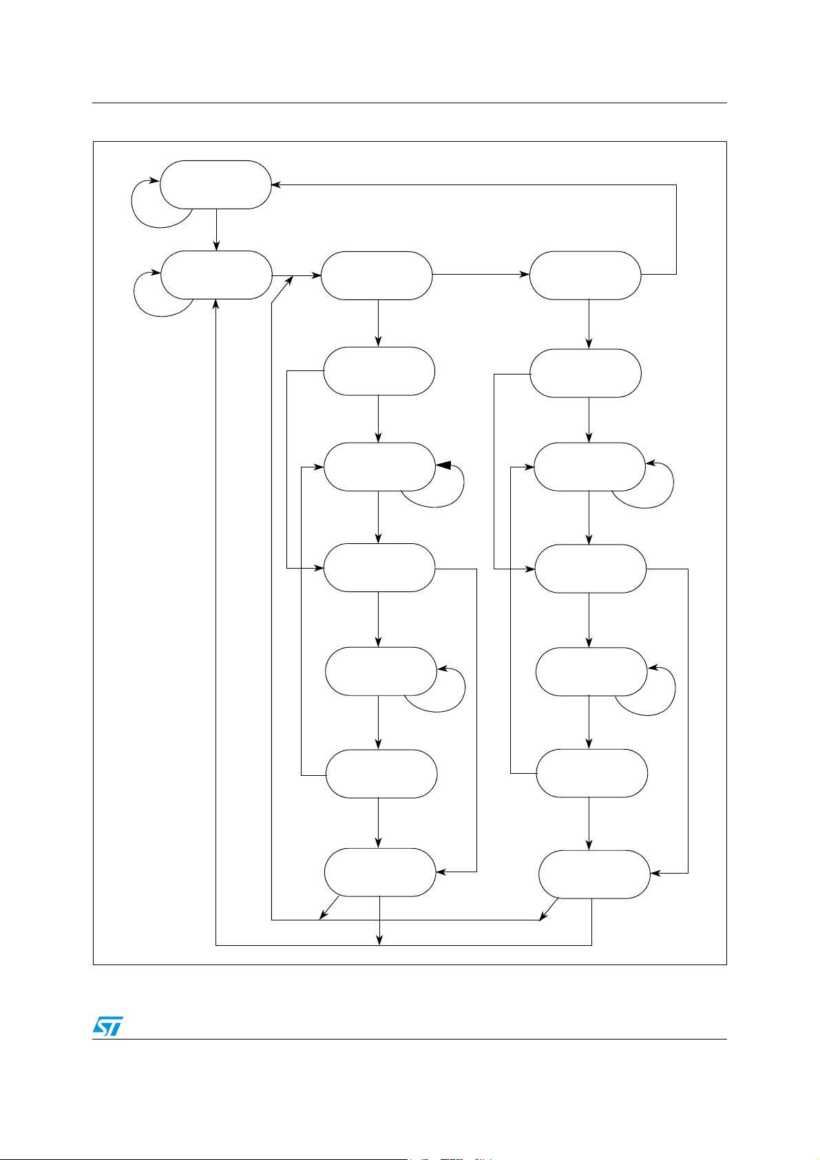
2.2 TAP controller state machine
The TAP controller state machine controls the JTAG logic. The TAP controller state machine
is a 16-state finite state machine (FSM) as shown in Figure 1. The TCK and TMS signals
control transition between states of the FSM. These two signals control whether an
instruction register scan or data register scan is performed. Both the TDI and TMS inputs
are sampled on the rising edge of TCK while the TDO output changes on the falling edge of
TCK. The value shown next to each state of the state machine in Figure 2 is the value of
TMS required on the rising edge of TCK to transition to the connected state. Five rising
edges of TCK with TMS at logic 1 guarantee entry into the TEST LOGIC RESET state.
6/41 Doc ID 022669 Rev 1
Page 7
AN4035 JTAG
Figure 1. TAP controller finite state machine
7(67/2*,&
5(6(7
5817(67,'/ (
6(/(&7'56&$1
&$3785('5
6+ ,)7'5
(;,7' 5
6(/(&7,56&$1
&$3785(,5
6+ ,)7,5
(;,7,5
3$8 6 ('5
(;,7'5
83'$7('5
Doc ID 022669 Rev 1 7/41
3$86(,5
(;,7,5
83'$7(,5
Page 8
JTAG AN4035
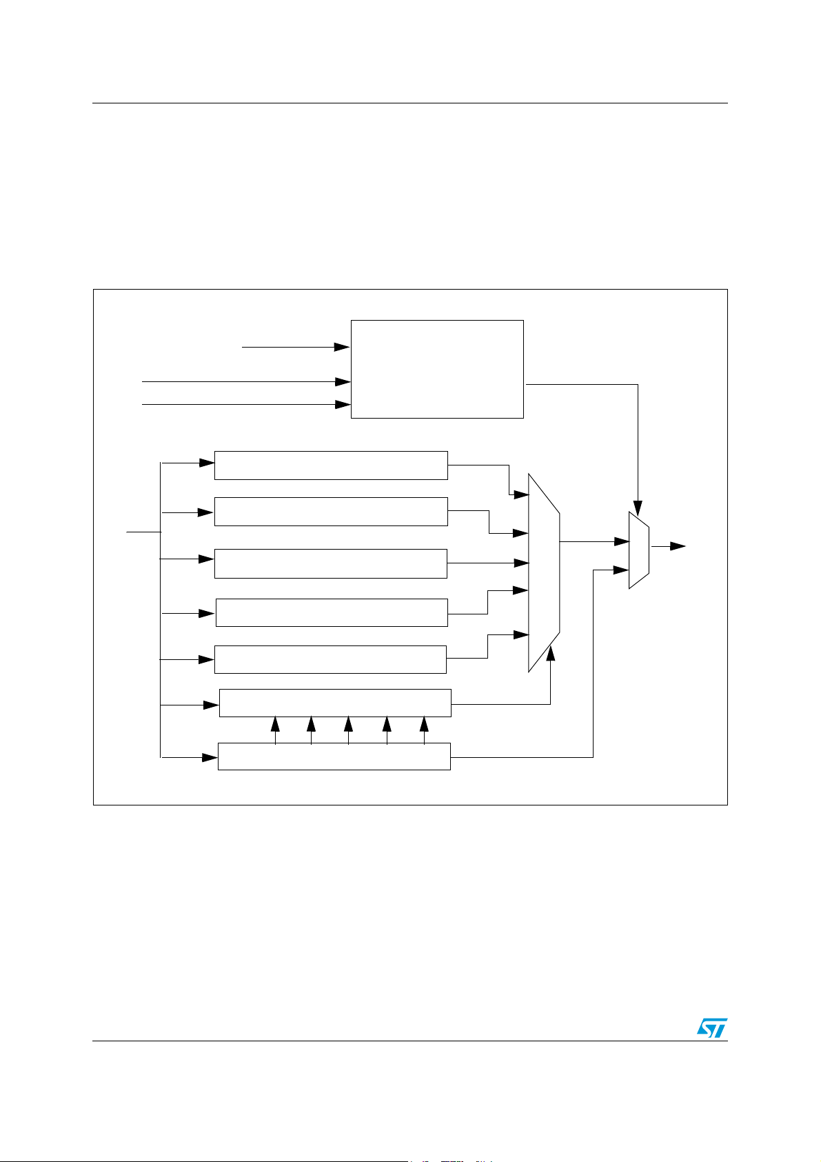
2.3 JTAG controller (JTAGC)
The JTAGC provides the means to test chip functionality and connectivity while remaining
transparent to system logic when not in TEST mode. Testing is performed via a boundary
scan technique, as defined in the IEEE 1149.1-2001 standard. In addition, instructions can
be executed in order to allow the Test Access Port (TAP) to be shared with other modules on
the MCU. All data input to and output from the JTAGC is communicated in serial format. A
block diagram of the JTAGC is shown in Figure 3.
Figure 2. JTAG controller block diagram
JCOMP
Test Access Port (TAP)
TMS
TCK
Controller
TDI
.
.
.
.
.
.
.
.
1-Bit Bypass Register
32-Bit Device Identification Register
Boundary Scan Register
TEST_CTRL Register
CENSOR_CTRL Register
5-Bit TAP Instruction Decoder
5-Bit TAP Instruction Register
2.4 Modes of operation
TDO
Access to the JTAGC data registers is done by loading the instruction register with any of
the JTAGC instructions while the JTAGC is enabled. Instructions are shifted in via the selectIR-scan path and loaded in the update-IR state. At this point, all data register access is
performed via the select-DR-scan path.
The select-DR-scan path is used to read or write the register data by shifting in the data
(LSB first) during the shift-DR state. When reading a register, the register value is loaded
into the shifter during the capture-DR state. When writing a register, the value is loaded from
8/41 Doc ID 022669 Rev 1
Page 9

AN4035 JTAG
the shifter to the register during the update-DR state. When reading a register, there is no
requirement to shift out the entire register contents. Shifting can be terminated after fetching
the required number of bits.
2.4.1 Reset
The JTAGC is placed in reset when the TAP controller state machine is in the TEST-LOGICRESET state.
The TEST-LOGIC-RESET state is entered upon the assertion of the power-on reset signal,
negation of JCOMP, or through TAP controller state machine transitions controlled by TMS.
Asserting power-on reset or negating JCOMP results in asynchronous entry into the reset
state. While in reset, the following actions occur:
● The TAP controller is forced into the test-logic-reset state, thereby disabling the test
logic and allowing normal operation of the on-chip system logic to continue unhindered.
● The instruction register is loaded with the IDCODE instruction.
In addition, execution of EXTEST instruction results in assertion of the internal system reset.
2.4.2 Test mode
Several TEST modes are supported, as well as a bypass mode and they are entered using
the following instructions:
● EXTEST
● SAMPLE
● SAMPLE/PRELOAD
Each instruction defines the set of data registers that can operate and interact with the onchip system logic while the instruction is current. Only one test data register path is enabled
to shift data between TDI and TDO for each instruction.
Following the test modes available:
1. BYPASS mode
When no test operation is required, the BYPASS instruction can be loaded to place the
JTAGC into bypass mode. While in bypass mode, the single-bit bypass shift register is
used to provide a minimum-length serial path to shift data between TDI and TDO.
2. TAP Sharing Mode
There are three selectable auxiliary TAP controllers that share the TAP with the JTAGC.
Selectable TAP controllers include:
- Nexus port controller (NPC)
- On Chip Emulator (ONCE) controller
- TCU controller
The instructions required to grant ownership of the TAP to the auxiliary TAP controllers are
ACCESS_AUX_TAP_NPC, ACCESS_AUX_TAP_ONCE, ACCESS_AUX_TAP_TCU.
Instruction opcodes for each instruction are shown in Tab l e 2.
When the access instruction for an auxiliary TAP is loaded, control of the JTAG pins is
transferred to the selected TAP controller. Any data input via TDI and TMS is passed to the
selected TAP controller, and any TDO output from the selected TAP controller is sent back to
the JTAGC to be output on the pins. The JTAGC regains control of the JTAG port during the
UPDATE-DR state if the PAUSE-DR state was entered. Auxiliary TAP controllers are held in
RUN-TEST/IDLE while they are inactive.
Doc ID 022669 Rev 1 9/41
Page 10

JTAG AN4035
Table 2. JTAG instructions
Instruction Code[4:0] Instruction summary
IDCODE 00001
SAMPLE/PRELOAD 00010
SAMPLE 00011
EXTEST 00100
ACCESS_AUX_TAP_TCU 10000
ACCESS_AUX_TAP_ONCE 10001
ACCESS_AUX_TAP_NPC 10010
Reserved 10010 -
BYPASS 11111
Selects device identification
register for shift
Selects boundary scan register
for shifting, sampling, and
preloading without disturbing
functional operation
Selects boundary scan register
for shifting and sampling without
disturbing functional operation
Selects boundary scan register
while applying preloaded values
to
output pins and asserting
functional reset
Grants the TCU ownership of
the TAP
Grants the PLATFORM
ownership of the TAP
Grants the Nexus port controller
(NPC) ownership of the TAP
Selects bypass register for data
operations
00101
Factory Debug Reserved
Reserved All other codes
00110
01010
2.5 Enabling debug of a censored device
When a device is in a censored state, the debug port (JTAG/Nexus) is disabled and only
JTAG BSDL commands can be used. Access to the Nexus/JTAG clients on a censored
device requires inputting the proper password into the JTAG Censorship Control Register
during reset.
When the debug port is enabled on a censored device, it is enabled only until the next reset.
Figure 3 shows the logic that enables access to Nexus clients in a censored device using
the JTAG port.
Intended for factory debug only
Decoded to select bypass
register
10/41 Doc ID 022669 Rev 1
Page 11
AN4035 JTAG
Figure 3. Enabling JTAG/Nexus port access on a censored device
Censored Flash Array
64-bit Password
Compare
JTAG Port Controller
CENSOR_CTRL register
Enable/disable
Other Nexus Clients
•eDMA
• e200z3 processor
.
.
.
Nexus client
TAP controller
64-bit Password
Debug/Calibration Tool
Access
The steps to enable the debug port on a censored device are as follows:
1. After the RSTOUT pin has is negated, hold the device in system reset state using a
debugger or other tool.
2. While the device is being held in system reset state shift the 64-bit password into the
CENSOR_CTRL register (via the JTAG port using the JTAG
ENABLE_CENSOR_CTRL instruction. The JTAG serial password is compared against
the serial boot flash password from the flash shadow block.
3. If there is a match the Nexus client TAP controller enters normal operation mode and
the DISNEX flag in the SIU_CCR register is negated (for the SPC56xB and SPC56xP
families the flag NXEN in the SSCM_STATUS register is negated) indicating Nexus is
enabled. Upon negation of reset the debug / calibration tool is able to access the device
via NEXUS port and JTAG. If the JTAG serial password does not match the serial boot
flash password or the serial boot flash password is an illegal password then the debug /
calibration tool is not able to access the device. After the debug port is enabled, the tool
can access the censored device and can erase and reprogram the shadow flash block
in order to uncensor the device.
Doc ID 022669 Rev 1 11/41
Page 12

JTAG AN4035
Note: If the shadow flash block is erased without reprogramming a new valid password before a
reset, it contains an illegal password and the debug port is inaccessible.
4. Subsequent resets clear the JTAG censor password register and the Nexus client TAP
controller holds in reset again. Therefore, the tool must resend the JTAG serial
password, as described above, in order to enable the Nexus client TAP controller again.
2.5.1 CENSOR_CTRL register
The CENSOR_CTRL register is an shift register path from TDI to TDO selected when the
ENABLE_CENSOR_CTRL instruction is active. The CENSOR_CTRL register transfers its
value to a parallel hold register on the rising edge of TCK when the TAP controller state
machine is in the Update-DR state. The parallel hold register bits CENSOR_CTRL
correspond directly to the JTAGC output control internal signals jtag_censor_ctrl. The
jtag_censor_ctrl signals are used to control chip dependent censorship features. Once the
ENABLE_CENSOR_CTRL instruction is executed, jtag_censor_ctrl remains valid until a
JTAGC reset occurs.
12/41 Doc ID 022669 Rev 1
Page 13
AN4035 On-Chip Emulation (OnCE)
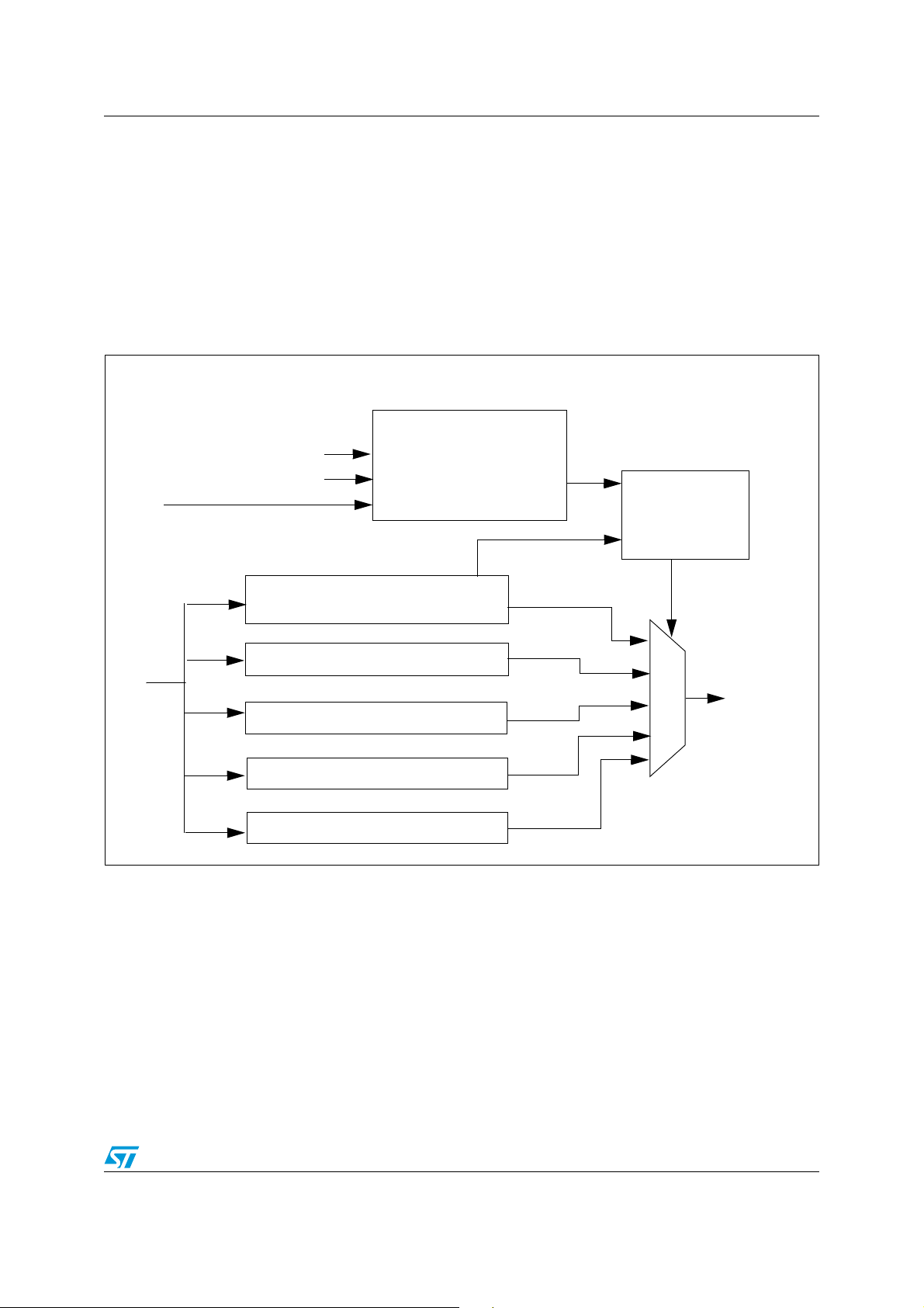
3 On-Chip Emulation (OnCE)
From
JTAGC
TCK
TDI
All of the SPC56x devices possess a OnCE module for debug control of the Power
Architecture
including run-time control, register access, and memory access to all memory-mapped
regions including on-chip peripherals, as well as providing access to the Nexus2 & Nexus3
configuration registers. The OnCE module is controlled by the JTAG signals through the
OnCE TAP controller.
Figure 4. e200z OnCE block diagram
e200z0_TRST
{
e200z0_TMS
.
.
.
.
®
e200 core. The OnCE logic provides Nexus class 1 static debug capability
Test Access Port (TAP)
Controller
TDO Mux
Control
TAP Instruction Register
(OnCE OCMD)
Bypass Register
e200z0_TDO
External Data Register
(to JTAGC)
.
.
OnCE Mapped Debug Registers
Auxiliary Data Register
3.1 Enabling the OnCE TAP controller
Control of the OnCE module is obtained through the OnCE TAP controller. To enable the
OnCE TAP controller, the JTAGC must have control of the TAP and the
ACCESS_AUX_TAP_ONCE (0b10001) opcode must be loaded into the 5-bit JTAGC
instruction register with the JCOMP signal set to a logic 1.
The JTAGC instruction register is loaded by scanning in the appropriate bits on the TDI pin,
least significant bit (LSB) first, while in the SHIFT-IR state of the TAP controller state
machine. The last bit is shifted in with TMS set to a logical 1 causing transition from the
SHIFT-IR state to the EXIT1-IR state. Table 3-1 shows the steps required to enable the
OnCE TAP controller, assuming the TAP controller state machine is initially in the RUN-
Doc ID 022669 Rev 1 13/41
Page 14
On-Chip Emulation (OnCE) AN4035
TEST/IDLE state. The state machine is returned to the RUN-TEST/IDLE state when the
write is complete.
Figure 5. Steps for enabling the OnCE TAP controller
TCK tick TMS TDI Resulting state
1 1 X SELECT-DR-SCAN
2 1 X SELECT-IR-SCAN
3 0 X CAPTURE-IR
40XSHIFT-IR
501SHIFT-IR
600SHIFT-IR
700SHIFT-IR
800SHIFT-IR
911SHIFT-IR
10 1 X UPDATE-IR
11 0 X RUN-TEST/IDLE
Figure 6. Signal transitions for enabling the OnCE TAP controller
3.2 OnCE register access
The OnCE module provides several registers for static debug support. The OnCE command
register (OCMD) is a special register and acts as the IR for the TAP controller state machine
and is used to access other OnCE resources.
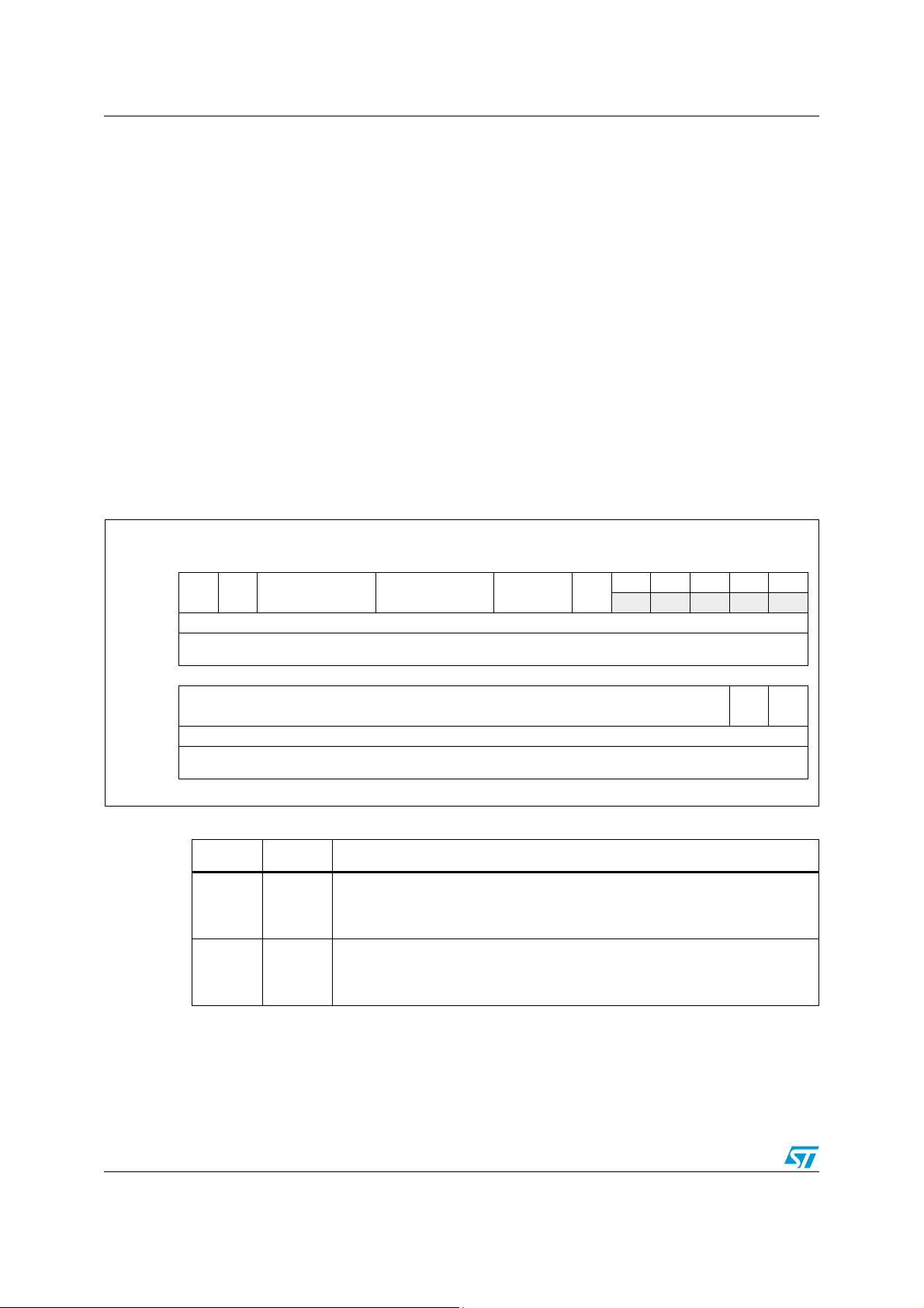
3.3 OnCE command register
The OnCE command register (OCMD) is a 10-bit shift register that receives its serial data
from the TDI pin and acts as the IR register of the TAP controller state machine. The OCMD
is updated when the TAP controller enters the UPDATE-IR state. It contains fields for
14/41 Doc ID 022669 Rev 1
Page 15

AN4035 On-Chip Emulation (OnCE)
controlling access to a resource, as well as controlling single step operations and exit from
debug mode. Figure 7 shows the register definition for the OnCE command register.
Figure 7. OnCE command register
0123456789
R
W
Reset:0000011011
R/W GO EX RS[0:6]
Ta bl e 3 provides bit definitions for the once command register.
Reset - 0b10_0000_0010 on assertion of JCOMP, during power on reset, or while in the
TEST LOGIC RESET state.
Table 3. OnCE command register bit definitions
Bit(s) Name Description
0R/W
Read/Write Command Bit
The R/W bit specifies the direction of data transfer. The table below describes the options
defined by the R/W bit.
0 Write the data associated with the command into the register specified by RS[0:6]
1 Read the data contained in the register specified by RS[0:6]
Note: The R/W bit is ignored for read-only or write-only registers. In addition, it is ignored for
all bypass operations. When performing writes, most registers are sampled in the Capture-DR
state into a 32-bit shift register, and subsequently shifted out on TDO during the first 32 clocks
of Shift-DR.
Go Command Bit
0 Inactive (no action taken)
1 Execute instruction in IR
If the GO bit is set, the chip executes the instruction which resides in the IR register in the
CPUSCR. To execute the instruction, the processor leaves debug mode, executes the
instruction, and if the EX bit is cleared, returns to debug mode immediately after executing the
1GO
instruction. The processor goes on to normal operation if the EX bit is set, and no other debug
request source is asserted. The GO command is executed only if the operation is a read/write
to CPUSCR or a read/write to “No Register Selected”. Otherwise the GO bit is ignored.The
processor leaves debug mode after the TAP controller Update-DR state is entered.
On a GO+NoExit operation, returning to debug mode is treated as a debug event, thus
exceptions such as machine checks and interrupts may take priority and prevent execution of
the intended instruction. Debug firmware should mask these exceptions as appropriate. The
OSR[ERR] bit indicates such an occurrence.
Doc ID 022669 Rev 1 15/41
Page 16

On-Chip Emulation (OnCE) AN4035
Table 3. OnCE command register bit definitions (continued)
Bit(s) Name Description
0 Remain in debug mode
1 Leave debug mode
If the EX bit is set, the processor leaves debug mode and resume normal operation until
another debug request is generated. The Exit command is executed only if the Go command
is issued, and the operation is a read/write to CPUSCR or a read/write to “No Register
2EX
3-9 RS
Selected”. Otherwise the EX bit is ignored.
The processor leaves debug mode after the TAP controller Update-DR state is entered. Note
that if the DR bit in the OnCE control register is set or remains set, or if a bit in the DBSR is set,
or if a bit in the DBSR is set and DBCR0[EDM]=1 (external debug mode is enabled), then the
processor may return to debug mode without execution of an instruction, even though the EX
bit was set.
Register Select
The Register Select bits define which register is source (destination) for the read (write)
operation. Attempted writes to read-only registers are ignored.
Ta bl e 4 shows the OnCE register addresses. Access to the registers CPUSCR, DAC1-2,
DBCNT, DBCR0-3, DBSR, and IAC1-4 require that the external debug mode bit,
DBCR0[EDM], be set to a logical 1. Only the DBCR0[EDM] is accessible in the DBCR0
register prior to that bit being set. Setting DBCR0[EDM] enables external debug mode and
disables software updates to debug registers. The CPU should be placed in debug mode via
the OCR[DR] bit prior to setting the DBCR0[EDM] bit.
Table 4. e200z0 OnCE Register Addressing
RS[0:6] Register selected
000 0000 Reserved
000 0001 Reserved
000 0010 JTAG ID (read-only)
000 0011-000 1111 Reserved
001 0000 CPU Scan Register (CPUSCR)
001 0001 No Register Selected (Bypass)
001 0010 OnCE Control Register (OCR)
001 0011-001 1111 Reserved
010 0000 Instruction Address Compare 1 (IAC1)
010 0001 Instruction Address Compare 2 (IAC2)
010 0010 Instruction Address Compare 3 (IAC3)
010 0011 Instruction Address Compare 4 (IAC4)
010 0100 Data Address Compare 1 (DAC1)
010 0101 Data Address Compare 2 (DAC2)
010 0110 Data Value Compare 1 (DVC1)
010 0111 Data Value Compare 2 (DVC2)
16/41 Doc ID 022669 Rev 1
Page 17

AN4035 On-Chip Emulation (OnCE)
Table 4. e200z0 OnCE Register Addressing (continued)
RS[0:6] Register selected
010 1000 -010 1011 Reserved
010 1100 Debug Counter Register (DBCNT)
010 1101 Debug PCFIFO (PCFIFO) (read-only)
010 1110 -010 1111 Reserved
011 0000 Debug Status Register (DBSR)
011 0001 Debug Control Register 0 (DBCR0)
011 0010 Debug Control Register 1 (DBCR1)
011 0011 Debug Control Register 2 (DBCR2)
011 0100-101 1111 Reserved
111 0000 -111 1001 General Purpose register selects [0:9]
111 1010 Cache Debug Access Control Register (CDACNTL)
111 1011 Cache Debug Access Data Register (CDADATA)
111 1100 Nexus3-Access
111 1101 Reserved
111 1110 Enable_OnCE
111 1111 Bypass
3.3.1 Example of OnCE register write
OnCE registers can be written by selecting the register using the RS[0:6] field and clearing
the R/W bit in the OnCE command register (OCMD). This requires a scan through the IR
path of the TAP controller state machine to write the OCMD and a scan through the DR path
of the TAP controller state machine to write the selected register. As mentioned above, the
external debug mode bit, DBCR0[EDM], must be set to a logical 1 to allow access to most of
the OnCE registers. Therefore, writing the DCBR0 register to set the EDM bit is used as an
example of a writing a OnCE register. Figure 8 shows the register definition of DBCR0.
Figure 8. DBCR0 register
01234 5 6 7 8 9101112131415
R
EDM IDM RST ICMP BRT IRPT TRAP IAC1 IAC2 IAC3 IAC4 DAC1 DAC2
W
Reset00000 0 0 0 0 0 0 00000
16 17 18 19 20 21 22 23 24 25 26 27 28 29 30 31
R
W
Reset00000 0 0 0 0 0 0 00000
0000
RET
DEVT1 DEVT2 DCNT1 DCNT2 CRPT CRET
0000
The example of writing DBCR0 is divided into two parts: writing OCMD to select a write to
DBCR0, and writing the value 0x80000000 to DBCR0. All data are scanned in least
significant bit first.
FT
Doc ID 022669 Rev 1 17/41
Page 18

On-Chip Emulation (OnCE) AN4035
Figure 9 shows writing the value 0b00_0011_0001 to OCMD through the IR path to select a
write to DBCR0 assuming the TAP controller state machine is initially in the RUNTEST/IDLE state. The state machine is returned to the RUN-TEST/IDLE state when the
write is complete.
Figure 9. Signal transitions for writing OCMD to select a write to DBCR0
'DWD VW D UWV RQ
WKLVFORFNHGJH
Figure 10 shows writing the value 0x80000000 to DBCR0 through the DR path to set the
EDM bit assuming the TAP controller state machine is initially in the RUN-TEST/IDLE state.
The state machine is returned to the RUN-TEST/IDLE state when the write is complete.
Figure 10. Signal transitions for writing DBCR0
3.3.2 Example of OnCE register read
OnCE registers can be read by selecting the register using the RS[0:6] field and setting the
R/W bit in the OnCE command register (OCMD). This requires a scan through the IR path of
the TAP controller state machine to write the OCMD and a scan through the DR path of the
TAP controller state machine to read the selected register. This read example reads DBCR0
after the EDM bit is set.
Figure 11 shows writing the value 0b10_0011_0001 to OCMD through the IR path to select
a read from DBCR0 assuming the TAP controller state machine is initially in the RUNTEST/IDLE state. The state machine is returned to the RUN-TEST/IDLE state when the
write is complete.
18/41 Doc ID 022669 Rev 1
Page 19

AN4035 On-Chip Emulation (OnCE)
Figure 11. Signal transitions for writing OCMD to select a read from DBCR0
Figure 12 shows reading the value 0x80000000 from DBCR0 through the DR path
assuming the TAP controller state machine is initially in the RUN-TEST/IDLE state. The
state machine is returned to the RUN-TEST/IDLE state when the read is complete.
Figure 12. Signal transitions for reading DBCR0
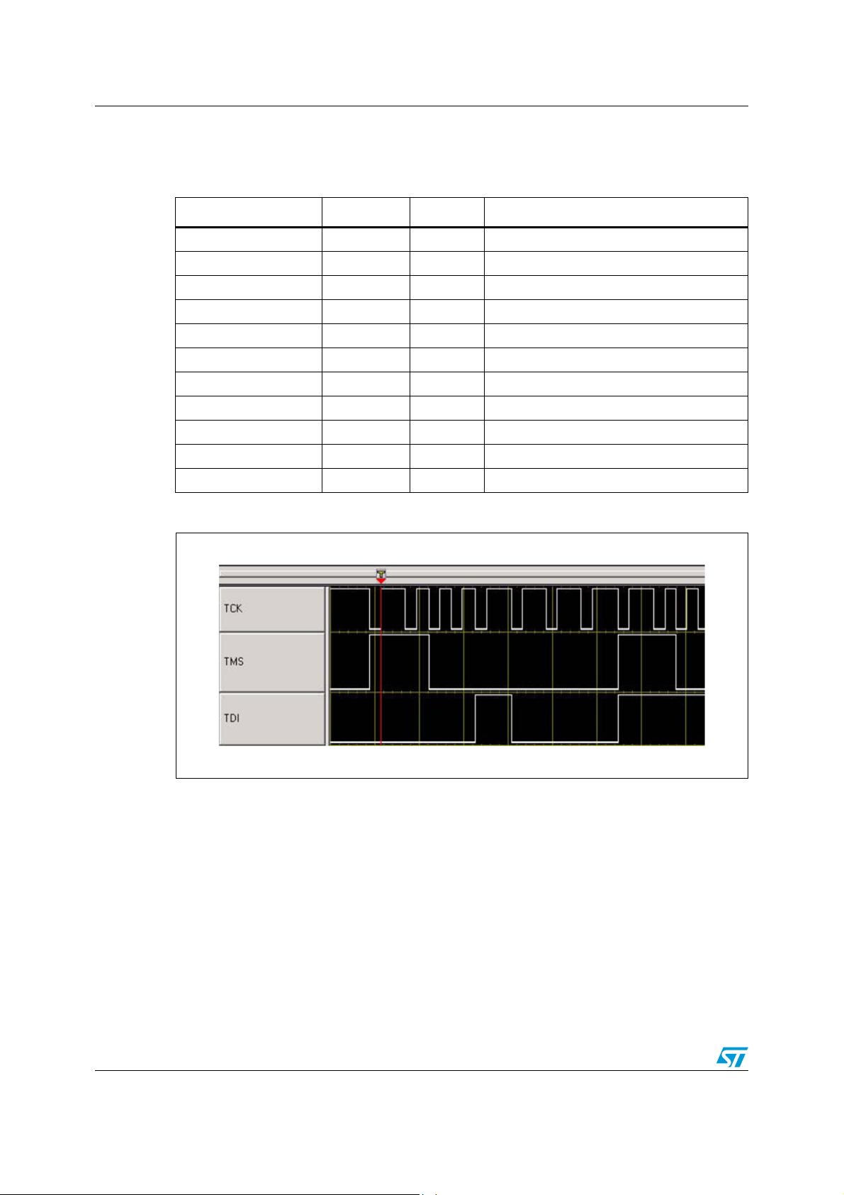
3.4 OnCE status register
The OnCE status register (OSR) is a special register in terms of how it is read. Status
information related to the state of the CPU is latched into the OnCE status register when the
OnCE TAP controller state machine enters the CAPTURE-IR state. The status information is
shifted out serially through the SHIFT-IR state on TDO. The OSR is a 10-bit register like the
OCMD. Therefore, the status information can be read while writing OCMD. The OSR is
shown in Figure 13.
Doc ID 022669 Rev 1 19/41
Page 20

On-Chip Emulation (OnCE) AN4035
Figure 13. OnCE status register
MCLK ERR CHKSTOP RESET HALT STOP DEBUG 0 1
0123456789
Figure 14 shows reading the OnCE status register on TDO while writing the OCMD on TDI
assuming the TAP controller state machine is initially in the RUN-TEST/IDLE state. The
state machine is returned to the RUN-TEST/IDLE state when the read is complete. The
OCMD is written with the value 0b10_0001_0001 choosing a read of No Register Selected.
The data read on TDO from the OnCE status register is 0b10_0000_1001 showing that the
OSR[MCLK] and OSR[DEBUG] status bits are set. All data is scanned in and out least
significant bit first.
Figure 14. Signal transitions of reading the OnCE status register
3.5 Entering debug mode during reset
There are several different methods of entering debug mode. This section covers entering
debug mode while the RESET pin is asserted. Entering debug mode while the RESET pin is
asserted is useful, because the debug session begins with the CPU in a known state. The
OnCE control register (OCR) controls entry into debug mode for this method. Figure 15
shows the register definition for the OCR.
Figure 15. OnCE control register
0DMDIS0DWDIDMDGDE0
0123456789101112131415 16 1718 19 20 21 22 23 24252627 28 29 30 31
The OCR[DR] bit is the CPU debug request control bit and requests the CPU to
unconditionally enter debug mode. The OCR[WKUP] bit is the wakeup request bit used to
guarantee that the CPU clock is running. Debug status and CPU clock activity can be
determined by reading the DEBUG and MCLK bits in the OnCE status register. After
20/41 Doc ID 022669 Rev 1
WK
UP
FDB DR
Page 21

AN4035 On-Chip Emulation (OnCE)
entering debug mode, the OCR[DR] bit should be cleared leaving the OCR[WKUP] bit set.
OCR[FDB] should also then be set to enable recognition of software breakpoints.
The steps required for entering debug mode during reset assuming the OnCE TAP controller
has been enabled are listed below:
1. Assert RESET.
2. Set the OCR[DR] and OCR[WKUP] bits.
3. De-assert RESET.
4. Verify debug mode via the DEBUG bit in the OnCE status register.
5. Clear the OCR[DR] bit while leaving OCR[WKUP] set and set OCR[FDB].
3.6 Enabling external debug mode and other initialization
Before enabling external debug mode, the CPU should be placed into debug mode via the
method outlined in the previous section.
The external tool should then write the DBCR0[EDM] bit to enable external debug mode.
Note that the first write to DBCR0 only affects the EDM bit. All other bits in that register
require DBCR0[EDM] to be set prior to writing them. After enabling external debug mode,
the DBSR status bits should be cleared by writing 0xFFFFFFFF to DBSR. The register
definition of DBSR is shown in Figure 16.
Figure 16. Debug Status Register (DBSR)
0123456789101112131415
IDE UDE MRR ICMP BRT IRPT TRAP IAC1 IAC2 IAC3 IAC4 DAC1RDAC1WDAC2RDAC
R
W
Reset0001000000000000
16 17 18 19 20 21 22 23 24 25 26 27 28 29 30 31
RRET0000
W
Reset0000000000000000
DEVT1DEV
DCNT1DCNT
T2
CIRPT CRET
2
0000
2W
CNT
1RG
3.7 CPU Status and Control Scan Chain Register (CPUSCR)
CPU information is accessible via the OnCE module through a single scan chain register
named the CPUSCR. The CPUSCR provides access to this CPU information and a
mechanism for an external tool to set the CPU to a desired state before exiting debug mode.
The CPUSCR also provides the ability to access register and memory contents. Figure 3-13
shows the CPUSCR. Once debug mode has been entered, it is required to scan in and
update the CPUSCR prior to exiting debug mode or single stepping. Access to the CPUSCR
is controlled by the OCMD.
Doc ID 022669 Rev 1 21/41
Page 22

On-Chip Emulation (OnCE) AN4035
Figure 17. CPU status and control scan chain register
7'2
7&.
:%%5
ORZ
7',
:%%5
KLJK
065
3.7.1 Instruction Register (IR)
After entering debug mode, the opcode of the next instruction to be executed is in the
instruction register (IR). The value in the IR should be saved for later restoration if
continuation of the normal instruction stream is desired.
The external tool has the capability to put instructions directly into the instruction register
(IR) via the CPUSCR. These instructions can then be executed by the debug control block.
By selecting appropriate instructions and single stepping them, the external tool can
examine or change memory locations or CPU registers.
3&
,5
&7/
22/41 Doc ID 022669 Rev 1
Page 23

AN4035 On-Chip Emulation (OnCE)
3.7.2 Control State Register (CTL)
The control state register (CTL) stores the value of certain internal CPU state variables
before debug mode is entered. Figure 18 shows the CTL register.
Figure 18. Control State Register (CTL)
*
PCOFST
012345678910111213141516171819202122232425262728293031
FFRA
PCINV
IRSTAT0
IRSTAT1
IRSTAT2
IRSTAT3
IRSTAT4
IRSTAT5
IRSTAT6
IRSTAT7
IRSTAT8
IRSTAT9
The “*” in the CTL register represents internal processor state bits that should be restored to
the value they held when debug mode was entered prior to exiting debug mode. If a single
step is executing an instruction that is in the normal instruction flow of the program that was
running when debug mode was entered, these bits should be restored. If a single step is
executing an instruction outside the normal instruction flow, these bits should be cleared to
zero.
The PCOFST field indicates whether the value in the PC portion of the CPUSCR must be
adjusted prior to exiting debug mode. Due to the pipelined nature of the CPU, the PC value
must be backed-up under certain circumstances. The PCOFST field specifies the value to
be subtracted from the PC value when debug mode was entered. This PC value should be
adjusted according to PCOFST prior to exit from debug mode if continuation of the normal
instruction stream is desired. In the event that PCOFST is non-zero, the IR should be loaded
with a nop instruction instead of the value in the IR when debug mode was entered.
Below are the possible values and meanings of the PCOFST field:
● 0000—No correction required.
● 0001—Subtract 0x04 from PC.
● 0010—Subtract 0x08 from PC.
● 0011—Subtract 0x0C from PC.
● 0100—Subtract 0x10 from PC.
● 0101—Subtract 0x14 from PC.
All other encodings are reserved.
After entering debug mode, the PCINV field overrides the PCOFST field and indicates that
values in the PC and IR are invalid. Exiting debug mode with these PC and IR values have
unpredictable results.
No error condition exists.
Error condition exists. PC and IR are corrupt.
The FFRA control bit causes the contents of WBBR to be used as the rA (rS for logical and
shift operations) operand value of the first instruction to be executed when exiting debug
mode or the instruction to be single stepped. This allows the external tool to update CPU
registers and memory. rA and rS are instruction syntax used to identify a source GPR.
No action.
Contents of WBBR used as rA (rS for logical and shift operations) operand value.
The IRStat0-9 bits provide status information to the external tool. The IRStat8 bit indicates
that the instruction in the IR is a VLE or non-VLE instruction. For MPC5500 devices without
Doc ID 022669 Rev 1 23/41
Page 24

On-Chip Emulation (OnCE) AN4035
VLE, bits IRstat8 and IRstat9 of the CTL do not exist. Below is a description of the IRStat8
bit.
All other CTL bits are discussed as needed.
IR contains a BookE instruction.
IR contains a PowerPC VLE instruction, aligned in the most significant portion of IR if
16-bit.
3.7.3 Program Counter Register (PC)
The PC stores the value of the program counter that was present when debug mode was
entered. The PC value is affected by operations performed during debug mode and must be
restored prior to exiting debug mode. It may be necessary to adjust the PC before exiting
debug mode according the PCOFST field in the CTL. If the external tool desires to redirect
program flow to an arbitrary location, the PC and IR should be initialized corresponding to
the first instruction to be executed. Alternatively, the IR may be set to a nop instruction and
the PC may be set to the location prior to the location at which it is desired to redirect flow.
When debug mode is exited, the nop executes and then instruction fetch and execution
begins at the location which it is desired to redirect flow.
3.7.4 Write-Back Bus Register (WBBR
WBBR is used as a means of passing operand information to/from the CPU from/to the
external tool. Whenever the external tool needs to read the contents of a CPU register or
memory location, it can force the CPU to single step an instruction that brings that
information to WBBR. To write the contents of a CPU register or memory location, the
external tool can force the CPU to single step an instruction that uses the information in
WBBR. For the purpose of this document, only WBBR
instructions that generate 64-bit results or use 64-bit operands. Such instructions are
outside the scope of this document.
3.7.5 Machine State Register (MSR)
The MSR is used to read/write the machine state register of the CPU. This register is
affected by operations performed while in debug mode. If consistency of the machine state
is desired, the MSR should be saved when entering debug mode and restored prior to
exiting debug mode.
3.8 Single step
Single stepping of instructions is achieved by first placing the CPU in debug mode if the
CPU is not already in debug mode. The next step is to write the appropriate information into
the CPU scan chain register (CPUSCR), followed by writing to OCMD to set the OCMD[GO]
bit and clear the OCMD[EX] bit with the OCMD[RS] field indicating either the CPUSCR or
No Register Selected. Once debug mode has been entered, it is required that a scan in and
update to the CPUSCR must be performed prior to single stepping. For single step, the CPU
returns to debug mode after executing a single instruction. The external tool should read the
OnCE status register (OSR) to verify that the CPU has returned to debug mode without the
OSR. During single step, exception conditions can occur, if not masked, and may prevent
the desired instruction from being executed. After stepping over the instruction, the core
fetches the next instruction. The new program counter and instruction are loaded into the
, WBBR
low
)
high
is used. WBBR
low
is used for SPE
high
24/41 Doc ID 022669 Rev 1
Page 25

AN4035 On-Chip Emulation (OnCE)
PC and IR portions of the CPUSCR. Care must be taken to insure that the next instruction
fetch after the single step is to a valid memory location.
For SPC56x devices with VLE, the CTL[IRstat8] bit indicates that the instruction in the IR is
a VLE or non-VLE instruction. The CTL[FFRA], CTL[IRStat8], and the CTL bits indicated by
“*” should be set as appropriate before single stepping. All other CTL bits should be set to
zero. Single stepping can be used during normal execution of the instruction flow or to force
execution of a particular instruction by loading the desired instruction into the IR portion of
the CPUSCR. By forcing execution of particular instructions, single stepping can be used for
memory and register access by the tool.
3.9 Exit from debug mode to normal execution
Exiting debug mode and returning to normal execution is achieved by first clearing the
OCR[DMDIS] and OCR[DR] bits if not already clear while leaving the OCR[MCLK] set. The
next step is to write the appropriate information into the CPU scan chain register
(CPUSCR), followed by a write to OCMD to set the OCMD[GO] bit and OCMD[EX] bit with
the OCMD[RS] field indicating either the CPUSCR or No Register Selected. Once debug
mode has been entered, it is required that a scan in and update to the CPUSCR be
performed prior to exiting debug mode. If continuation of the normal instruction stream is
desired, the external tool is responsible for inspection of the CTL register value when debug
mode was entered to determine if the PC is invalid or needs to be offset prior to exiting
debug mode. Also, the internal state bits indicated by “*” in the CTL should be restored to
their original value when debug mode was entered if continuation of the normal instruction
stream is desired. The IRStatus bits of the CTL should be set to zero with the exception of
CTL[IRStat8] on SPC56x devices with VLE. CTL[IRStat8] indicates if the current instruction
in the IR is a VLE or non-VLE instruction. To begin instruction execution from an arbitrary
location, the PC should be set to the desired location for execution to begin minus 0x4. The
IR should be set to a nop (ex: 0x60000000). Then exit debug mode as mentioned above.
The nop executes, then the core begins fetching instructions at the desired location for
execution.
3.10 GPR access
The OnCE module provides the ability to read and write the general purpose registers
(GPR) while in debug mode. Reading a general purpose register is achieved by single
stepping over an ori instruction. As an example, to read the lower 32 bits of GPR r1, an ori
r1,r1,0 instruction is executed, and the result of the instruction is latched into WBBR
external tool can then read the contents of WBBR
Writing a register is achieved by single stepping over an ori instruction with the CTL[FFRA]
bit set causing the WBBR
example, to write the lower 32 bit of GPR r1, an ori r1, X, 0 is executed with the data to be
written in WBBR
3.11 SPR access
The OnCE module provides the ability to read and write the special purpose registers (SPR)
while in debug mode. Reading a special purpose register is achieved by saving the value in
a GPR, single stepping over a mfspr instruction which brings the spr value into both the
by scanning out the CPUSCR.
low
to be used as the source register for the instruction. As an
low
. The X in the instruction is replaced by the WBBR
low
Doc ID 022669 Rev 1 25/41
register.
low
low
. The
Page 26

On-Chip Emulation (OnCE) AN4035
saved GPR and WBBR
, and then restoring the GPR. As an example, to read SPR 624,
low
first save r31. Then execute mfspr r31, 624. The value that was in SPR 624 is now in
WBBR
of the CPUSCR and can be read by the external tool. Finally r31 should be
low
restored.
To write an SPR, single step over a mtspr instruction with the value to write to the SPR in
WBBR
and the CTL[FFRA] bit set. For example, to write SPR 624 with the value
low
0x10050000, single step over mtspr 624, X with the value to write to SPR 624 in WBBR
and CTL[FFRA] set. The X in the instruction is replaced by WBBR
DBCR0-3, DBSR, DBCNT, IAC1-4, DAC1-2 cannot be written by single stepping over mtspr
like the other SPRs while in external debug mode. They can however be written by the
method detailed in Section 3.2: OnCE register access.
3.12 OnCE memory access
There are two ways to access memory mapped locations on the SPC56x devices: one is
through the OnCE module, and the other is through the Nexus R/W access block. The
OnCE module method requires that the CPU be in debug mode. The Nexus R/W access
block does not require that the CPU be in debug mode. The Nexus R/W access block is also
the faster method of accessing memory. This section covers access to memory mapped
locations using the OnCE method. The Nexus R/W access block is covered in a following
section.
Writing a memory location is achieved by first reading the contents of a GPR and saving that
value, writing that GPR with the value to be written to memory, and single stepping over a
stw, sth, or stb instruction with the address to write in WBBR
The GPR that was previously saved should be used as the rS field of the store instruction.
After single stepping over the store instruction, the saved GPR value should then be
restored. For example, to write the word 0xA5A5A5A5 to location 0x40000000, first save the
value in a r31. Then write the value 0xA5A5A5A5 to r31. The next step is to step over the
instruction stw r31, 0(X) with 0x40000000 in WBBR
the instruction is replaced by the WBBR
saved value.
Reading a memory location is achieved by first reading the contents of a GPR and saving
that value, then single stepping a lwz, lhz, or lbz with the address to be read in WBBR
and the CTL[FFRA] bit set. The GPR that was previously saved should be used as the rD
field of the load instruction. The value read from the memory location is then in both the
WBBR
After single stepping the load instruction and getting the read data from WBBR
GPR value should then be restored. For example, to read a word from address location
0x40000000, first save the value in r31. Then single step over the instruction lwz r31, 0(X)
with 0x40000000 in WBBR
replaced by the WBBR
memory can be read by the external tool from WBBR
to its saved value.
and the GPR whose value was previously saved.
low
and the CTL[FFRA] bit set. The X in the instruction is
low
register. After the single step is complete, the data read from
low
.
low
and the CTL[FFRA] bit set.
low
and the CTL[FFRA] bit set. The X in
register. GPR r31 should then be restored to its
low
low
, the saved
low
. GPR r31 should then be restored
low
low
low
3.13 Breakpoints
The OnCE debug module provides the capability for both software and hardware
breakpoints to be set at a particular address.
As a reference, instruction address hardware breakpoints is also discussed in this section.
26/41 Doc ID 022669 Rev 1
Page 27

AN4035 On-Chip Emulation (OnCE)
3.13.1 Software breakpoints
Recognition of software breakpoints by the OnCE module are enabled by setting the
OCR[FDB] bit along with the DBCR0[EDM] bit. Upon executing a bkpt pseudo-instruction,
the CPU enters debug mode after the instruction following the bkpt pseudo-instruction has
entered the instruction register. The bkpt pseudo-instruction is defined to be an all 0’s
instruction opcode.
3.13.2 Instruction address hardware breakpoints
The OnCE module provides the capability to set up to four instruction address hardware
breakpoints.
When an instruction address breakpoint is hit, the CPU enters debug mode prior to
executing the instruction at that address location. When debug mode is entered due to a
breakpoint, the CPUSCR holds the address at which the breakpoint was set in the PC, and
the IR contains the instruction at that address.
To use an instruction address hardware breakpoint, these steps are required:
1. Write the address at which a breakpoint is desired to one of the instruction address
compare registers IAC1, IAC2, IAC3, or IAC4.
2. Enable the instruction address compare debug event in the DBCR0 by setting the
appropriate enable bit; DBCR0[IAC1], DBCR0[IAC2], DBCR0[IAC3], or DBCR0[IAC4].
3. Exit from debug mode to normal execution to execute the desired code.
4. Poll the DBSR for the appropriate status bit to be set; DBSR[IAC1], DBSR[IAC2],
DBSR[IAC3], or DBSR[IAC4].
5. If the appropriate status bit in DBSR is set, verify entry into debug mode by reading the
OnCE status register.
6. Clear the appropriate status bit by writing a 1 to that bit location in the DBSR;
DBSR[IAC1], DBSR[IAC2], DBSR[IAC3], or DBSR[IAC4].
Doc ID 022669 Rev 1 27/41
Page 28
Nexus Read/Write access block AN4035
4 Nexus Read/Write access block
The Nexus module provided on the cores of the SPC56x family of devices offers the
capability for program trace, data trace, ownership trace, watchpoint messaging and trigger,
and read/write (R/W) access to memory mapped regions. This section covers R/W access
using the Nexus R/W access block. The other features of the Nexus module are out of the
scope of this document and is not covered.
Unlike the OnCE method of memory access, the Nexus R/W access block provides the
ability to read and write memory without having to stop code execution by entering debug
mode. The Nexus R/W access method provides faster memory access over the OnCE
method due to fewer JTAG scans, and it doesn’t require loading and single stepping over
any instructions. The Nexus R/W access block is independent of the CPU.
The R/W access block is controlled by three Nexus registers. These registers are the
Read/Write Access Control/Status register (RWCS), Read/Write Access Data register
(RWD), and Read/Write Access Address register (RWA). Access to the Nexus registers is
covered inSection 4.1. RWCS is shown in Figure 19 and Figure 5 gives the field
descriptions.
Figure 19. Read/Write Access Control/Status Register (RWCS)
31 30 29 28 27 26 25 24 23 22 21 20 19 18 17 16
R AC RW SZ MAP PR BST 0 0 0 0 0
W
Reset00000000000000000
Nexus
Reg
1514131211109876543210
R
W
Reset0000000000000000
Nexus
Reg
Table 5. RWCS field description
0x7
CNT ERR DV
0x7
Bits Name Description
Access control.
31 AC
0 End access
1 Start access
Read/write select.
30 RW
0 Read access
1 Write access
28/41 Doc ID 022669 Rev 1
Page 29

AN4035 Nexus Read/Write access block
Table 5. RWCS field description (continued)
Bits Name Description
Word size.
0008-bit (byte)
29–27
26–24
23–22
21 BST
SZ
[2:0]
MAP
[2:0]
PR
[1:0]
0016-bit (half-word)
01032-bit (word)
01164-bit (double-word - only in burst mode)
100–111 Reserved (default to word)
MAP select.
000Primary memory map
001-111 Reserved
Read/write access priority.
00Lowest access priority
01Reserved (default to lowest priority)
10Reserved (default to lowest priority)
11Highest access priority
BST Burst control.
0 Module accesses are single bus cycle at a time.
1 Module accesses are performed as burst operation.
20–16 — Reserved.
15–2
CNT
[13:0]
Access control count. Number of accesses of word size SZ.
1 ERR Read/write access error. See Table 4-2.
0 DV Read/write access data valid. See Table 4-2.
Ta bl e 6 details the status bit encodings.
Table 6. Read/Write access status bit encoding
Read action Write action ERR DV
Read access has not
completed
Read access error has
occurred
Read access
completed without error
Write access
completed without error
Write access error has
occurred
Write access has not
completed
00
10
01
Not allowed Not allowed 1 1
RWD is shown in Figure 20.
Doc ID 022669 Rev 1 29/41
Page 30

Nexus Read/Write access block AN4035
Figure 20. Read/Write access data register (RWD)
31 30 29 28 27 26 25 24 23 22 21 20 19 18 17 16
R
W
Reset0000000000000000
Nexus
Reg
15 14 13 12 11 10 9 8 7 6 5 4 3 2 1 0
R
W
Reset0000000000000000
Nexus
Reg
Read/Write Data
0xA
Read/Write Data
0xA
RWA is shown in Figure 21.
Figure 21. Read/Write access address register (RWA)
31 30 29 28 27 26 25 24 23 22 21 20 19 18 17 16
R
W
Reset0000000000000000
Nexus
Reg
15 14 13 12 11 10 9 8 7 6 5 4 3 2 1 0
R
W
Reset0000000000000000
Nexus
Reg
Read/Write Address
0x9
Read/Write Address
0x9
4.1 Nexus register access
Access to the Nexus registers is enabled by loading the Nexus3-Access instruction
(0b00_0111_1100) into the OCMD of the OnCE. Once the Nexus3-Access instruction has
been loaded, reading/writing a Nexus register requires two passes through the DR path the
OnCE TAP controller state machine that are detailed below.
1. The first pass through the DR selects the Nexus register to be accessed and whether
the access is a read or a write. This is achieved by loading an 8-bit value LSB first into
the JTAG Data Register (DR). The format of this register is described in Table 7 .
30/41 Doc ID 022669 Rev 1
Page 31

AN4035 Nexus Read/Write access block
Table 7. JTAG Data Register (DR)
(7-bits) (1-bit)
Nexus Register Index R/W
RESET Value: 0x00
Table 8. Nexus register index
Nexus register index Value shown at bottom of register description
Read/Write (R/W)
0 Read
1 Write
2. The second pass through the DR then shifts the data in or out depending on the type of
access LSB first.
a) During a read access, the data is latched from the Nexus register when the TAP
controller state machine passes through the CAPTURE-DR state. The data from
the Nexus register can be read by the external tool by shifting the data out in the
SHIFT-DR state. The last bit is shifted out with TMS set to 1, causing transition to
the EXIT1-DR state.
b) During a write access, the data is shifted in while in the SHIFT-DR state. The last
bit is shifted in with TMS set to 1, causing transition to the EXIT1-DR state. The
data is latched into the Nexus register when the TAP controller state machine
passes through the UPDATE-DR state.
Doc ID 022669 Rev 1 31/41
Page 32

Nexus Read/Write access block AN4035
4.2 Single memory write access
The steps to perform a single memory write access via the Nexus R/W access block are:
1. Initialize RWA with the address to be written using Nexus register index 0x9.
2. Initialize RWCS using Nexus register index 0x7.
a) Access Control (AC) = 0b1 (to indicate start access)
b) Map Select (MAP) = 0b000 (primary memory map)
c) Access Priority (PR) = 0b00 (lowest priority)
d) Read/Write (RW) = 0b1 (write access)
e) Word Size (SZ) = 0b000 (8-bit) or 0b001 (16-bit) or 0b010 (32-bit)
f) Access Count (CNT) = 0b00_0000_0000_0000 or 0b00_0000_0000_0001 (single
access)
g) Burst Control (BST) = 0b0 (burst disabled)
3. Initialize RWD using Nexus register index 0xA with the data to be written to the address
in RWA. The endianess of the data needs to be right-justified little endian.
- 8-bit value of 0xDE to be written to memory: RWD = 0x000000DE
- 16-bit value of 0xDEAD to be written to memory: RWD = 0x0000ADDE
- 32-bit value of 0xDEADBEEF to be written to memory: RWD = 0xEFBEADDE
4. The Nexus block then arbitrates for the system bus and transfer the data value from
RWD to the memory mapped address in RWA. When the access has completed
without error, then RWCS[ERR] = 0 and RWCS[DV] = 0. This indicates that the device
is ready for the next access. Nexus also asserts the RDY pin when the transaction has
completed without error. The external tool can use this as an alternative to polling the
RWCS status bits.
4.3 Burst block memory write access
The steps to perform a burst block memory write access via the Nexus R/W access block
are:
1. Initialize RWA with the first address to be written using Nexus register index 0x9. The
address needs to be aligned on an 8-byte boundary. RWA[2:0] are ignored on a burst
write.
2. Initialize RWCS using Nexus register index 0x7.
a) Access Control (AC) = 0b1 (to indicate start access)
b) Map Select (MAP) = 0b000 (primary memory map)
c) Access Priority (PR) = 0b00 (lowest priority)
d) Read/Write (RW) = 0b1 (write access)
e) Word Size (SZ) = 0b011 (64-bit)
f) Access Count (CNT) = 0b00_0000_0000_0100 (four double-words)\
g) Burst Control (BST) = 0b1 (burst enabled)
3. Write all 32 bytes of data to be burst to RWD using Nexus register index 0xA, 32-bits at
a time, starting with the first 32-bit word to be written to the address in RWA. This data
32/41 Doc ID 022669 Rev 1
Page 33

AN4035 Nexus Read/Write access block
is buffered internally by the burst data buffer. The endianess of the 32-bit data written to
RWD needs to be little endian.
-Value of 0xDEADBEEF to be written to memory: RWD = 0xEFBEADDE
4. The Nexus block then arbitrates for the system bus and transfer the burst data from the
burst data buffer to the memory starting at the address in RWA. When the access has
completed without error, then RWCS[ERR] = 0 and RWCS[DV] = 0. This indicates that
the device is ready for the next access. Nexus also asserts the RDY pin when the
transaction has completed without error. The external tool can use this as an
alternative to polling the RWCS status bits.
4.4 Single memory read access
The steps to perform a single memory read access via the Nexus R/W access block are:
1. Initialize RWA with the address to be read using the register index 0x9.
a) Initialize RWCS using Nexus register index 0x7.
b) Access Control (AC) = 0b1 (to indicate start access)
c) Map Select (MAP) = 0b000 (primary memory map)
d) Access Priority (PR) = 0b00 (lowest priority)
e) Read/Write (RW) = 0 (read access)
f) Word Size (SZ) = 0b000 (8-bit) or 0b001 (16-bit) or 0b010 (32-bit)
g) Access Count (CNT) = 0b00_0000_0000_0000 or 0b00_0000_0000_0001 (single
access)
h) Burst Control (BST) = 0b0 (burst disabled)
2. The Nexus block then arbitrates for the system bus and the read data is transferred to
RWD from the memory mapped address in RWA. When the access has completed
without error, then RWCS[ERR] = 0 and RWCS[DV] = 1. This indicates that the device
is ready for the next access. Nexus also asserts the RDY pin when the transaction has
completed without error. The external tool can use this as an alternative to polling the
RWCS status bits.
3. The data can then be read from the RWD register using Nexus register index 0xA. The
data in RWD are right-justified little endian.
- 8-bit value of 0xDE read from memory: RWD = 0x000000DE
- 16-bit value of 0xDEAD read from memory: RWD = 0x0000ADDE
- 32-bit value of 0xDEADBEEF read from memory: RWD = 0xEFBEADDE
Doc ID 022669 Rev 1 33/41
Page 34

Nexus Read/Write access block AN4035
4.5 Burst block memory read access
The steps to perform a burst block memory read access via the Nexus R/W access block
are:
1. Initialize RWA with the first address to be read using Nexus register index 0x9. The
address needs to be aligned on an 8-byte boundary. RWA[2:0] are ignored on a burst
read.
2. Initialize RWCS using Nexus register index 0x7.
- Access Control (AC) = 0b1 (to indicate start access)
- Map Select (MAP) = 0b000 (primary memory map)
- Access Priority (PR) = 0b00 (lowest priority)
- Read/Write (RW) = 0b0 (read access)
- Word Size (SZ) = 0b011 (64-bit)
- Access Count (CNT) = 0b00_0000_0000_0100 (four double-words)-
- Burst Control (BST) = 0b1 (burst enabled)
3. The Nexus block then arbitrates for the system bus and transfer the burst data from
memory to the burst data buffer starting at the address in RWA. When the access has
completed without error then RWCS[ERR] = 0 and RWCS[DV] = 1. See Ta bl e 8 for
details. This indicates that the device is ready for the next access. Nexus also asserts
the RDY pin when the transaction has completed without error. The external tool can
use this as an alternative to polling the RWCS status bits.
4. Read all 32 bytes of data from RWD using Nexus register index 0xA, 32-bits at a time,
starting with the first 32-bit word read from the address in RWA. The endianess of the
32-bit data read from RWD is little endian.
- Value of 0xDEADBEEF read from memory: RWD = 0xEFBEADDE
34/41 Doc ID 022669 Rev 1
Page 35

AN4035 System initialization
5 System initialization
For Flash programming, there is some system initialization that needs to be performed by
the external tool.
The initialization to perform is the SRAM initialization.
5.1 Internal SRAM initialization
The SPC56x family of devices all contain internal SRAM that must be initialized after poweron-reset by 64-bit writes to the entire memory. This is necessary to initialize the errorcorrecting code (ECC) logic.
The easiest way to do this with an external tool is to single step over a number of stmw
(store multiple words) instructions with r0 as the rS field, the address to begin the writes in
WBBR
at the address in WBBR
the internal SRAM is 0x40000000. Stepping over stmw r0, 0(X) with the 0x40000000 in
WBBR
using 64-bit writes. Then 0x80 should be added to the address, written to WBBR
stmw executed again. This should be done [size of internal SRAM] / [0x80] times to initialize
the entire internal SRAM.
, and CTL[FFRA] set. This causes all 32 GPRs to be written to memory beginning
low
causes all 32 GPRs to be written to memory starting at address 0x40000000
low
using 64-bit writes. For example, the starting physical address of
low
and
low
5.2 Setting up the memory management unit
The memory management unit (MMU) on the SPC56x devices, that include this hardware
implementation (for example SPC560B devices don’t have this hardware implementation),
provides memory translation from effective to real addresses. For the purpose of Flash
programming, it is easiest to setup the MMU such that the effective addresses are the same
as the real addresses. For the CPU to access a memory mapped region, an MMU entry for
that memory space must be configured. The external tool has the capability to setup MMU
entries by writing the appropriate SPRs and single stepping over the tlbwe instruction.
For Flash programming, the external tool should set up at least four MMU entries. The steps
required to setup an MMU entry are:
1. Setup MAS0 (SPR 624).
2. Setup MAS1 (SPR 625).
3. Setup MAS2 (SPR 626).
4. Setup MAS3 (SPR 627).
5. Execute tlbwe (0x7C0007A4).
Doc ID 022669 Rev 1 35/41
Page 36

Creating the Flash programming tool AN4035
6 Creating the Flash programming tool
This section covers the Flash drivers provided by STMicroelectronic®, the tool requirements,
and also suggests a functional division of the tool.
6.1 Flash programming drivers
STMicroelectronics provides a set of Flash drivers called Standard Software Driver for
C90FL Flash (SSD). These drivers are easy to use and well documented. The drivers come
in a c-array format, s-record format, and library format. For external tools, the s-record
format is the easiest to use. Instructions on how to use the s-record format set of drivers is
discussed in the next section. There are also examples of using the three driver formats
provided with the installation of the SSD.
6.2 Tool requirements
The Flash programming tool must perform several required tasks to program the Flash on
the SPC56x devices.
6.2.1 Debug and driver initialization
The first requirement is to enter debug mode followed by the appropriate initialization. These
steps must be performed every time a reset occurs or a new SPC56x device is connected to
the Flash programming tool. The steps to do this are listed below.
1. Ensure that the JTAGC currently has control of the TAP by going through the PAUSEDR state. See Section 2.4.2: Test mode for details.
2. Enable the OnCE TAP controller by the method outlined in Section 3.1: Enabling the
OnCE TAP controller.
3. Enter debug mode during reset and enable recognition of software breakpoints as
mentioned in Section 3.5: Entering debug mode during reset.
4. Enable external debug mode and clear the debug status bits as mention in Section 3.6:
Enabling external debug mode and other initialization.
5. Setup the MMU as described in Section 5.2: Setting up the memory management unit.
If it is necessary depending on the device used.
6. Initialize the internal SRAM as mentioned in Section 5.1: Internal SRAM initialization.
The next step is to load the s-record format Flash driver set. The required drivers to load are
FlashInit, SetLock, FlashProgram, and FlashErase. The other drivers are not required but
could be loaded if features other than erasing and programming are desired. The s-record
drivers all specify the start address to be 0x0 however the drivers are position independent.
The tool should load each driver into internal SRAM at a desired location. The tool is
responsible for knowing where these drivers are located in memory. Space should also be
reserved in the internal SRAM for variables needed for the driver set. For example, the
SSD_CONFIG structure is used for all drivers.
Space must be allocated for this structure. Space should also be allocated in internal SRAM
for the stack and a buffer for the data to be programmed to Flash. The drivers and variables
can be written by the method described Section 3.12: OnCE memory access or the
methods described in Section 4: Nexus Read/Write access block.
36/41 Doc ID 022669 Rev 1
Page 37

AN4035 Creating the Flash programming tool
6.2.2 FlashInit
After the drivers are loaded into internal SRAM, operations on the Flash can begin. The
FlashInit driver should be called first to initialize the Flash.
This function reads the Flash configuration information from the Flash control registers and
initialize parameters in SSD configuration structure. ‘FlashInit()’ must be called prior to any
other flash operations.
The steps required are outlined below.
1. Setup the SSD_CONFIG structure as required. This is documented in the SSD user’s
manual. The user should correctly initialize the fields c90flRegBase, mainArrayBase,
shadowRowBase, shadowRowSize, pageSize, and BDMEnable. The other fields are
initialized when FlashInit is executed. BDMEnable should be set to 1 to cause debug
mode to be entered via a software breakpoint when each driver completes execution.
This is the easiest way for the external tool to determine when driver execution is
complete.
2. Setup r1 as the stack pointer by writing r1 using the method described in Section 3.10:
GPR access.
3. Setup r3 to point to the SSD_CONFIG structure in internal SRAM.
4. Set the PC to the beginning of FlashInit minus 0x4 and load the IR with a nop
(0x60000000). See Section 3.7: CPU Status and Control Scan Chain Register
(CPUSCR) for details.
5. Exit debug mode and begin execution of the driver as described in Section 3.9: Exit
from debug mode to normal execution.
6. Poll the OnCE Status Register to determine when debug mode has been re-entered.
Reading the OnCE Status Register is described in Section 3.4: OnCE status register.
7. When debug mode has been entered, read the return value in r3.
6.2.3 SetLock
After the Flash has been initialized using the FlashInit function, the SetLock function should
be called as many times as required to unlock or lock the appropriate Flash blocks. This
function sets the block lock state for Shadow/Low/Middle/High address space on the C90FL
module to protect them from program/erase. The API provides password to enable block
lock register writes when needed and write the block lock value to block lock register for the
requested address space.
For the low and mid blocks as well as the shadow block, the lock bits in both the primary and
secondary lock registers must be set appropriately. It is recommended to lock the shadow
block unless programming of the shadow block is absolutely necessary. Erasing the shadow
block without re-programming the censorship information prior to a reset causes the device
to be censored with an invalid password and the Flash of the device is not able to be
uncensored.
The steps to call the SetLock driver are listed below.
Doc ID 022669 Rev 1 37/41
Page 38

Creating the Flash programming tool AN4035
1. Setup r1 as the stack pointer.
2. Setup r3 to point to the SSD_CONFIG structure in internal SRAM.
3. Setup r4 with the lock indicator.
4. Setup r5 with the lock state.
5. Setup r6 with the correct password.
6. Set the PC to the beginning of SetLock minus 0x4 and load the IR with a nop
(0x60000000).
7. Exit debug mode and begin execution of the driver.
8. Poll the OnCE Status Register to determine when debug mode has been re-entered.
9. When debug mode has been entered, read the return value in r3.
6.2.4 FlashErase
When the appropriate blocks have been locked or unlocked, then an erase of the unlocked
blocks can be performed.
This function erases the enabled blocks in the main array or the shadow row. Input
arguments together with relevant Flash module status is checked, and relevant error code
returns if there is any error.
The steps to call the FlashErase driver are listed below.
1. Setup r1 as the stack pointer.
2. Setup r3 to point to the SSD_CONFIG structure in internal SRAM.
3. Setup r4 to indicate either the main array or shadow block to be erased. Erasing the
shadow block without re-programming the censorship control information prior to a
reset results in the device being censored.
4. Setup r5 to select the low address array blocks to be erased.
5. Setup r6 to select the mid address array blocks to be erased.
6. Setup r7 to select the high address array blocks to be erased.
7. Setup r8 with the pointer to the call back function.
8. Set the PC to the beginning of FlashErase minus 0x4 and load the IR with a nop
(0x60000000).
9. Exit debug mode and begin execution of the driver.
10. Poll the OnCE Status Register to determine when debug mode has been re-entered.
11. When debug mode has been entered, read the return value in r3.
6.2.5 FlashProgram
When Flash blocks have been erased, they then can be programmed. To program the Flash,
the internal SRAM should first be written with the data to be programmed in Flash.
Depending on the size of the data buffer in internal SRAM and the size of the data to be
programmed to Flash, the FlashProgram driver may need to be called multiple times.
This function programs the specified flash areas with the provided source data. Input
arguments together with relevant flash module status is checked, and relevant error code is
returned if there is any error.
The steps to call the FlashProgram driver are listed below.
38/41 Doc ID 022669 Rev 1
Page 39

AN4035 Creating the Flash programming tool
1. Setup r1 as the stack pointer.
2. Setup r3 to point to the SSD_CONFIG structure in internal SRAM.
3. Setup r4 to point to the destination address to be programmed in Flash. This address
must be aligned on a double word boundary.
4. Setup r5 to the size of the data in bytes to be programmed to Flash. This size should be
a multiple of 8 and the combination of the destination address and size should be
entirely contained in the main array or shadow block.
5. Setup r6 to point to the source buffer of data in internal SRAM to be programmed to
Flash. This address should be aligned on a word boundary.
6. Setup r7 with the pointer to the call back function.
7. Set the PC to the beginning of FlashProgram minus 0x4 and load the IR with a nop
(0x60000000).
8. Exit debug mode and begin execution of the driver.
9. Poll the OnCE Status Register to determine when debug mode has been re-entered.
10. When debug mode has been entered, read the return value in r3.
6.2.6 Using other drivers
There are other useful drivers provided with the driver set. For example, BlankCheck can be
used to verify that a particular region is erased, and ProgramVerify can be used to verify that
the data was programmed correctly. The method to use these other drivers is similar to the
above mentioned drivers except that the GPRs needs to be setup appropriately for that
particular driver.
Doc ID 022669 Rev 1 39/41
Page 40

Creating the Flash programming tool AN4035
6.3 Functional division of the external tool
Before creating the external tool for Flash programming, thought should be given to how the
software should be divided to meet the tool’s functional requirements. The following list
gives an example of a simple functional division of the software:
● OnCE TAP controller enable, Section 3.1: Enabling the OnCE TAP controller.
● OnCE register read, Section 3.2: OnCE register access.
● OnCE register write, Section 3.2: OnCE register access.
● OnCE status register read, Section 3.4: OnCE status register.
● Debug mode during reset, Section 3.5: Entering debug mode during reset.
● Single step, Section 3.8: Single step.
● Exit from debug mode, Section 3.9: Exit from debug mode to normal execution.
● Write GPR, Section 3.10: GPR access.
● Read GPR, Section 3.10: GPR access.
● Write SPR, Section 3.11: SPR access.
● Read SPR, Section 3.11: SPR access.
● OnCE memory read, Section 3.12: OnCE memory access.
● OnCE memory write, Section 3.12: OnCE memory access.
● Nexus3 single write, Section 4.2: Single memory write access.
● Nexus3 burst write, Section 4.3: Burst block memory write access.
● Nexus3 single read, Section 4.4: Single memory read access.
● Nexus3 burst read, Section 4.5: Burst block memory read access.
● MMU initialization, Section 5.2: Setting up the memory management unit.
● Internal SRAM initialization,Section 5.1: Internal SRAM initialization.
● S-record parser and loader.
● Debug and driver initialization, Section 6.2.1: Debug and driver initialization.
● Flash initialization, Section 6.2.2: FlashInit.
● Flash block lock initialization, Section 6.2.3: SetLock.
● Flash erase, Section 6.2.4: FlashErase.
● Flash program, Section 6.2.5: FlashProgram.
40/41 Doc ID 022669 Rev 1
Page 41

AN4035
Please Read Carefully:
Information in this document is provided solely in connection with ST products. STMicroelectronics NV and its subsidiaries (“ST”) reserve the
right to make changes, corrections, modifications or improvements, to this document, and the products and services described herein at any
time, without notice.
All ST products are sold pursuant to ST’s terms and conditions of sale.
Purchasers are solely responsible for the choice, selection and use of the ST products and services described herein, and ST assumes no
liability whatsoever relating to the choice, selection or use of the ST products and services described herein.
No license, express or implied, by estoppel or otherwise, to any intellectual property rights is granted under this document. If any part of this
document refers to any third party products or services it shall not be deemed a license grant by ST for the use of such third party products
or services, or any intellectual property contained therein or considered as a warranty covering the use in any manner whatsoever of such
third party products or services or any intellectual property contained therein.
UNLESS OTHERWISE SET FORTH IN ST’S TERMS AND CONDITIONS OF SALE ST DISCLAIMS ANY EXPRESS OR IMPLIED
WARRANTY WITH RESPECT TO THE USE AND/OR SALE OF ST PRODUCTS INCLUDING WITHOUT LIMITATION IMPLIED
WARRANTIES OF MERCHANTABILITY, FITNESS FOR A PARTICULAR PURPOSE (AND THEIR EQUIVALENTS UNDER THE LAWS
OF ANY JURISDICTION), OR INFRINGEMENT OF ANY PATENT, COPYRIGHT OR OTHER INTELLECTUAL PROPERTY RIGHT.
UNLESS EXPRESSLY APPROVED IN WRITING BY TWO AUTHORIZED ST REPRESENTATIVES, ST PRODUCTS ARE NOT
RECOMMENDED, AUTHORIZED OR WARRANTED FOR USE IN MILITARY, AIR CRAFT, SPACE, LIFE SAVING, OR LIFE SUSTAINING
APPLICATIONS, NOR IN PRODUCTS OR SYSTEMS WHERE FAILURE OR MALFUNCTION MAY RESULT IN PERSONAL INJURY,
DEATH, OR SEVERE PROPERTY OR ENVIRONMENTAL DAMAGE. ST PRODUCTS WHICH ARE NOT SPECIFIED AS "AUTOMOTIVE
GRADE" MAY ONLY BE USED IN AUTOMOTIVE APPLICATIONS AT USER’S OWN RISK.
Resale of ST products with provisions different from the statements and/or technical features set forth in this document shall immediately void
any warranty granted by ST for the ST product or service described herein and shall not create or extend in any manner whatsoever, any
liability of ST.
ST and the ST logo are trademarks or registered trademarks of ST in various countries.
Information in this document supersedes and replaces all information previously supplied.
The ST logo is a registered trademark of STMicroelectronics. All other names are the property of their respective owners.
© 2012 STMicroelectronics - All rights reserved
STMicroelectronics group of companies
Australia - Belgium - Brazil - Canada - China - Czech Republic - Finland - France - Germany - Hong Kong - India - Israel - Italy - Japan -
Malaysia - Malta - Morocco - Philippines - Singapore - Spain - Sweden - Switzerland - United Kingdom - United States of America
www.st.com
Doc ID 022669 Rev 1 41/41
 Loading...