

Page 1

AN4030
Application note
Gate to cathode capacitor, impact on Triac immunity and reliability
Introduction
Triacs and SCRs are power semiconductors which are usually directly connected to the grid
line. As is well known, the AC grid voltage can be highly perturbed by important voltage
variation during very short times, for example, mechanical relay contact bounce, universal
motor disturbances. Several electromagnetic standards describe how appliances have to be
tested to check their immunity to such events. For example, the IEC 61000-4-4 standard
gives the test procedures and immunity requirements respectively for fast transient voltages.
To increase power-semiconductor device immunity, most designers add a capacitor across
the power device control terminal (the gate for SCRs or Triacs) and its reference terminal (K
or A1 respectively for SCRs and Triacs). This capacitor helps stabilize the control terminal
potential and so is believed to help increase resistance to fast voltage rises (dV/dt). As this
capacitor is also placed between the power device and the control circuit, which could be a
logic gate or a microcontroller unit (MCU), it acts as a filter on the path from the line to the
sensitive control circuit, and helps filter the noise coming from line disturbances.
This paper demonstrates why a gate to cathode capacitor is not efficient to improve Triac
immunity to fast voltage transients, especially for non-sensitive devices. This Application
note demonstrates that such capacitors can increase the risk of failure for repetitive or
accidentally high dI/dt.
The results presented in this Application note have been produced over a considerable
period of time. Some products, which are used as examples to present these results, may
no longer be available. However, the results presented apply to classes and types of
product, and thus are equally applicable to similar products available in the market.
March 2012 Doc ID 022635 Rev 1 1/15
www.st.com
Page 2

Contents AN4030
Contents
1 Gate to cathode capacitor, impact on dV/dt immunity . . . . . . . . . . . . . 3
1.1 dV/dt test method . . . . . . . . . . . . . . . . . . . . . . . . . . . . . . . . . . . . . . . . . . . . 3
1.2 dV/dt improvement for SCR . . . . . . . . . . . . . . . . . . . . . . . . . . . . . . . . . . . . 4
1.3 Behavior of Triacs regarding dV/dt . . . . . . . . . . . . . . . . . . . . . . . . . . . . . . 6
1.4 Behavior of Triacs to EFT (electrical fast transient) . . . . . . . . . . . . . . . . . . 8
2 Gate to cathode capacitor, impact on dI/dt capability . . . . . . . . . . . . . 11
3 Conclusion . . . . . . . . . . . . . . . . . . . . . . . . . . . . . . . . . . . . . . . . . . . . . . . . 13
4 Revision history . . . . . . . . . . . . . . . . . . . . . . . . . . . . . . . . . . . . . . . . . . . 14
2/15 Doc ID 022635 Rev 1
Page 3
AN4030 Gate to cathode capacitor, impact on dV/dt immunity
1 Gate to cathode capacitor, impact on dV/dt immunity
1.1 dV/dt test method
To characterize device immunity, semiconductor companies give the maximum dV/dt rate
which can be applied across a device without a risk of triggering it.
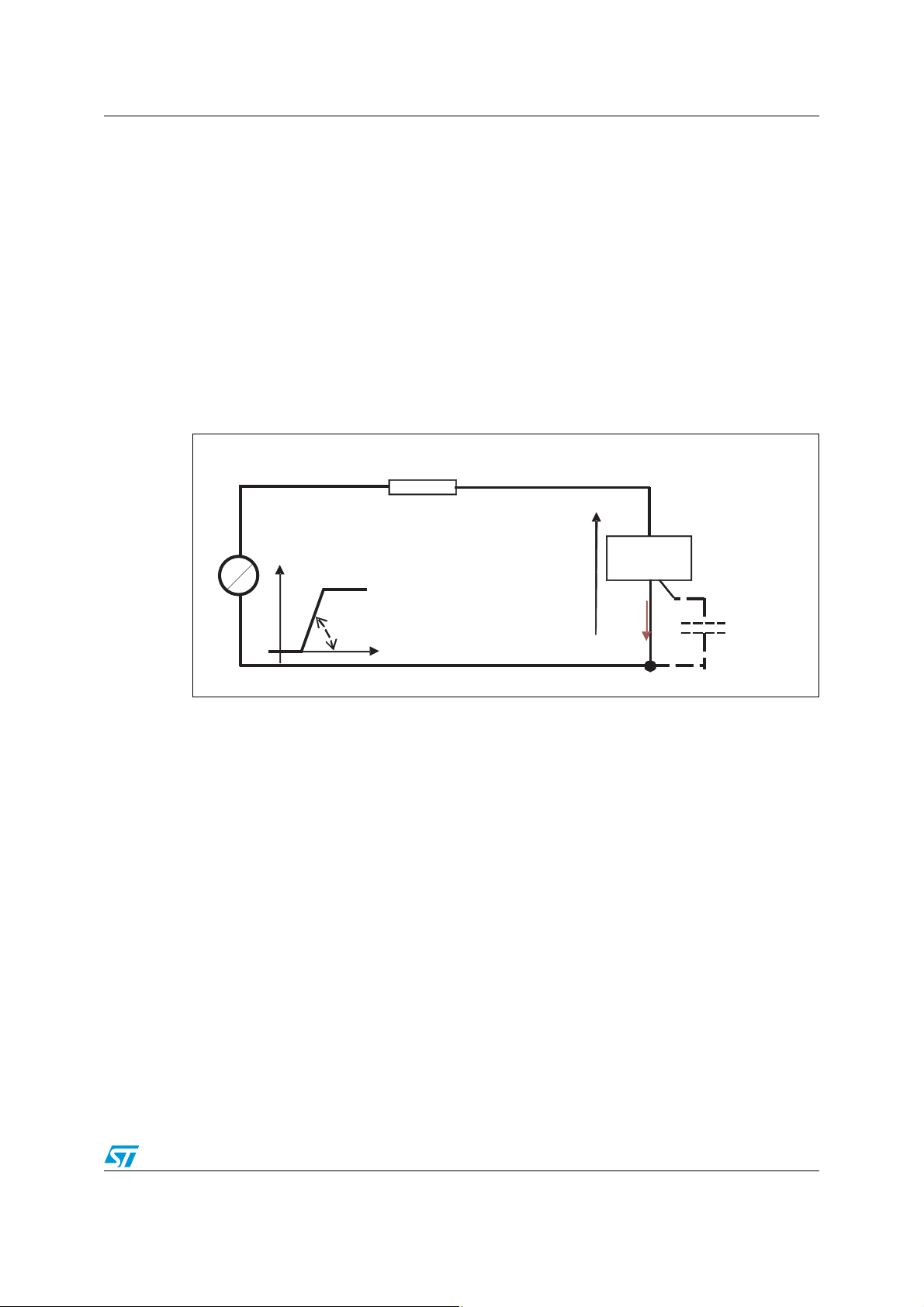
The test schematic features a dV/dt generator which applies a voltage-versus-time linear
slope (see Figure 1). The test equipment detects if the voltage across the DUT (device
under test) decreases below a given threshold. For a given dV/dt level, if the device voltage
drops below this threshold, this means that the device has switched on. The DUT capability
is then lower than this dV/dt rate. The dV/dt parameter specified in the device datasheet is
then the minimum rate that all devices were able to withstand during the tests.
Figure 1. dV/dt test simplified schematic
20 Ω
dV/dt generator
(LEMSYS 50)
V
+
V
(Fixed value: usually 67% x V
dV/dt
peak
t
<V
DRM
V
DRM
T
Device
under test
I
T
Triac
or
SCR
Gate to
cathode
capacitor
The dV/dt parameter is usually measured under the following conditions:
● Peak applied voltage = 67% of V
●
Maximum junction temperature (125 °C most of the time)
● Gate open
DRM
These test conditions are the worst case, as the dV/dt immunity decreases if both the
junction temperature and the impedance between G and K increase.
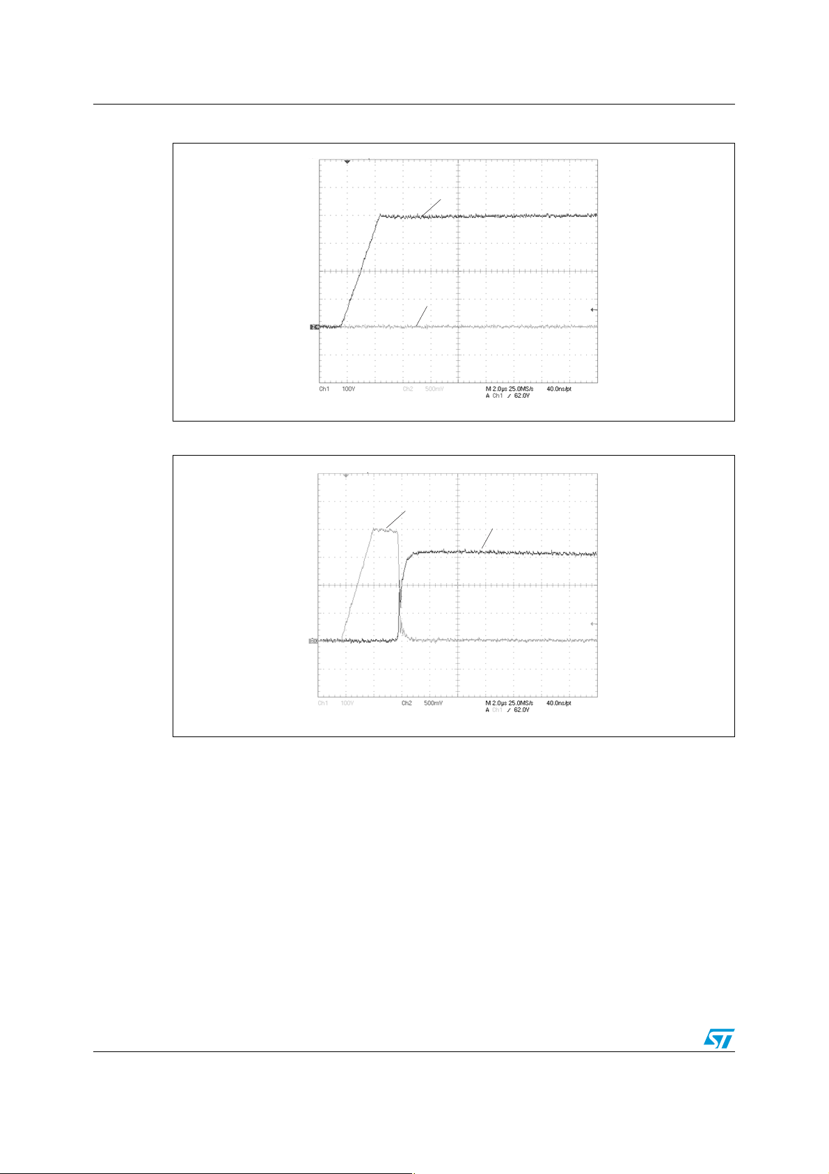
The following figures give an example of a 600 V SCR dV/dt measurement. A 402 V peak
voltage is applied, as it represents 67% of the specified V
. In Figure 2, the device
DRM
remains off. There is no current increase. In Figure 3, the same device switches on
approximately 2 µs after the voltage reaches its peak and stable level. According to these
two results, it could be said that the tested SCR is able to withstand a 150 V/µs rate.
Doc ID 022635 Rev 1 3/15
Page 4
Gate to cathode capacitor, impact on dV/dt immunity AN4030
Figure 2. c test with a 150 V/µs slope
V
T
402 V
I
T
Figure 3. 600 V SCR test with a 160 V/µs slope
V
402 V
1.2 dV/dt improvement for SCR
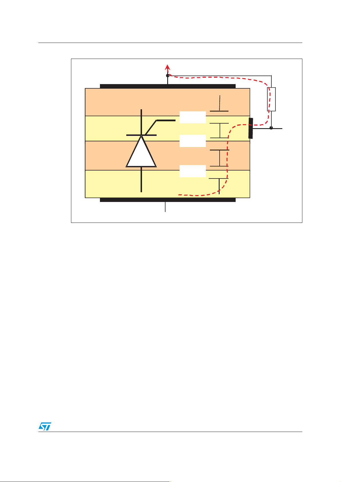
To understand why a semiconductor can be triggered by a dV/dt slope applied across its
terminals, it should be kept in mind that semiconductor devices are composed of several
silicon layers. An SCR features four layers, alternatively doped by holes (P area) or by
electrons (N area). Each PN junction presents a spurious capacitance (see Figure 4). When
a voltage slope is applied, a spurious capacitive current (I
capacitances. This current can then flow to the cathode through the P1-N1 junction and
cause device switch-on. To solve this issue, an impedance, for example a resistor (refer to
gate to cathode resistor in Figure 4), could be added between the gate and cathode
terminals. The spurious capacitive current is then shunted and avoids the device being
triggered.
T
I
T
) is induced by these
CAP
4/15 Doc ID 022635 Rev 1
Page 5
AN4030 Gate to cathode capacitor, impact on dV/dt immunity
Figure 4. SCR simplified silicon structure and spurious capacitive current
I
CAP
Cathode (K)
N1
P1
N2
P2
C
N1/P1
C
P1/N2
C
N2/P2
Anode (A)
R
GK
Gate (G)
A better solution could be found if a capacitor is used instead of a resistor. A high-voltage
gate to cathode capacitor is not necessary because only a low voltage (V
is around 1 V
GK
typically) is applied across this capacitor.
Figure 5 shows the typical relative dV/dt increase versus gate-cathode capacitance for an
8 A sensitive SCR series (I
max = 0.2 mA). The SCR dV/dt could be improved more than
GT
ten times with a 100 nF gate to cathode capacitor.
It should be noted that a gate to cathode resistor is still used in parallel with the gate to
cathode capacitor to discharge it after gate current removal.
For non–sensitive SCRs (I
above around 5 mA), a gate to cathode capacitor does not
GT
improve dV/dt immunity a lot. Indeed, these devices already feature a very low internal gate
to cathode resistor. So adding any external component is not very efficient to shunt the
spurious capacitive current.
Doc ID 022635 Rev 1 5/15
Page 6

Gate to cathode capacitor, impact on dV/dt immunity AN4030
Figure 5. SCR dV/dt increase versus added gate to cathode capacitor
dV/dt [CGK] / dV/dt [RGK= 220 ]Ω
15.0
12.5
10.0
7.5
5.0
VD= 0.67 x V
RGK=220 Ω
Tj=125
°C
DRM
2.5
0.0
0 20 100 160 200
40 60 80 120 140 180
CGK(nF)
1.3 Behavior of Triacs regarding dV/dt
A Triac silicon structure differs from an SCR structure. First, Triacs can conduct current in
both directions. A Triac is equivalent to 2 SCRs back-to-back with a common gate. The real
gate area of the reverse SCR is on the opposite side of the gate terminal connection (see
Figure 6).
Figure 6. Triac simplified silicon structure
A1
G
N4
G
SCR1
K
N1
P1
N2
P1
N2
A
SCR2
A
P2
A2
This device can turn on with dV/dt slope in direct or in reverse. When a positive dV/dt static
is applied on A2, the device SCR1 can improve its immunity with a gate to cathode capacitor
or gate to cathode resistor. With this polarity the device is equivalent to an SCR. It’s really
efficient for a sensitive Triac which has a high value internal R1
external gate to cathode capacitor or gate to cathode resistor is then in parallel and
improves immunity. When the positive dV/dt slope is applied on A1, there is no possibility to
reinforce this immunity. The gate electrode is on opposite side and there is no possibility to
add an external component in parallel with internal R2
6/15 Doc ID 022635 Rev 1
GK
P2
N3
K
(see Figure 7). The
GK
.
Page 7

AN4030 Gate to cathode capacitor, impact on dV/dt immunity
Figure 7. Triac simplified silicon structure with internal gate to cathode resistor
shown
A1
G
N1
Internal R1
N2
P2
GK
N4
A2
P1
N2
Internal R2
N3
GK
The gate to cathode capacitor thus has a totally different impact according to the bias
voltage. Ta bl e 1 and Ta bl e 2 give, for example, some dV/dt characterization results
respectively for one Triac (16 A, 600 V, 10 mA I
35 mA I
For the more sensitive device (I
device).
GT
= 10 mA), a 100 nF gate to cathode capacitor improves
GT
device) and for another Triac (16 A, 600 V,
GT
the dV/dt capability by a factor of 10, but only for positive voltage bias. For the other devices
(I
= 35 mA), the 100 nF gate to cathode capacitor does not have any impact on the dV/dt
GT
capability.
So a gate to cathode capacitor could be useful only for sensitive devices, but only for half the
time for appliances working on AC voltage. Experiments have shown that a gate to cathode
capacitor could improve the immunity level during IEC 61000-4-4 standard tests for the
more sensitive device (I
= 10 mA) but not for the 35 mA IGT device, as shown in
GT
Section 1.4.
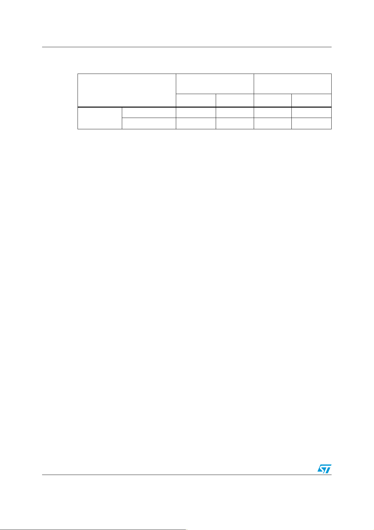
Table 1. dV/dt characterization @ 125 °C and V
device (I
dV/dt
(V/µs)
= 10 mA)
GT
Without gate to cathode
Sample 1 Sample 2 Sample 1 Sample 2
Direct 360 450 2260 1900
Reverse 800 760 800 760
Doc ID 022635 Rev 1 7/15
capacitor
= 402 V for sensitive Triac
peak
With gate to cathode
capacitor (100 nF)
Page 8
Gate to cathode capacitor, impact on dV/dt immunity AN4030
Table 2. dV/dt characterization @ 125 °C and V
device (I
dV/dt
(V/µs)
= 35 mA)
GT
Without gate to cathode
capacitor
Sample 1 Sample 2 Sample 1 Sample 2
Direct 2350 1850 2350 1850
Reverse 2750 1950 2750 1950
= 402 V for less sensitive Triac
peak
With gate to cathode
capacitor (100 nF)
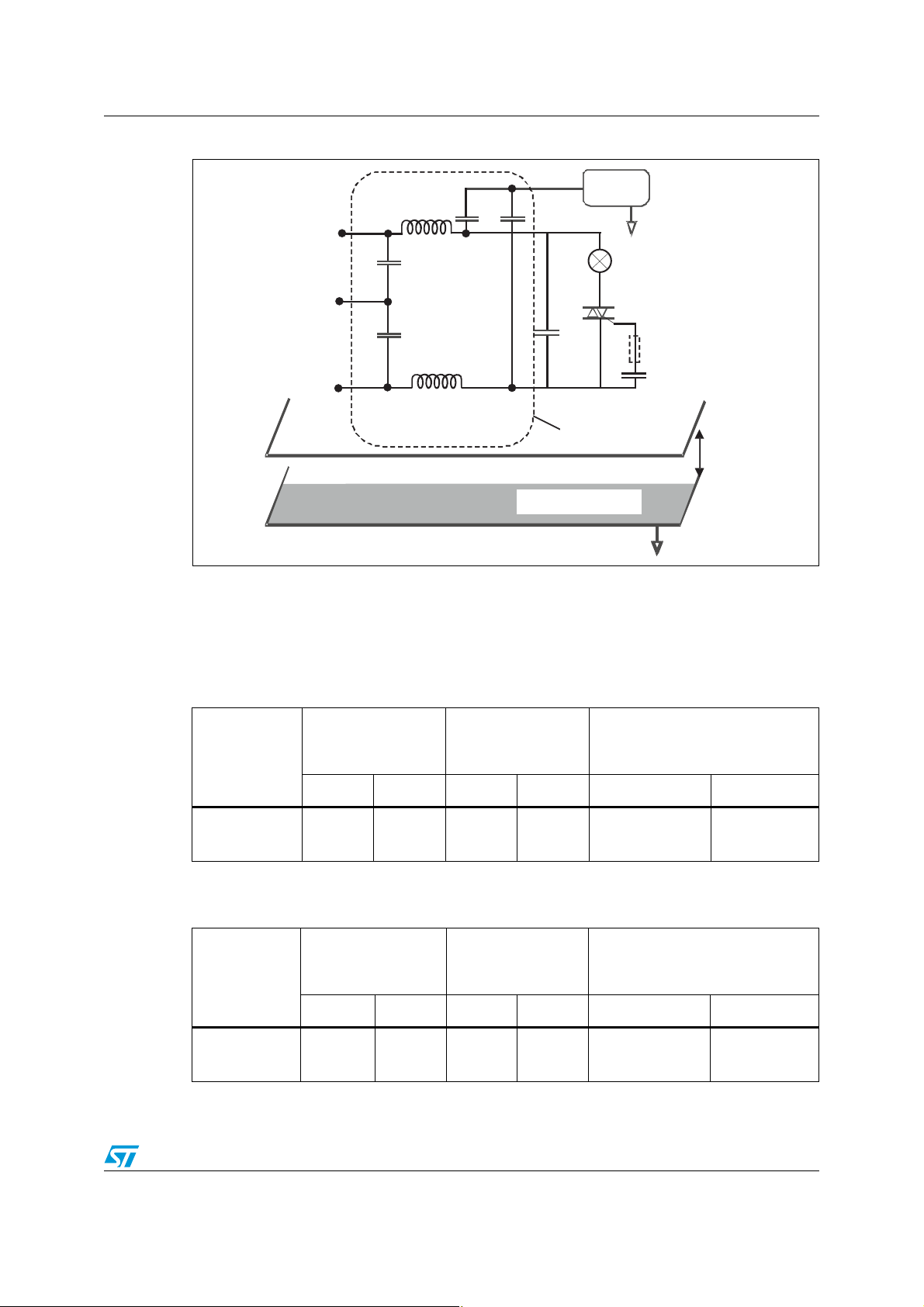
1.4 Behavior of Triacs to EFT (electrical fast transient)
To compare immunity between several Triacs (snubberless and logic level) with and without
gate to cathode capacitor, tests have been carried out in the following conditions (see
Figure 8):
● An X2 1nF capacitor is connected at line input.
● The PCB is 10 cm above the reference plane.
● The Triac A2 terminal is linked to a 25 W light bulb (resistive loads are chosen in order
to reduce dI/dt rates in case of firing).
● The gate could be left open, or connected to A1 terminal through an external gate to
cathode capacitor or connected to A1 through a 100 Ω R
cathode capacitor.
● No snubber circuits are added across the Triacs.
● Ambient temperature: 25 °C.
● The burst generator is programmed as required in the IEC 61000-4-4 standard (15 ms
burst duration, 3 Hz burst frequency, 5 kHz spike frequency, one second test duration).
in series with a gate to
G
8/15 Doc ID 022635 Rev 1
Page 9
AN4030 Gate to cathode capacitor, impact on dV/dt immunity
Figure 8. IEC 61000-4-4 test configuration
Burst
generator
L
PE
1 nF
X2
N
Coupling
network
Reference plane
R
G
C
GK
10 cm
PE
Ta bl e 3 and Ta bl e 4 give the test results for the two previous sample Triacs (logic level and
snubberless) with and without gate to cathode capacitor. A burst test is carried out for each
coupling mode (to line, to neutral, and to line and neutral). Only the minimum burst level
before turn-on, for all coupling modes, is recorded in these two tables.
Table 3. IEC 61000-4-4 tests results with logic level Triac - sensitive device
(I
= 10 mA)
GT
Without gate to
cathode capacitor
Sample 1 Sample 2 Sample 1 Sample 2 Sample 1 Sample 2
Minimum held
burst level (kV)
Table 4. IEC 61000-4-4 test results with snubberless Triac - less sensitive device
(I
1.3 1.3 3.6 3.5 3.3 3.2
= 35 mA)
GT
Without gate to
cathode capacitor
Sample 1 Sample 2 Sample 1 Sample 2 Sample 1 Sample 2
With gate to
cathode capacitor
(100 nF)
With gate to
cathode capacitor
(100 nF)
With R
With R
(100 Ω) and CGK (100 nF)
G
(100 Ω) and CGK (100 nF)
G
Minimum held
burst level (kV)
> 4.5 > 4.5 > 4.5 > 4.5 > 4.5 > 4.5
Doc ID 022635 Rev 1 9/15
Page 10

Gate to cathode capacitor, impact on dV/dt immunity AN4030
These experimental results show that there is no immunity improvement if a gate to cathode
capacitor is added to snubberless Triacs. Indeed, the immunity level is very high and above
our burst generator capability (4.5 kV).
On the other hand, logic level Triacs withstand a lower immunity level compared to
snubberless devices. This level is lower without gate to cathode capacitor. A 100 nF gate to
cathode capacitor improves almost by 3 the Triac immunity. But gate to cathode capacitor
lowers Triac reliability (refer to Section 2: Gate to cathode capacitor, impact on dI/dt
capability).
To keep the gate to cathode capacitor benefits without lowering system reliability, one
solution is then to add a resistor (R
) in series with gate to cathode capacitor. The immunity
G
level is then similar to that with the single gate to cathode capacitor. Such a resistor comes
for free, since the gate resistor, used to limit the control circuit output current, can be used
as R
.
G
Usually, logic level Triacs are driven directly by a microprocessor. MCU 4-4 immunity
behavior is improved by adding an RCR filter. A comparison with and without filter has been
performed with an ACST (I
max = 10 mA, 6 A on-state rms current) and an ST MCU. A
GT
capacitor is connected between 2 resistors and A1. One of these resistors (240 Ω) is
connected to the output of the MCU and the other one (50 Ω) to the ACST gate. This can
improve the level of immunity up to 600 V according to coupling, polarity and MCU output
configuration. For instance, with an MCU open drain output configuration, negative voltage
applied on Line, 4-4 immunity is 3.9 kV with a filter compared to 3.3 kV without a filter.
10/15 Doc ID 022635 Rev 1
Page 11

AN4030 Gate to cathode capacitor, impact on dI/dt capability
2 Gate to cathode capacitor, impact on dI/dt capability
As well as being almost ineffective in improving Triac immunity, a gate to cathode capacitor
has a major drawback when operating with Triacs. A gate to cathode capacitor significantly
decreases the Triac dI/dt capability. For example, Ta bl e 5 gives the experimental results
obtained in repetitive operation for a standard Triac (1 A, 600 V, 5 mA I
shows that the lifetime of the device is drastically reduced when a 100 nF or 10 nF gate to
cathode capacitor is added. On the other hand, the Triac dI/dt capability remains if a resistor
is added in series with a gate to cathode capacitor.
Table 5. Repetitive dI/dt tests results with a standard 1 A Triac
). Ta bl e 5 clearly
GT
Without gate to
cathode capacitor
dI/dt (A/µs) 30 30 30
I
(A) 3.5 3.5 3.5
peak
Number of cycles
(million of cycles)
Results 0 failed / 20 8 failed / 10 0 failed / 10
50 0.1 50
With gate to cathode
capacitor (100 nF)
With RG (50 Ω) and
(100 nF)
C
G
The high density current during charge and discharge of the capacitor explained the poor
life time with a gate to cathode capacitor. In case of an R
circuit, the resistor in series
G-CG
limited this density of current. Triac dV/dt immunity is improved with this circuit and dI/dt
capability is not decreased.
Figure 9 gives the different operating steps when a Triac is switched on in quadrant 2
(V
> 0 and IG < 0) with a gate to cathode capacitor.
T
The event sequence is as follows.
1. The triggering current is first sunk from the gate by the control circuit.
2. The pilot SCR is turned on. This pilot SCR is implemented by the P2-N2-P1-N4 layers.
It is not the same SCR that is on at the end of this switching-on process.
3. A high inrush current circulates through the gate to cathode capacitor due to the pilot
SCR turn-on (without gate to cathode capacitor, the gate current would be limited by
the gate resistor R
).
G
4. The gate to cathode capacitor is discharged after the main SCR turn-on. This SCR is
implemented by the P2-N2-P1-N1 layers. This causes a high peak gate current and
can damage the Triac.
Doc ID 022635 Rev 1 11/15
Page 12
Gate to cathode capacitor, impact on dI/dt capability AN4030
Figure 9. Sequence of events during Triac switch-on in quadrant 2
N1
P1
N2
P2
A1
3
I
C
C
GK
4
2
I
T
++
R
G
G
I
N4
A2
G
1
P1
N2
P2
N3
Even if the Triac is driven in zero voltage switch mode, a spurious turn-on could appear and
a high dI/dt could run through pilot SCR. A gate to cathode capacitor could increase the
failure rate as explained above. For example, for the sensitive logic level Triac described in
Section 1.4, non repetitive dI/dt capability robustness in Q2 is divided by around 2 with a
gate to cathode capacitor: 360 A/µS with C
= 200 nF and 670 A/µs without gate to
GK
cathode capacitor.
This behavior is not linked to the Triac technology but directly linked to the internal device.
So, whatever the technology, a gate to cathode capacitor will decrease dI/dt capability in
repetitive or in accidental mode.
12/15 Doc ID 022635 Rev 1
Page 13

AN4030 Conclusion
3 Conclusion
To increase power semiconductor device immunity to fast transient voltages it is quite
common to add a capacitor between the control terminal (gate or base) and the drive
reference terminal (source, emitter, cathode or A1 terminal). For SCRs, the drive reference
is the cathode, K. A gate to cathode capacitor is then usually added with very sensitive
devices and could be very useful to increase SCR immunity to dV/dt.
This Application note shows that as well as being almost ineffective in improving Triac
immunity, a gate to cathode capacitor has a major drawback when operating with Triacs.
Such a capacitor increases the failure rate when repetitive dI/dt rates are applied at turn-on
or in case of spurious turn-on with high dI/dt.
Explanations of silicon structure behavior during turn-on show the supplementary stress
due to a gate to cathode capacitor
capacitors should be removed from Triac designs.
irrespective of technology choice. This shows that such
Doc ID 022635 Rev 1 13/15
Page 14

Revision history AN4030
4 Revision history
Table 6. Document revision history
Date Revision Changes
27-Mar-2012 1 Initial release.
14/15 Doc ID 022635 Rev 1
Page 15

AN4030
Please Read Carefully:
Information in this document is provided solely in connection with ST products. STMicroelectronics NV and its subsidiaries (“ST”) reserve the
right to make changes, corrections, modifications or improvements, to this document, and the products and services described herein at any
time, without notice.
All ST products are sold pursuant to ST’s terms and conditions of sale.
Purchasers are solely responsible for the choice, selection and use of the ST products and services described herein, and ST assumes no
liability whatsoever relating to the choice, selection or use of the ST products and services described herein.
No license, express or implied, by estoppel or otherwise, to any intellectual property rights is granted under this document. If any part of this
document refers to any third party products or services it shall not be deemed a license grant by ST for the use of such third party products
or services, or any intellectual property contained therein or considered as a warranty covering the use in any manner whatsoever of such
third party products or services or any intellectual property contained therein.
UNLESS OTHERWISE SET FORTH IN ST’S TERMS AND CONDITIONS OF SALE ST DISCLAIMS ANY EXPRESS OR IMPLIED
WARRANTY WITH RESPECT TO THE USE AND/OR SALE OF ST PRODUCTS INCLUDING WITHOUT LIMITATION IMPLIED
WARRANTIES OF MERCHANTABILITY, FITNESS FOR A PARTICULAR PURPOSE (AND THEIR EQUIVALENTS UNDER THE LAWS
OF ANY JURISDICTION), OR INFRINGEMENT OF ANY PATENT, COPYRIGHT OR OTHER INTELLECTUAL PROPERTY RIGHT.
UNLESS EXPRESSLY APPROVED IN WRITING BY TWO AUTHORIZED ST REPRESENTATIVES, ST PRODUCTS ARE NOT
RECOMMENDED, AUTHORIZED OR WARRANTED FOR USE IN MILITARY, AIR CRAFT, SPACE, LIFE SAVING, OR LIFE SUSTAINING
APPLICATIONS, NOR IN PRODUCTS OR SYSTEMS WHERE FAILURE OR MALFUNCTION MAY RESULT IN PERSONAL INJURY,
DEATH, OR SEVERE PROPERTY OR ENVIRONMENTAL DAMAGE. ST PRODUCTS WHICH ARE NOT SPECIFIED AS "AUTOMOTIVE
GRADE" MAY ONLY BE USED IN AUTOMOTIVE APPLICATIONS AT USER’S OWN RISK.
Resale of ST products with provisions different from the statements and/or technical features set forth in this document shall immediately void
any warranty granted by ST for the ST product or service described herein and shall not create or extend in any manner whatsoever, any
liability of ST.
ST and the ST logo are trademarks or registered trademarks of ST in various countries.
Information in this document supersedes and replaces all information previously supplied.
The ST logo is a registered trademark of STMicroelectronics. All other names are the property of their respective owners.
© 2012 STMicroelectronics - All rights reserved
STMicroelectronics group of companies
Australia - Belgium - Brazil - Canada - China - Czech Republic - Finland - France - Germany - Hong Kong - India - Israel - Italy - Japan -
Malaysia - Malta - Morocco - Philippines - Singapore - Spain - Sweden - Switzerland - United Kingdom - United States of America
www.st.com
Doc ID 022635 Rev 1 15/15
 Loading...