

Page 1
Introduction
AM10219V1
AN4016
Application note
2 kW PPA for ISM applications
STMicoelectronics has recently introduced a new generation of high voltage DMOS
products housed in STAC
up to 1.2 kW for industrial, scientific, and medical applications such as 1.5 T and 3 T
magnetic resonance imaging (MRI). This new air-cavity technology now enables lower
thermal resistance, lower weight, and reduced cost compared to devices in ceramic
packages.
In this application note we report on the design of a 2 kW-100 V, 123 MHz Class AB peak
power amplifier (PPA) for 3 Tesla MRI applications. It almost doubles the output power of
previous amplifiers using MOSFET transistors in standard ceramic packages. The design
techniques and construction practices are described in enough detail to permit duplication
of the amplifier. The devices used in this amplifier are two STAC4932B N-channel
MOSFETs in a push-pull configuration capable of 1.2 kW each, under pulse conditions, and
housed in the STAC244B, a bolt-down air cavity package.
The design goals for the amplifier are:
■ Frequency: 123 MHz
■ Supply voltage: 100 V
■ Pulse conditions: 1 msec – 10%
■ Output power: > 2 kW
■ Gain: > 19 dB
■ Efficiency: > 60%
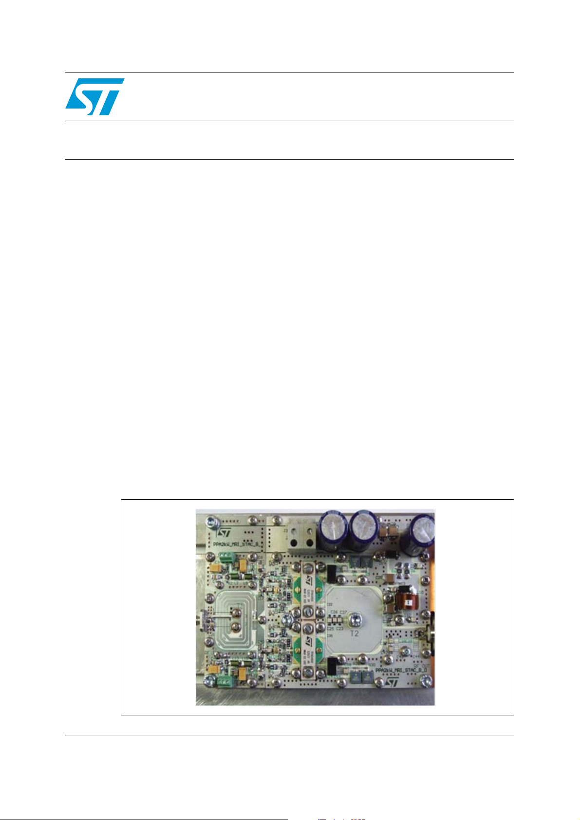
Figure 1. STEVAL-IMR002V1
®
air cavity packages and capable of delivering an output power of
December 2011 Doc ID 022523 Rev 1 1/17
www.st.com
Page 2

Contents AN4016
Contents
1 Design choices . . . . . . . . . . . . . . . . . . . . . . . . . . . . . . . . . . . . . . . . . . . . . 3
2 Circuit description . . . . . . . . . . . . . . . . . . . . . . . . . . . . . . . . . . . . . . . . . . . 5
3 Layout, parts list, and design considerations . . . . . . . . . . . . . . . . . . . . 7
4 MRI board performance and application . . . . . . . . . . . . . . . . . . . . . . . . 14
5 Conclusion . . . . . . . . . . . . . . . . . . . . . . . . . . . . . . . . . . . . . . . . . . . . . . . . 15
6 References . . . . . . . . . . . . . . . . . . . . . . . . . . . . . . . . . . . . . . . . . . . . . . . . 15
7 Revision history . . . . . . . . . . . . . . . . . . . . . . . . . . . . . . . . . . . . . . . . . . . 16
2/17 Doc ID 022523 Rev 1
Page 3
AN4016 Design choices
P1_RF INPUT
SMA_Female
P2_RF OUTPUT
N_Female
GND
GND
Q3
Q4
Q2
Q1
GND
GND
C31
C32
GND
R13
C9C14
GNDGND
+
C6
GND
C21
C40
R4
C18
R6
R8
R10
R12
R14
R15
C41
GND
R19
R20
R21
R25
R26
R27
GND
VCC
+
C13+C12
GNDGND
C23
C28
C30
GND
R17
R22
R3
Vg1
C34
C16
GND
+
C3
GNDGND
L2
C7
C10
GNDGND
+
C15
GND
R7
C8
C11
GNDGND
C17
STAC4932B
STAC4932B
T1
T2
L14
L3
R30
R1
C57
GND
GND
C58
L5
R24
Vg2
C48+C47
GNDGND
L13
C49
C52
GNDGND
+
C51
GND
R29
C50C53
GNDGND
L15
GND
L10
L8
L16
L12
L4
GND
C2
GND
R11
R16C24
GND
C20
C36
C45
R31
C55
GND
GND
GND
GND
GND
R28
R5
R9 GND
GND
C33
C37
C26C25
Rm
(~5 V typ)
(~5 V typ.)
(+100 V)
D1
LED
R32
GND
R33
GND
R34
R35
GND
C60
C59
C61
C63
C62
C64
VBIAS_1
VBIAS_1
VBIAS_1
VBIAS_2
VBIAS_2
VBIAS_2
GND
GND
Rm
GND
GND
C29
GND
GND
C42
J1
J2
J3
GND
Line_Bridge
GND
GND
1
2
3
CON3
1
2
3
CON3
Vg1
GND
GND
Vg2
1
CON11CON1
GND
Input Board 3 layer
Output Board 2 layer
C4
AM10220V1
1 Design choices
The main objectives of the 2 kW power amplifier design are board compactness (100 x 150
mm), full SMT technology, and to avoid the use of ferromagnetic components and coaxial
transmission line transformers.
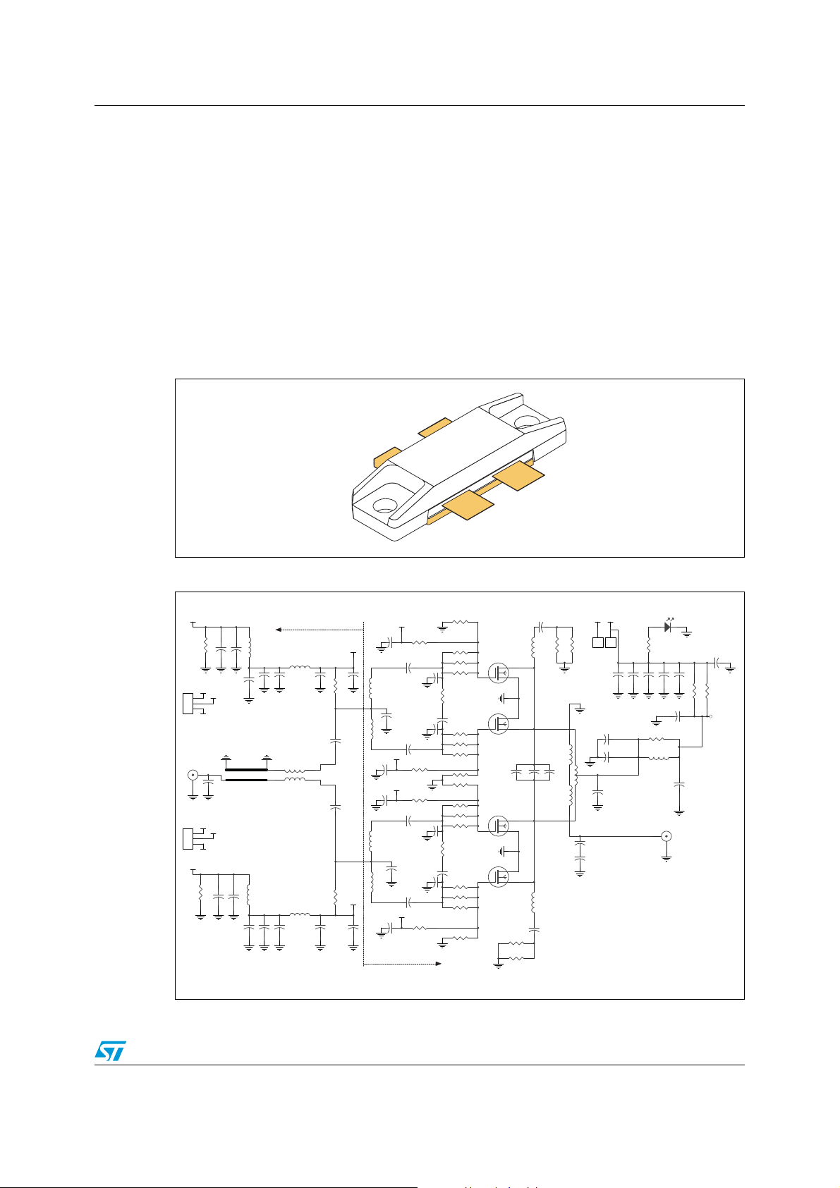
In summary, see circuit diagram in Figure 3, the power amplifier uses double push-pull boltdown devices, 2 x STAC4932B (see Figure 2) operate in Class AB. The two STACs are
driven in push-pull through the transformer T1 together with two in-phase power splitters:
this choice seems to be the best topology layout in terms of circuit size and mechanical
compactness. Moreover, as the temperature coefficient of MOSFET channel resistance is
positive, this makes a short-circuit possible in each pair of STAC4932B drains.
Figure 2. STAC244B bolt-down package
Figure 3. STEVAL-IMR002V1 circuit diagram
Doc ID 022523 Rev 1 3/17
Page 4

Design choices AN4016
Therefore, a compact design can be realized: only one RF output matching network, with
one impedance transformer T2, and an RF input matching network that supports the phase
and amplitude signals on each of the two gates STAC4932B (electrical symmetry).
The schematic incorporates the necessary input / output biasing networks for proper feed
biasing on the gates and drains.
Finally, planar microstrip technology was the main choice for the design of RF circuits: in
particular, the design of transformers T1 and T2 is fully embedded into the substrate (PCB)
itself as RF planar structures, and allows easy assembly of the design.
4/17 Doc ID 022523 Rev 1
Page 5

AN4016 Circuit description
2 Circuit description
The Input RF network must be carefully designed respecting the correct electrical symmetry,
because it is affected by driving high level signals (Pin ~ 20 W), and is made up of:
1. Balun transformer T1, λ / 4-25 Ohm transmission line type @ 123 MHz, needed to
lower the 50 Ohm RF input impedance to 12.5 Ohm, and is realized in a stripline
technique on a 2-layer substrate (Roger 4350B, with a thickness of 20 +20 mils: see
Figure 5) and is fed by a suspended microstrip line ('line bridge' in Figure 3). Moreover,
T1, being a quasi one-dimensional RF structure, can be mapped on the PCB without
compromising the electrical symmetry. T1, finally, is loaded from R7 and R29 in order to
dampen reflected waves from the gates and for stability purposes.
2. Two in-phase power splitters (L4, L8, C16, C18, C20) and (L12, L16, C36, C41, C45)
simply decrease the impedance level (2 Ohm), and more importantly, allow the gates of
each STAC4932 to be kept isolated.
3. RF decoupling filters, fed through the VG1 and VG2 connectors (Figure 3) need to bias
each STAC4932B gate. They are essentially LC multi-section filters with capacitors of
several technologies (tantalum, ceramic) to improve effective broadband RF isolation.
Independent voltage dividers act on the 4 gates (R4, R32, R16, R33, R17, R34, R31, R35)
to assure broadband RF stability, while the lower value series resistors (R6, R8, R10, ...)
need to dampen mismatching reflections on the gate impedance and then mitigate any
asymmetries on the gate impedance value.
The output RF network acts on the DMOS drains, in order to achieve optimal impedance by
means of the RF transformer T2, and also to properly feed high DC current filtered at
Vd=100 V, through the output biasing network directly via the primary winding of T2.
The transformer T2 (ratio 4:1) is designed on the top/bottom layers (see Figure 7) using
substrate Roger 4350B of 60 mils thickness in suspended broadside coupled strips and acts
as a composite transmission line transformer in balanced to unbalanced mode. The RF
output (type N-female connector) is directly connected to the winding output strip of T2 (see
top view in Figure 7) through an air suspended microstrip-line (50 Ohm): in this way, the
current (differential) generated on the primary winding strip (on the top layer) between the
two STACs is moved from T2 versus unbalanced RF output by the ground of the plate
copper carrier (see Figure 8) without further wave discontinuity, therefore avoiding losses
and creating a reliable design to support very high RF output power.
The transformer T2 has been designed using commercially available SW (ADS, HFSS) and
continues the refinement between electromagnetic and circuit simulation: T2, in fact, uses a
lamped capacitor (C25, C26, C23 caps group on winding top strip, and C37, C42 caps
group on the bottom side strip) to tune the proper impedance for DMOS drains.
In particular, the output biasing network (acts through the center tap of the winding top strip
of T2) uses several multilayer ceramic capacitors, and also adds the following electrical
functions:
1. Dampens voltage overshoot generated by each transient effected by pulsed RF
modulation: that is the group L10, R13, C29, C30, C33.
2. Two test points can be inserted between two calibrated Rm resistors for current /
voltage monitoring.
3. Lamp LED D1, for safety purposes.
Doc ID 022523 Rev 1 5/17
Page 6

Circuit description AN4016
Finally, the two bipole groups, consisting of L3-C37-R1/R5 and L14-C58-R28/R30, are
inserted in the drain side of the amplifier and give more flexibility to the impedence, for
example, it is used to improve low frequency stability, or to dominate harmonic impedance,
or as broadband internal RF loads.
6/17 Doc ID 022523 Rev 1
Page 7

AN4016 Layout, parts list, and design considerations
3 Layout, parts list, and design considerations
As mentioned previously (see Figure 3), the amplifier is built with separated input-output
PCB cards:
a) The input PCB, as shown in Figure 5, integrates the RF balun transformer, T1,
together with the RF decoupling networks.
b) The output PCB, see Figure 7, however, relates to the design of the RF
transformer, T2, with the remaining biasing/filtering networks for the gates and
drains of STAC4932B.
An image of the assembled board is shown in Figure 1, while Tabl e 1 gives the part list.
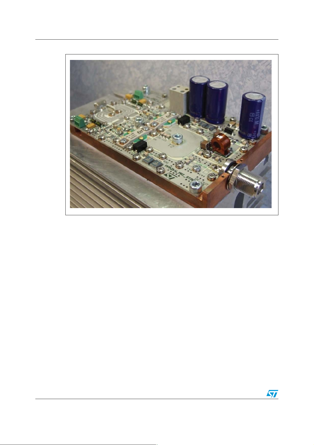
Figure 4, shows the final assembled board on the copper carrier and heatsink: board
robustness is an important factor in order to ensure electrical stability to manage very high
RF power.
The PCB cards are built in substrate Roger 4350B, in order to reduce dielectric losses
through the Joule effect (50 to 100 W less when compared to FR4 @ 2 kW), and in
particular to maintain thermal expansion compatibility with the copper carrier. Another
aspect of this rigid thermoset laminate allows the creation of a PCB with very good surface
finish, planarity and roughness, which are compatible with copper carrier surfaces that
support it. In fact, a carefully finished PCB surface is recommended: HAL LF with tinned
chemical deposition.
Moreover, accurate mounting procedures need to avoid bending/dirt that can compromise
the planarity of PCB cards.
Doc ID 022523 Rev 1 7/17
Page 8
Layout, parts list, and design considerations AN4016
AM10221V1
Figure 4. 2 kW MRI final assembled board
Figure 5 and Figure 7 show the input and output PCB cards, top and bottom-side. A
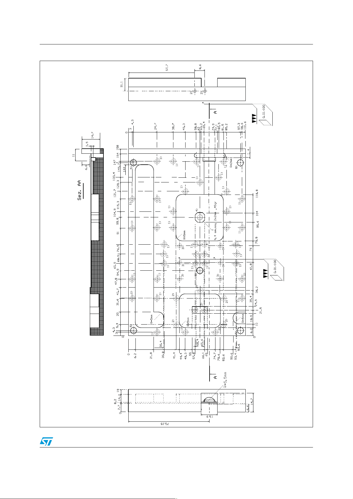
mechanical drawing of the base-plate is shown in Figure 8: in particular, the two
counterbores housing the transformers T1 and T2, are designed to control the unwanted
parasitic impedance (leakage) to ground.
8/17 Doc ID 022523 Rev 1
Page 9

AN4016 Layout, parts list, and design considerations
AM10222V1
Figure 5. Input PCB, and top and bottom view
The new package technology (STAC
®
) allows very low thermal impedance to be achieved,
Rtjc = 0.075 K / W (with T = 1 msec pulsed RF/Duty = 10%), so that, in combination with a
suitable heatsink (heatsink @ Rca <0.2 K / W max.), it permits the junction temperature to
be lower than the rating (Tjmax = 200 degC): in fact, considering a 60% efficiency @ 2200
W, a DeltaTjc = 56 ° C, and DeltaTca <15 ° C, a Tj=95 ° C max. junction temperature can be
expected.
The ability of STAC
®
to dissipate a high power pulse (see AN3232) allows the possibility to
reduce board dimension and external heatsinks; so that, using the flangeless package
STAC 244F (see Figure 6), you can design a new board with the same electrical
characteristics but with a dimension target of 80 x 100 mm.
Figure 6. STAC244B
Doc ID 022523 Rev 1 9/17
Page 10

Layout, parts list, and design considerations AN4016
AM10223v1
Figure 7. Output PCB, top and bottom view
Table 1. 2 kW MRI part list
Component ID Value Manufacturer Part code
C12, C13, C6 1000 µF, 100 V Panasonic ECA2AM102
C10, C11, C52, C53 100 nF Murata GCM188R71E104KA57D
C28 4.7 µF, 100 V TDK CKG57NX7R1E226M
C29 15 µF, 100 V Murata KRM552R72A156M
C15, C51 10 µF, 35 V KEMET T494D106K035AT
C3,C47 100 µF, 20 V KEMET T491X107K020AT
C4, C7, C48, C49 22 µF, 25 V Murata GRM32ER61E226ME15
C18, C41 300 pF ATC ATC100B301FWN200XC
C16, C20, C36, C45 68 pF ATC ATC800A680JTN250X
10/17 Doc ID 022523 Rev 1
Page 11

AN4016 Layout, parts list, and design considerations
Table 1. 2 kW MRI part list (continued)
Component ID Value Manufacturer Part code
C30 1000 pF ATC ATC100B102FWN300XC
C57, C58 3.3 pF ATC ATC100B3R3BW1500XT
C8, C31, C32, C50 470 pF ATC ATC 100B 471FWN200XC
C2, C17, C24, C34, C40, C55,
C59, C60, C61, C62, C63, C64
C9, C14 1 µF, 100 V AVX 22201C105KAT2A
C33 1 µF, 100 V AVX 12101C105K4Z2A
C21 18 pF ATC ATC100B180FWN1500XT
C25 75 pF ATC ATC100B750FWN1500XC
C26, C23 100 pF ATC ATC100B101FWN1500XC
C37, C42 56 pF ATC ATC100B560FWN1500XC
L10 700 nH Coilcraft CP-K0376-A
L2, L5, L13, L15 82 nH Coilcraft 1515SQ-82NJEB
L3, L14 110 nH Coilcraft 132-10SMJ
L4, L8, L12, L16 5.4 nH Coilcraft 0906-5JLB
R1, R5, R28, R30 50 Ω, 100 W Anaren C100N50Z4
R9 5600 Ω Tyco Electronics SMF25K6JT
R13 22 Ω Tyco Electronics SMW222RJT
R7, R29 100 Ω Panasonic ERJP14J101U
R11, R22 4.7 Ω Vishay 4.7 Ohm -1206
R3, R24 43 Ω Panasonic ERJP14J430U
2000 pF ATC ATC 200A202KTN50C
R32, R33, R34, R35 27 Ω Panasonic ERJP14J270U
R4, R16, R17, R31 20 Ω Panasonic ERJP14J200U
R6, R8, R10, R12, R14, R15, R19,
R20, R21,R25,R26, R27
Rm x 2 0.001 mΩ Tyco Electronics TL3A R001 1%
1P_J3 1 double pole Wieland 25.700.0153.0
Spacer_J3 Spacer Wieland 07.300.2753.0
3P_J1,J2 3 poles PHOENIX CONTACT 1725669
P2 N_Female Telegartner J01021A1084
P1 SMA_Female RADIALL R124.510.000W
(Q1-Q2)/(Q3-Q4) STAC4932B STMicroelectronics STAC4932B
D1 LED Kingbright KP-1608SURC
1 Ω Phycomp 232271111108
Doc ID 022523 Rev 1 11/17
Page 12

Layout, parts list, and design considerations AN4016
Table 2. Materials part list
Component Description
Line bridge
Board input
Fin fixing
Board output
Mechanical
plate
Roger 4350B, three layers, 20+20 mils, 1 OZ Cu on top-mid-bottom layers, Finit. metal HAL LF;
total Tk=1.2 mm max., top screen printing component, tin chemical surface deposition.
Roger 4350B, three layers, 20+20 mils, 1 OZ Cu on top-mid-bottom layers, Finit. metal HAL LF;
total Tk=1.2 mm max., top screen printing comp., tin chemical surface deposition.
Roger 4350B, two layers, Tk=60 mils, 1 OZ Cu on top- bottom layers, Finit. metal HAL LF; total
Tk=1.6 mm max., top screen printing comp., tin chemical surface deposition.
Roger 4350B, two layers, Tk=60 mils, 1 OZ Cu on top-bottom layers, Finit. metal HAL LF; total
Tk=1.6 mm max., top screen printing comp., tin chemical surface deposition.
PPAMRI_002-Rev B
12/17 Doc ID 022523 Rev 1
Page 13
AN4016 Layout, parts list, and design considerations
AM10224V2
Figure 8. Base-plate copper carrier
Doc ID 022523 Rev 1 13/17
Page 14

MRI board performance and application AN4016
-20
-18
-16
-14
-12
-10
-8
-6
-4
-2
0
5
7
9
11
13
15
17
19
21
23
25
105 110 115 120 125 130 135
IRL(dB
)
Gain(dB)
Freq(MHz
)
STAC4932B -
Gain & IRL Vs Freq @ Pin=43 dBm
PULSED WIDTH= 1msec, DUTYCYCLE =10%
Vds=100 VDC, Idq=2 x 100 mA
Gain
IRL
STAC244B
AM10225V1
4 MRI board performance and application
The power amplifier has been measured on two different RF scalar test benches: RF Power
Lab. in STM Catania (Italy) and RF Power Lab. in STM Quakertown (USA): the
measurements are in good agreement (+ / -0.15 dB max. error). The test includes a 2
kW/CW attenuator and a pulsed RF generator with high power amplifier driver to manage
large signals at RF input (20 W min.) with good harmonic rejection (-30 dBc).
Figure 9. Gain and IRL frequency response
Figure 9 shows the large signal gain frequency response of the amplifier, as well as the
input return loss, while Figure 10 shows the gain compression curve and the drain efficiency
curve Vs output power at 123 MHz (Idq = 200 mA and Vds = 100 V) and RF pulse width=1
msec, duty cycle=10%. The maximum efficiency is 60% @ 2.2 kW of output power.
14/17 Doc ID 022523 Rev 1
Page 15

AN4016 Conclusion
0
10
20
30
40
50
60
70
80
90
100
5
7
9
11
13
15
17
19
21
23
25
0 500 1000 1500 2000 2500
Drain Eff.(%)
Gain(dB)
Pout(W)
STAC4932B -
Gain & Eff. Vs Pout @ 123 MHz
PULSED WIDTH= 1msec, DUTYCYCLE =10%
Vds=100 VDC, Idq=2 x 100 mA
Gain
Eff.
AM10226V1
Figure 10. Gain and drain efficiency vs. output power
For IMS applications, two or more boards can be embedded to realize high power RF chains
(4 kW or more): e.g., 10 kW RF power can be obtained by linking six RF basic units,
properly using a Gysel power combiner, and integrated with the appropriate λ / 4
transmission lines to improve electrical stability, together with a control/monitoring card to
support global safety.
5 Conclusion
A pulsed RF high power amplifier (> 2 kW) has been described as a guideline-design,
oriented to new high voltage DMOS devices at Vd = 100 V: STAC4932B. In particular, the
amplifier combines excellent high frequency response with an efficient use of DC power and
allows a very compact design and robustness, in conjunction with SMT technology and
joined to the fully planar microstrip design (RF transformers). This amplifier can be
understood as the basic unit for high power RF chains to achieve very high power for an RF
pulse generator in the RF systems for medical magnetic resonance imaging (3T-fMRI).
6 References
● RF and Microwave Power Amplifier Design, by Andrei Grebennikov - Mc Graw Hill,
● Essentials of RF and Microwave Grounding, by Eric Holzman - Artech House, 2006
● AN3232 application note.
2005.
Doc ID 022523 Rev 1 15/17
Page 16

Revision history AN4016
7 Revision history
Table 3. Document revision history
Date Revision Changes
23-Dec-2011 1 Initial release.
16/17 Doc ID 022523 Rev 1
Page 17

AN4016
Please Read Carefully:
Information in this document is provided solely in connection with ST products. STMicroelectronics NV and its subsidiaries (“ST”) reserve the
right to make changes, corrections, modifications or improvements, to this document, and the products and services described herein at any
time, without notice.
All ST products are sold pursuant to ST’s terms and conditions of sale.
Purchasers are solely responsible for the choice, selection and use of the ST products and services described herein, and ST assumes no
liability whatsoever relating to the choice, selection or use of the ST products and services described herein.
No license, express or implied, by estoppel or otherwise, to any intellectual property rights is granted under this document. If any part of this
document refers to any third party products or services it shall not be deemed a license grant by ST for the use of such third party products
or services, or any intellectual property contained therein or considered as a warranty covering the use in any manner whatsoever of such
third party products or services or any intellectual property contained therein.
UNLESS OTHERWISE SET FORTH IN ST’S TERMS AND CONDITIONS OF SALE ST DISCLAIMS ANY EXPRESS OR IMPLIED
WARRANTY WITH RESPECT TO THE USE AND/OR SALE OF ST PRODUCTS INCLUDING WITHOUT LIMITATION IMPLIED
WARRANTIES OF MERCHANTABILITY, FITNESS FOR A PARTICULAR PURPOSE (AND THEIR EQUIVALENTS UNDER THE LAWS
OF ANY JURISDICTION), OR INFRINGEMENT OF ANY PATENT, COPYRIGHT OR OTHER INTELLECTUAL PROPERTY RIGHT.
UNLESS EXPRESSLY APPROVED IN WRITING BY TWO AUTHORIZED ST REPRESENTATIVES, ST PRODUCTS ARE NOT
RECOMMENDED, AUTHORIZED OR WARRANTED FOR USE IN MILITARY, AIR CRAFT, SPACE, LIFE SAVING, OR LIFE SUSTAINING
APPLICATIONS, NOR IN PRODUCTS OR SYSTEMS WHERE FAILURE OR MALFUNCTION MAY RESULT IN PERSONAL INJURY,
DEATH, OR SEVERE PROPERTY OR ENVIRONMENTAL DAMAGE. ST PRODUCTS WHICH ARE NOT SPECIFIED AS "AUTOMOTIVE
GRADE" MAY ONLY BE USED IN AUTOMOTIVE APPLICATIONS AT USER’S OWN RISK.
Resale of ST products with provisions different from the statements and/or technical features set forth in this document shall immediately void
any warranty granted by ST for the ST product or service described herein and shall not create or extend in any manner whatsoever, any
liability of ST.
ST and the ST logo are trademarks or registered trademarks of ST in various countries.
Information in this document supersedes and replaces all information previously supplied.
The ST logo is a registered trademark of STMicroelectronics. All other names are the property of their respective owners.
© 2011 STMicroelectronics - All rights reserved
STMicroelectronics group of companies
Australia - Belgium - Brazil - Canada - China - Czech Republic - Finland - France - Germany - Hong Kong - India - Israel - Italy - Japan -
Malaysia - Malta - Morocco - Philippines - Singapore - Spain - Sweden - Switzerland - United Kingdom - United States of America
www.st.com
Doc ID 022523 Rev 1 17/17
 Loading...