

Page 1
AN4015
Application note
Dual-BTL class-D audio amplifier demonstration board
based on the TDA7498E
Introduction
The purpose of this application note is to describe:
■ how to connect the TDA7498 demonstration board
■ how to evaluate the performance of the demonstration board using the electrical curves
■ how to avoid critical issues in the PCB schematic and layout of the TDA7498E
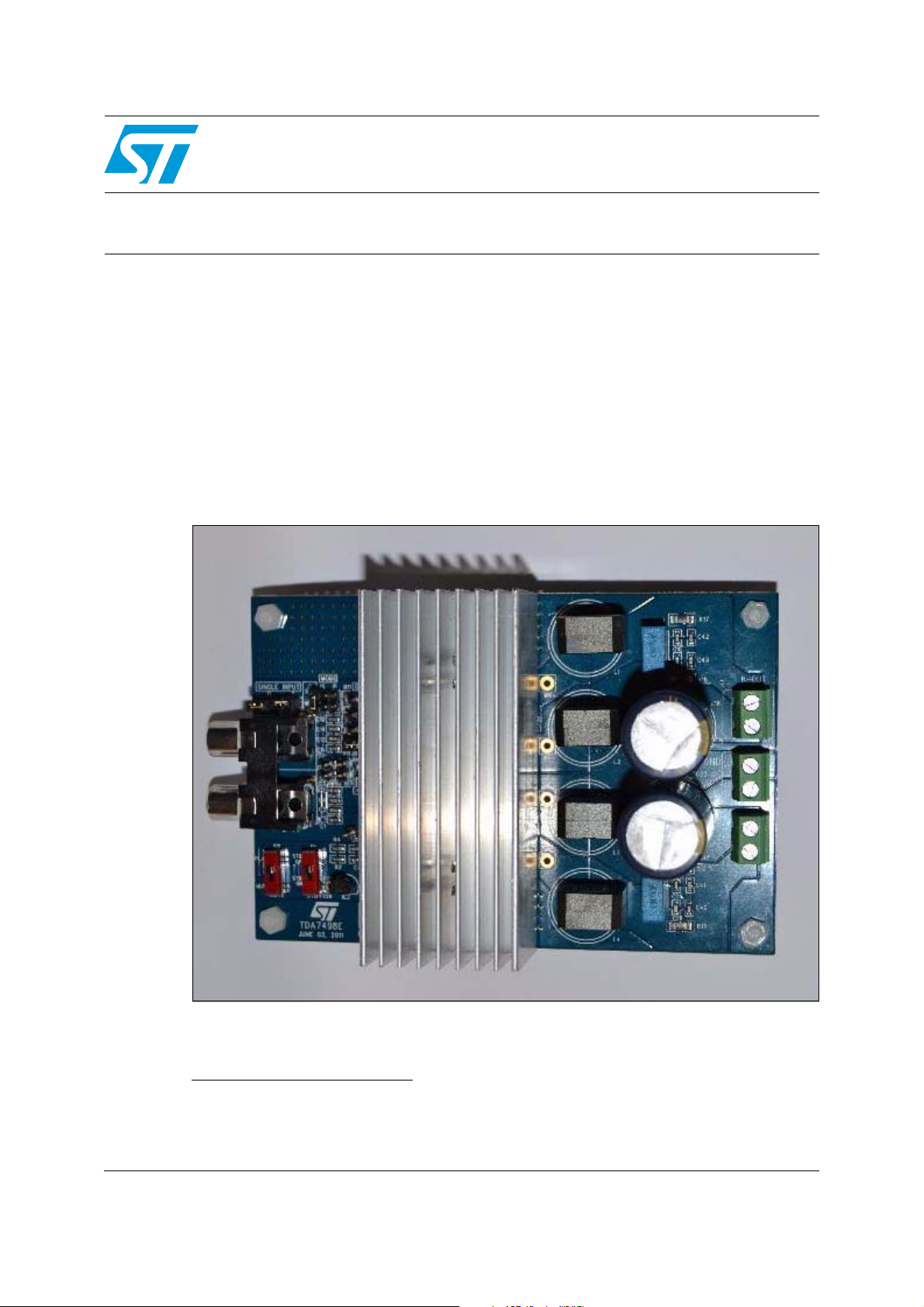
The TDA7498E represents a new generation of analog input class-D devices from
STMicroelectronics and is housed in a PSSO36 package. It is able to deliver 160 W +160 W
in stereo configuration with V
Figure 1. TDA7498E demonstration board
= 36 V and a 4 Ω load
CC
(a)
.
a. All of the results and graphs included in this document are measured using Audio Precision equipment.
January 2012 Doc ID 022507 Rev 1 1/22
www.st.com
Page 2

Contents AN4015
Contents
1 Overview . . . . . . . . . . . . . . . . . . . . . . . . . . . . . . . . . . . . . . . . . . . . . . . . . . 4
2 Test conditions and connections of the demonstration board . . . . . . . 5
2.1 Power supply and interface connection . . . . . . . . . . . . . . . . . . . . . . . . . . . 5
2.2 Output configuration . . . . . . . . . . . . . . . . . . . . . . . . . . . . . . . . . . . . . . . . . . 5
2.3 Connections . . . . . . . . . . . . . . . . . . . . . . . . . . . . . . . . . . . . . . . . . . . . . . . . 5
3 Schematic diagram and PCB layout . . . . . . . . . . . . . . . . . . . . . . . . . . . . 6
4 Electrical characteristics . . . . . . . . . . . . . . . . . . . . . . . . . . . . . . . . . . . . . 9
5 Test curves . . . . . . . . . . . . . . . . . . . . . . . . . . . . . . . . . . . . . . . . . . . . . . . 10
6 Design guidelines for PCB schematic and layout . . . . . . . . . . . . . . . . 14
6.1 Schematic . . . . . . . . . . . . . . . . . . . . . . . . . . . . . . . . . . . . . . . . . . . . . . . . . 14
6.1.1 Main driver for the selection of components . . . . . . . . . . . . . . . . . . . . . 14
6.1.2 Decoupling capacitors . . . . . . . . . . . . . . . . . . . . . . . . . . . . . . . . . . . . . . 14
6.1.3 Output filter . . . . . . . . . . . . . . . . . . . . . . . . . . . . . . . . . . . . . . . . . . . . . . 14
6.2 Layout . . . . . . . . . . . . . . . . . . . . . . . . . . . . . . . . . . . . . . . . . . . . . . . . . . . . 17
7 Revision history . . . . . . . . . . . . . . . . . . . . . . . . . . . . . . . . . . . . . . . . . . . 21
2/22 Doc ID 022507 Rev 1
Page 3

AN4015 List of figures
List of figures
Figure 1. TDA7498E demonstration board . . . . . . . . . . . . . . . . . . . . . . . . . . . . . . . . . . . . . . . . . . . . . 1
Figure 2. TDA7498E demonstration board connections . . . . . . . . . . . . . . . . . . . . . . . . . . . . . . . . . . . 5
Figure 3. TDA7498E schematic . . . . . . . . . . . . . . . . . . . . . . . . . . . . . . . . . . . . . . . . . . . . . . . . . . . . . . 6
Figure 4. PCB layout - top side . . . . . . . . . . . . . . . . . . . . . . . . . . . . . . . . . . . . . . . . . . . . . . . . . . . . . . 7
Figure 5. PCB layout - bottom side . . . . . . . . . . . . . . . . . . . . . . . . . . . . . . . . . . . . . . . . . . . . . . . . . . . 7
Figure 6. PCB layout - top and bottom sides plus components . . . . . . . . . . . . . . . . . . . . . . . . . . . . . . 8
Figure 7. THD+N vs. power . . . . . . . . . . . . . . . . . . . . . . . . . . . . . . . . . . . . . . . . . . . . . . . . . . . . . . . . 10
Figure 8. THD+N vs. frequency (ref = 1 W at 1 kHz) . . . . . . . . . . . . . . . . . . . . . . . . . . . . . . . . . . . . . 10
Figure 9. DNR . . . . . . . . . . . . . . . . . . . . . . . . . . . . . . . . . . . . . . . . . . . . . . . . . . . . . . . . . . . . . . . . . . 11
Figure 10. FFT (0 dBr at 1 W) . . . . . . . . . . . . . . . . . . . . . . . . . . . . . . . . . . . . . . . . . . . . . . . . . . . . . . . 11
Figure 11. Crosstalk . . . . . . . . . . . . . . . . . . . . . . . . . . . . . . . . . . . . . . . . . . . . . . . . . . . . . . . . . . . . . . . 12
Figure 12. Linearity . . . . . . . . . . . . . . . . . . . . . . . . . . . . . . . . . . . . . . . . . . . . . . . . . . . . . . . . . . . . . . . 12
Figure 13. Bandwidth . . . . . . . . . . . . . . . . . . . . . . . . . . . . . . . . . . . . . . . . . . . . . . . . . . . . . . . . . . . . . . 13
Figure 14. Pout vs. V
Figure 15. Snubber filter - solution 1 . . . . . . . . . . . . . . . . . . . . . . . . . . . . . . . . . . . . . . . . . . . . . . . . . . 15
Figure 16. Snubber filter - solution 2 . . . . . . . . . . . . . . . . . . . . . . . . . . . . . . . . . . . . . . . . . . . . . . . . . . 15
Figure 17. Dumping network . . . . . . . . . . . . . . . . . . . . . . . . . . . . . . . . . . . . . . . . . . . . . . . . . . . . . . . . 16
Figure 18. Frequency shift . . . . . . . . . . . . . . . . . . . . . . . . . . . . . . . . . . . . . . . . . . . . . . . . . . . . . . . . . . 16
Figure 19. Decoupling capacitors . . . . . . . . . . . . . . . . . . . . . . . . . . . . . . . . . . . . . . . . . . . . . . . . . . . . 17
Figure 20. Snubber network. . . . . . . . . . . . . . . . . . . . . . . . . . . . . . . . . . . . . . . . . . . . . . . . . . . . . . . . . 17
Figure 21. V
Figure 22. ROSC - component placement . . . . . . . . . . . . . . . . . . . . . . . . . . . . . . . . . . . . . . . . . . . . . . 18
Figure 23. Filter capacitors for SVR, VREF, SVCC, VSS and VDDPW. . . . . . . . . . . . . . . . . . . . . . . . 19
Figure 24. Input signal routing . . . . . . . . . . . . . . . . . . . . . . . . . . . . . . . . . . . . . . . . . . . . . . . . . . . . . . . 19
Figure 25. Signal ground and power ground routing . . . . . . . . . . . . . . . . . . . . . . . . . . . . . . . . . . . . . . 20
decoupling electrolytic capacitors . . . . . . . . . . . . . . . . . . . . . . . . . . . . . . . . . . . . . . . . 18
CC
and THD level . . . . . . . . . . . . . . . . . . . . . . . . . . . . . . . . . . . . . . . . . . . . . . . . 13
CC
Doc ID 022507 Rev 1 3/22
Page 4

Overview AN4015
1 Overview
The following terms used in this application note are defined as follows:
● THD+N vs. Pout: Total Harmonic Distortion (THD) plus noise versus output power
● THD+N vs. Freq: Total Harmonic Distortion plus noise versus frequency curve
● S/N Ratio: Signal-to-noise ratio
● DNR: Dynamic range
● FFT: Fast Fourier Transform Algorithm (method)
● XTalk: Channel separation L to R, or R to L channel crosstalk
The equipment used includes the following:
● Audio Precision 2722A + AES-17 filter + DCX+ AUX-0025 filter
● DC power supply
● Digital oscilloscope (Tektronix TDS5054B)
● Differential voltage probe (LeCroy AP031)
● Current probe (Tektronix TCP300)
Reference documents include:
● TDA7498E datasheet
● Schematic diagram
● PCB layout
● Te s t c u r ves
4/22 Doc ID 022507 Rev 1
Page 5
AN4015 Test conditions and connections of the demonstration board
2 Test conditions and connections of the
demonstration board
2.1 Power supply and interface connection
1. Connect PSU to the VCC terminal block
2. Connect the analog input cable to the RCA connectors on the demonstration board, the
other side must be connected to a signal source such as the Audio Precision analog
outputs or a DVD player
2.2 Output configuration
The TDA7498E demonstration board has been configured in 2-channel BTL output.
2.3 Connections
The board terminals (top view of demonstration board) are visible in Figure 2.
Figure 2. TDA7498E demonstration board connections
Left Load Right Load
Gain selection
Single-ended
input/differential
input mode
selection
Doc ID 022507 Rev 1 5/22
Analog input
Standby and mute
controls
Page 6
Schematic diagram and PCB layout AN4015
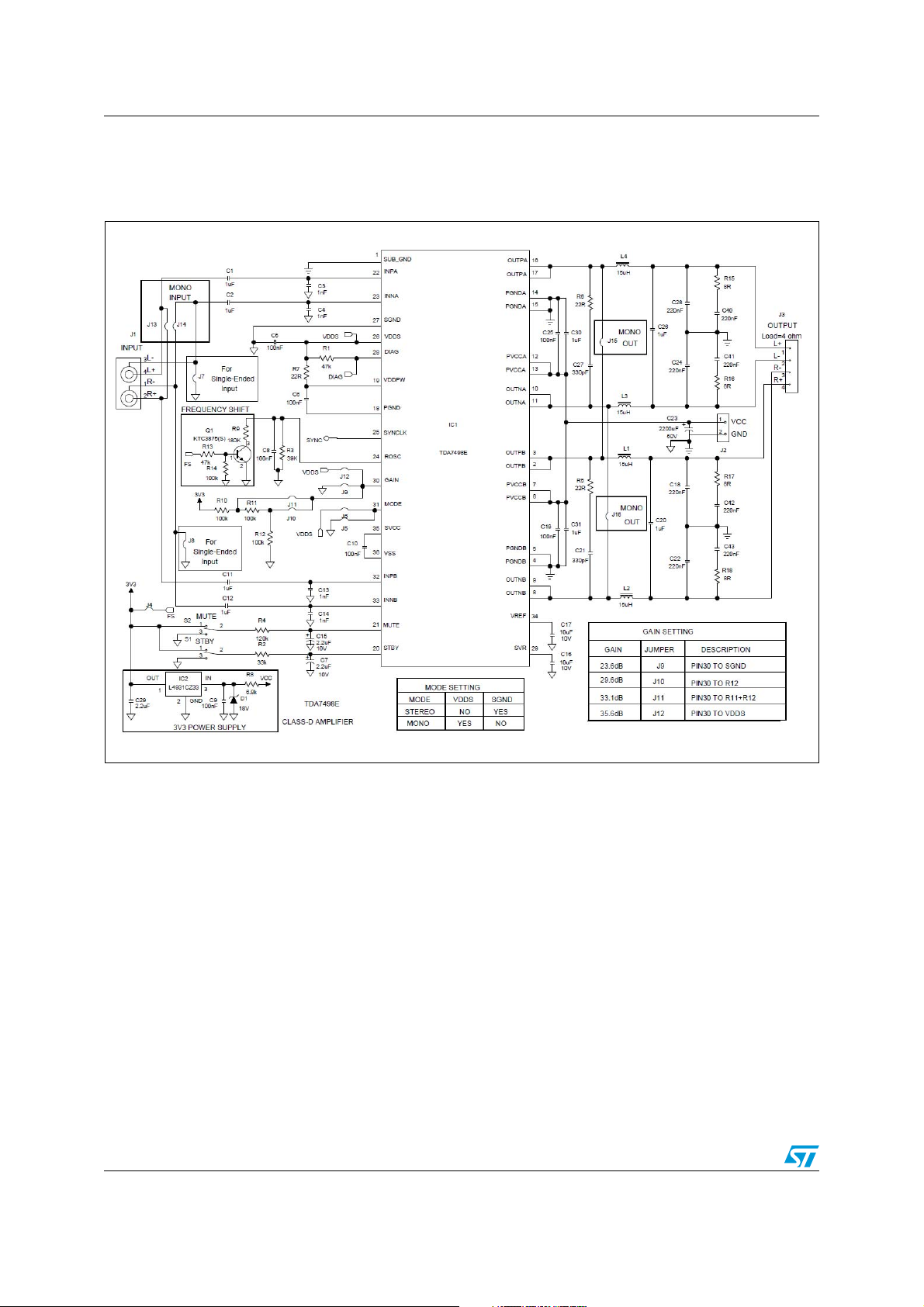
3 Schematic diagram and PCB layout
Figure 3. TDA7498E schematic
6/22 Doc ID 022507 Rev 1
Page 7
AN4015 Schematic diagram and PCB layout
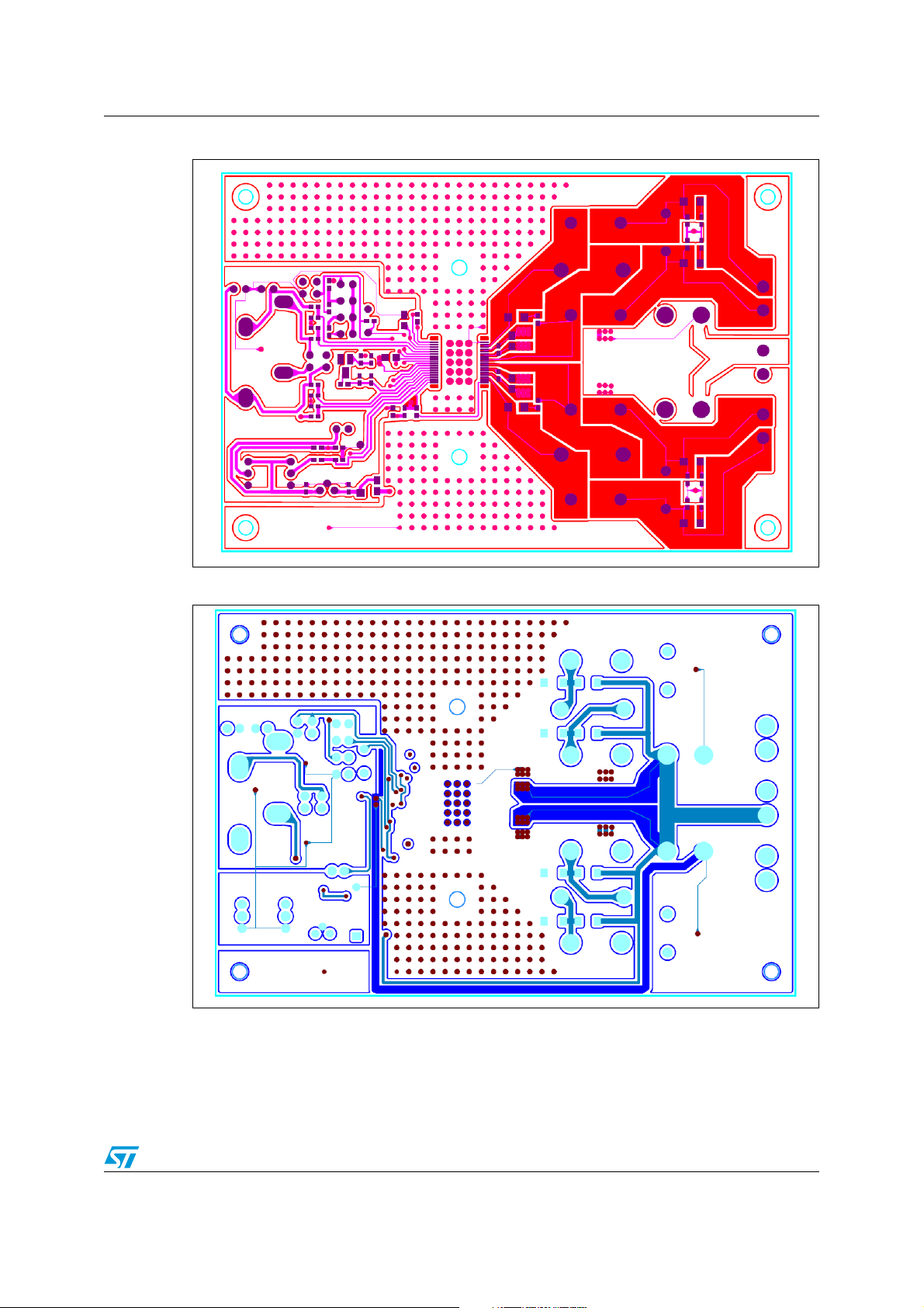
Figure 4. PCB layout - top side
Figure 5. PCB layout - bottom side
Doc ID 022507 Rev 1 7/22
Page 8

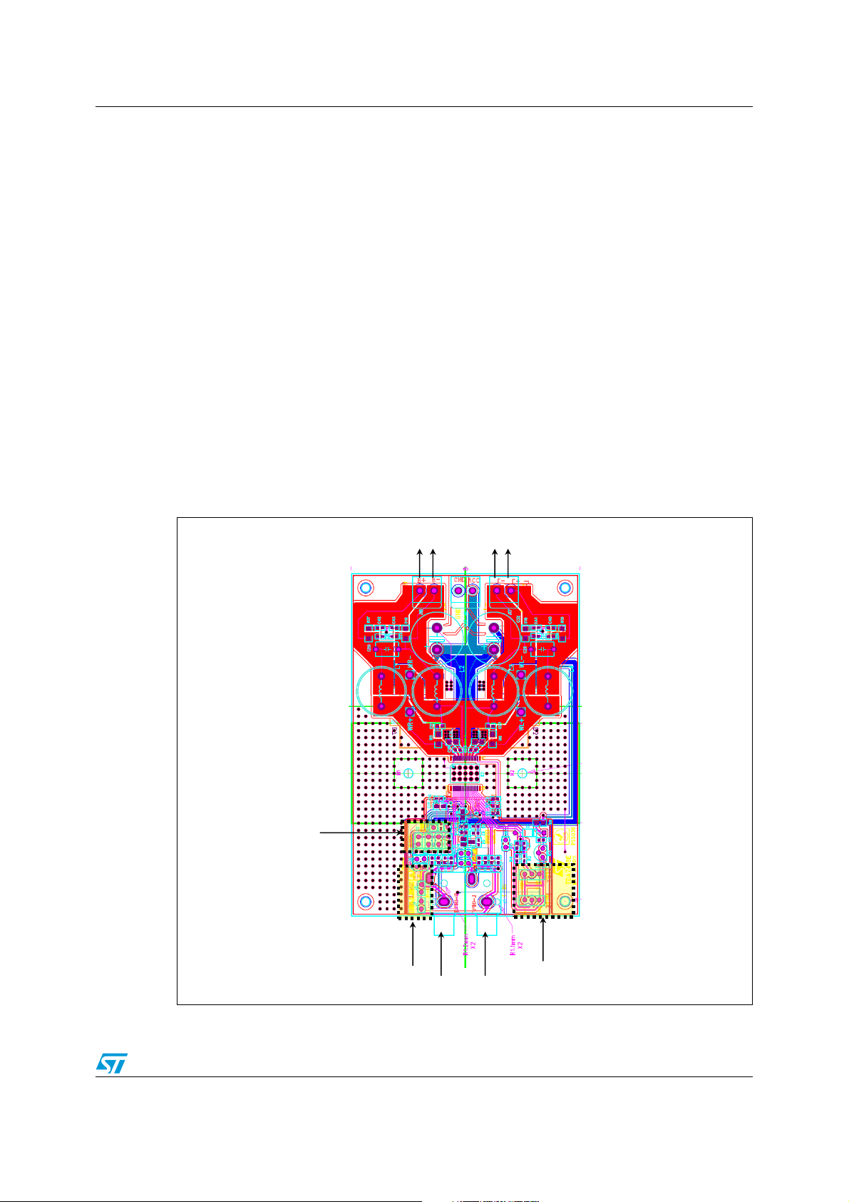
Schematic diagram and PCB layout AN4015
Figure 6. PCB layout - top and bottom sides plus components
8/22 Doc ID 022507 Rev 1
Page 9
AN4015 Electrical characteristics
4 Electrical characteristics
Referring to Figure 3: TDA7498E schematic, the Left (L) and Right (R) channels are the
output for a stereo configuration. V
InputFreq = 1 kHz; RefLevel = 1 W (0 dBr), Load = 4 Ω (resistive dummy load).
Table 1. Electrical characteristics
THD+N vs. power Pout = 1 W 0.0555%
I
OCP
SNR
DNR
Xtalk 1 kHz -85.9 dB
= +36 V, Gain 23.6 dB; Tamb = 25.5 °C;
CC
No filter -74.3 dB
AW - filter -77.5 dB
No filter -94 dB
AW - filter -98 dB
12 A
Doc ID 022507 Rev 1 9/22
Page 10

Test curves AN4015
5 Test curves
Figure 7. THD+N vs. power
10
5
2
1
0.5
%
0.2
0.1
0.05
0.02
0.01
1m 4002m 5m 10m 20m 50m 100m 500m 1 2 5 10 20 50 100 200
W
ColorSweep Tr ace Line Style Thi ck Dat a Axis Comment
1 1 Red Solid 2 Anlr.THD+N Ratio Left Vcc =36V; Load=4ohm; 1k Hz; Ch L
1 3 Blue Solid 2 Anlr.THD+N Ratio Left Vc c=36V; Load=4ohm; 1kHz; Ch R
Figure 8. THD+N vs. frequency (ref = 1 W at 1 kHz)
1
0.5
0.2
0.1
%
0.05
0.02
0.01
20 20k50 100 200 500 1k 2k 5k 10k
Hz
ColorSweep Tra ce Line Style Thi ck Data Axis Comment
1 1 Red Solid 2 Anlr.THD+N Ratio Left Vcc=36V; 1W@1kHz; Ch L
1 2 Blue Solid 2 Anlr.THD+N Ratio Left Vcc=36V; 1W@1kHz; Ch R
10/22 Doc ID 022507 Rev 1
Page 11
AN4015 Test curves
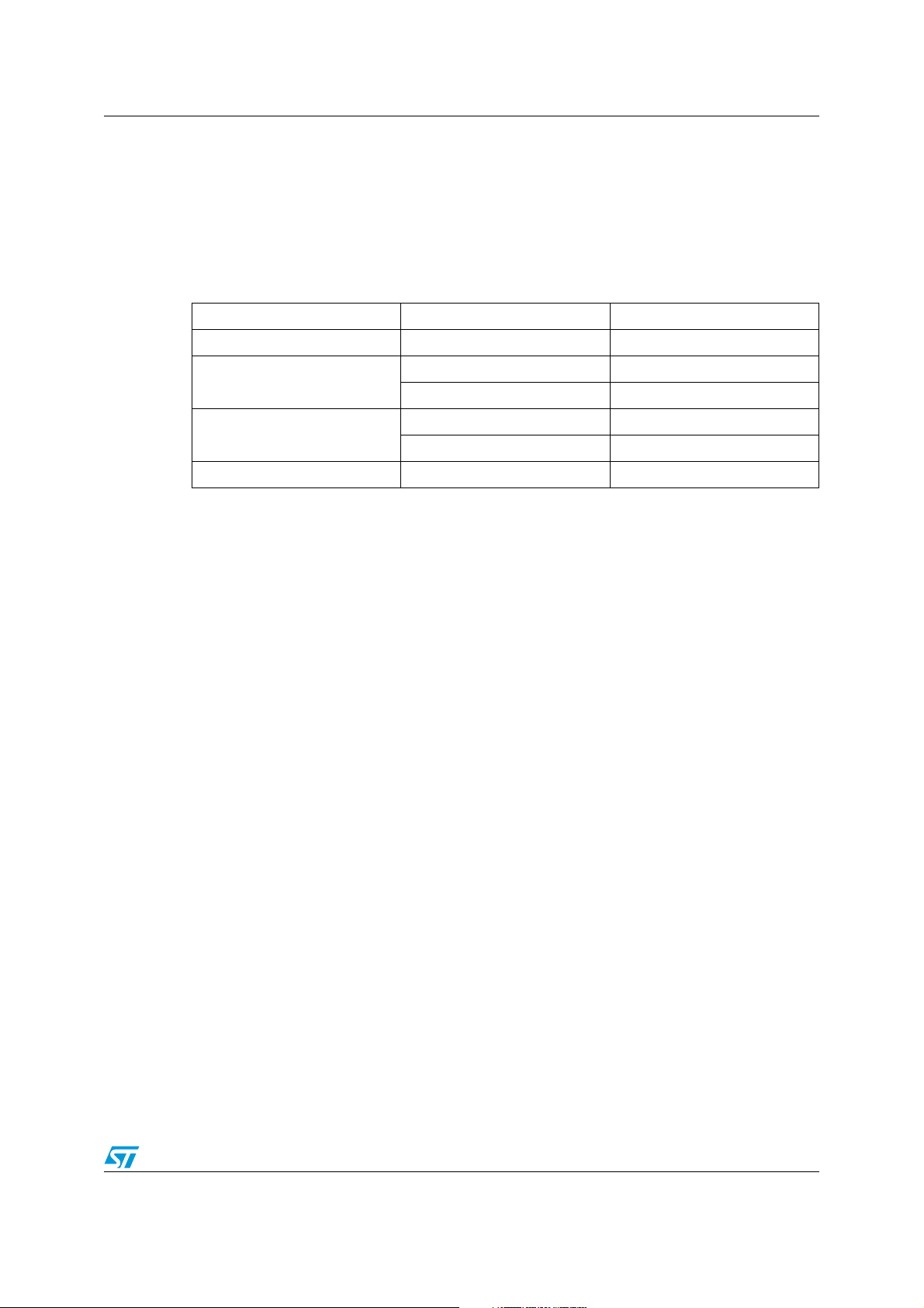
Figure 9. DNR
-20
-25
-30
-35
-40
-45
d
-50
B
-55
-60
-65
-70
-75
-80
-60 +0-55 -50 -45 -40 -35 -30 -25 -20 -15 -10 -5
dBr
ColorSweep Tra ce Line Style Thi ck Dat a Axis Comment
1 1 Red Solid 2 Anlr.THD+N Ratio Left Vc c=36V_1k Hz_4 ohm; Ch L
1 2 Blue Solid 2 Anlr.THD+N Ratio Left Vcc= 36V_1kHz_4 ohm ; Ch R
2 1 Green Solid 2 Anlr.THD+N Ratio Left Vcc=36V _1kHz _4 ohm; Ch R - A W Fi lter
2 2 Black Solid 2 Anlr.THD+N Ratio Left Vcc=36V_1k Hz_4 ohm; Ch L - AW Filt er
Figure 10. FFT (0 dBr at 1 W)
+0
-10
-20
-30
-40
-50
-60
d
B
-70
r
-80
A
-90
-100
-110
-120
-130
-140
-150
20 20k50 100 200 500 1k 2k 5k 10k
ColorSweep Tra ce Line Sty le Thi ck Data Axis Com ment
1 1 Red Solid 2 Fft.Ch.1 Ampl Left Vcc=36V; Ref: 1W@1kHz: Ch L
1 2 Blue Solid 2 Fft.Ch.2 Ampl Right Vcc=36V; Ref: 1W@1kHz : Ch R
+0
-10
-20
-30
-40
-50
-60
d
B
-70
r
-80
B
-90
-100
-110
-120
-130
-140
-150
Hz
Doc ID 022507 Rev 1 11/22
Page 12
Test curves AN4015
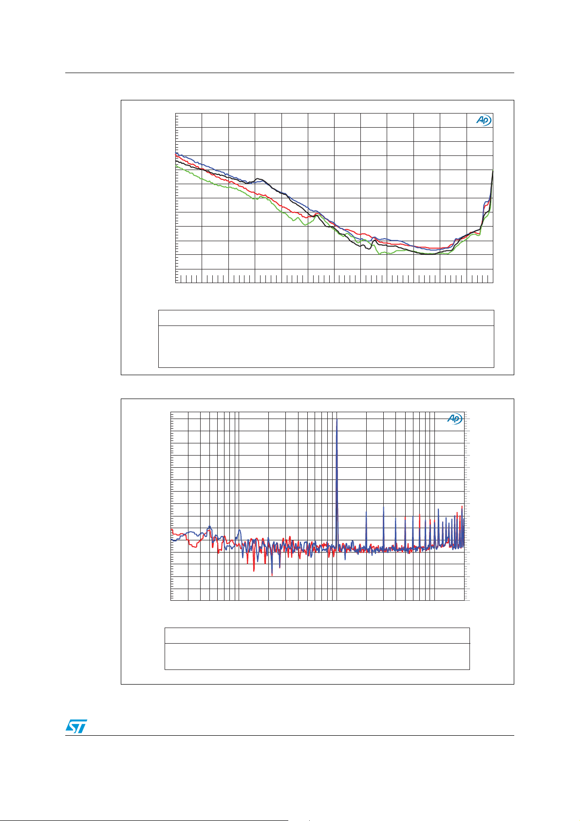
Figure 11. Crosstalk
+0
-10
-20
-30
-40
-50
d
-60
B
-70
-80
-90
-100
-110
-120
20 20k50 100 200 500 1k 2k 5k 10k
Hz
ColorSweep Tr ace Line S tyle Thic k Data Axis Comment
1 1 Red Solid 2 S2C.Anlr.Crosstalk Left Vcc= 36V; 1W ; 4ohm; (Ch L on)
1 2 Blue Solid 2 S2C.Anlr.Crosstalk Left Vcc =36V; 1W ; 4ohm; (Ch R on)
Figure 12. Linearity
24
23.5
23
22.5
22
Gain [dB]
21.5
21
20.5
Left
20
0 0. 2 0.4 0.6 0.8 1 1.2 1.4 1.6 1.8 2
Right
Gain Linearity
Input Level [V]
12/22 Doc ID 022507 Rev 1
Page 13
AN4015 Test curves
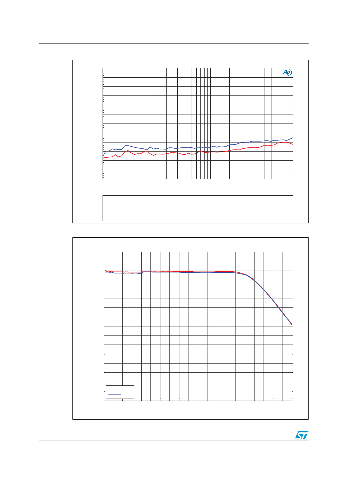
Figure 13. Bandwidth
+1
+1
+0.5
+0
-0.5
d
B
-1
r
A
-1.5
-2
-2.5
-3
10 50k20 50 100 200 500 1k 2k 5k 10k 20k
1 1 Red Solid 2 Anlr.Level A Left Vcc=36V; 1W; Ch L
1 2 Blue Solid 2 Anlr.Level B Right Vcc=36V; 1W; Ch R
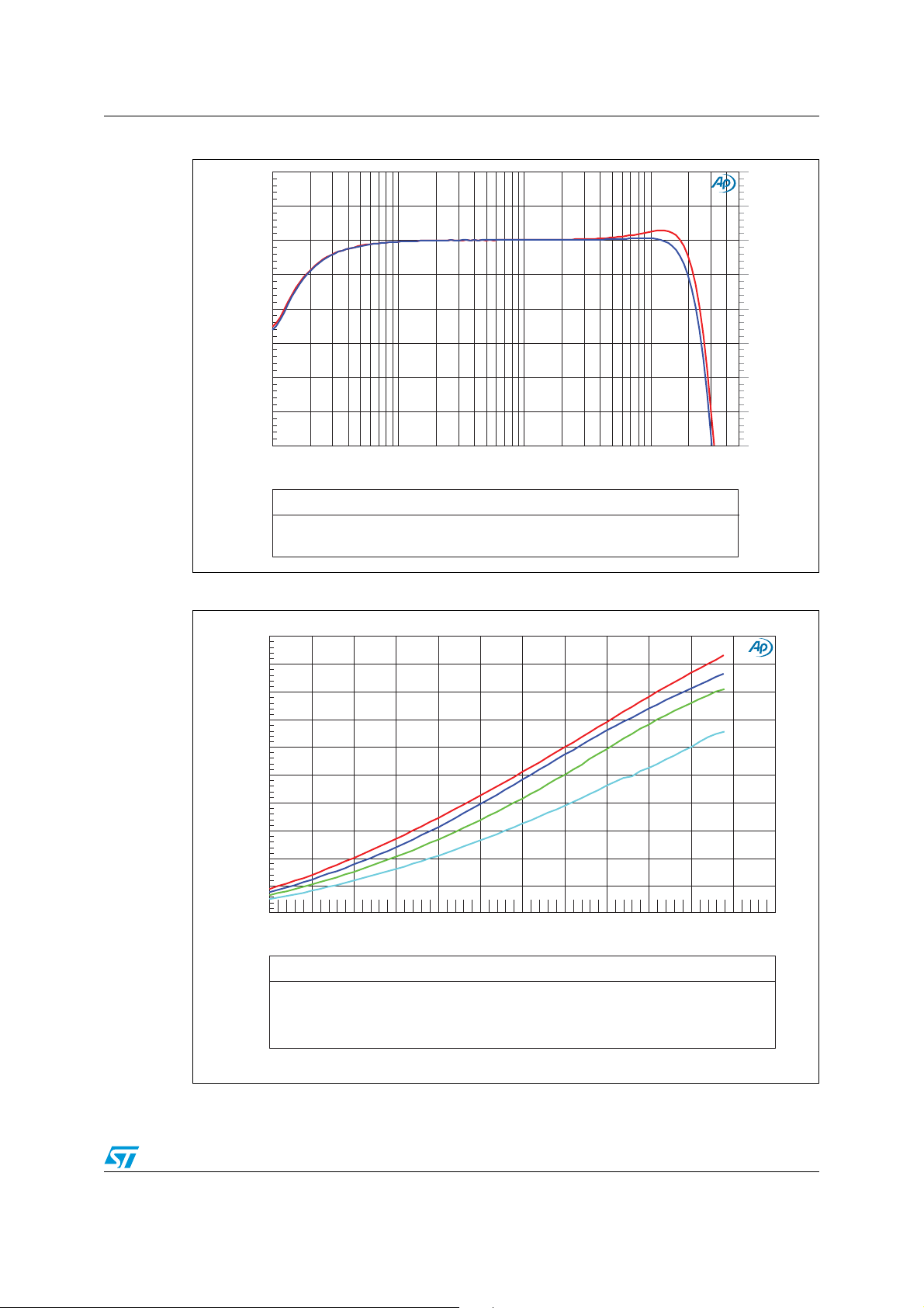
Figure 14. Pout vs. V
200
180
Hz
ColorSweep Tra ce Line Style Th ic k Dat a Axis Comment
and THD level
CC
+0.5
+0
-0.5
-1
-1.5
-2
-2.5
-3
d
B
r
B
160
140
120
100
W
80
60
40
20
+10 +40+12.5 +15 +17.5 +20 +22.5 +25 +27.5 +30 +32.5 +35 +37.5
Vdc
ColorSweep Tra ce Line Style Th ic k Data Axis Comment
1 1 Cy an Solid 2 Anlr.Level A Left Pout vs. Vc c; Load=4ohm ; THD=1%
2 1 Green Solid 2 Anlr.Level A Left Pout vs. Vc c; Load=4ohm ; THD=10%
3 1 Blue Solid 2 Anlr.Level A Left Pout vs. Vc c; Load= 4ohm; THD=20%
4 1 Red Solid 2 Anlr.Level A Left Pout vs. Vc c; Load=4ohm; THD=30%
Doc ID 022507 Rev 1 13/22
Page 14

Design guidelines for PCB schematic and layout AN4015
6 Design guidelines for PCB schematic and layout
6.1 Schematic
6.1.1 Main driver for the selection of components
● Absolute maximum rate (input V
● Bypass capacitor 100 nF in parallel to 1µF for each power V
is suggested.
● Coil saturation current must be compatible with the peak current of application
6.1.2 Decoupling capacitors
There are two different ways to use the decoupling capacitors:
● The decoupling capacitor(s) can be shared among channels; the layout must be
designed to implement a "star route" for the V
● One decoupling capacitor can be used for each channel. It is mandatory that each
decoupling capacitor be placed as close as possible to the IC pins. This solution is
implemented on the TDA7498E demonstration board.
6.1.3 Output filter
● Snubber network: the key function of a snubber network is to absorb energy from the
inductive component in the power circuit (the output coils and the speaker). The
purpose of the snubber RC network is to dissipate the unnecessary high pulse energy,
such as a high voltage spike, in the power circuit which is dangerous to the system.
● Main filter (low-pass filter): The purpose of the main filter is to remove the carrier
frequency (≈310 kHz) and to cut off the frequency higher than the audible range of
20 kHz. The LPF filter is implemented by a passive Butterworth topology. In order to
have a clean and flat frequency response, it is mandatory to design the filter to fix the
cutoff frequency a little bit above 20 kHz.
● Damping network: The purpose of the damping network is to avoid the high-frequency
oscillation issue on the output circuit. When the load is disconnected from the amplifier,
the frequency response of the main filter is not flat and there is the possibility of adding
gain in a frequency band. The damping network also improves the THD performance.
The damping network can also avoid the inductive effect of the PCB tracks when the
system is working at high frequency with PWM.
supply): 40 V
CC
CC
paths.
branch. Dielectric X7R
CC
14/22 Doc ID 022507 Rev 1
Page 15

AN4015 Design guidelines for PCB schematic and layout
Snubber filter
The snubber circuit must be optimized for the specific application. Starting values are
330 pF in series to 22 ohm. The power dissipation of this network (resistor) depends on the
power supply, frequency and capacitor values using following formula:
PCf2V⋅()
⋅⋅=
2
This power is dissipated on the series resistance.
Figure 15. Snubber filter - solution 1
INxA
C126
330p
R44
22
INxB
To increase the efficiency, it is possible to use two equal snubber networks toward GND. In
this case, the formula to evaluate power is:
PCf2V
This power is dissipated on the resistance.
Figure 16. Snubber filter - solution 2
INxA
⋅⋅ ⋅=
C127
330p
R45
22
R46
22
2
C130
INxB
Doc ID 022507 Rev 1 15/22
330p
Page 16

Design guidelines for PCB schematic and layout AN4015
Dumping network
The C-R-C is a dumping network. It is mainly intended for high inductive loads and for
common-mode noise attenuation.
Figure 17. Dumping network
PWM output frequency shifting for AM band radio sensitivity improvement
Using a logic control signal (FS) from MCU or from a DSP (3.3 V) it is possible to modify the
PWM output frequency.
Figure 18. Frequency shift
(b)
b. For the PWM frequency calculation formula please refer to the datasheet.
16/22 Doc ID 022507 Rev 1
Page 17

AN4015 Design guidelines for PCB schematic and layout
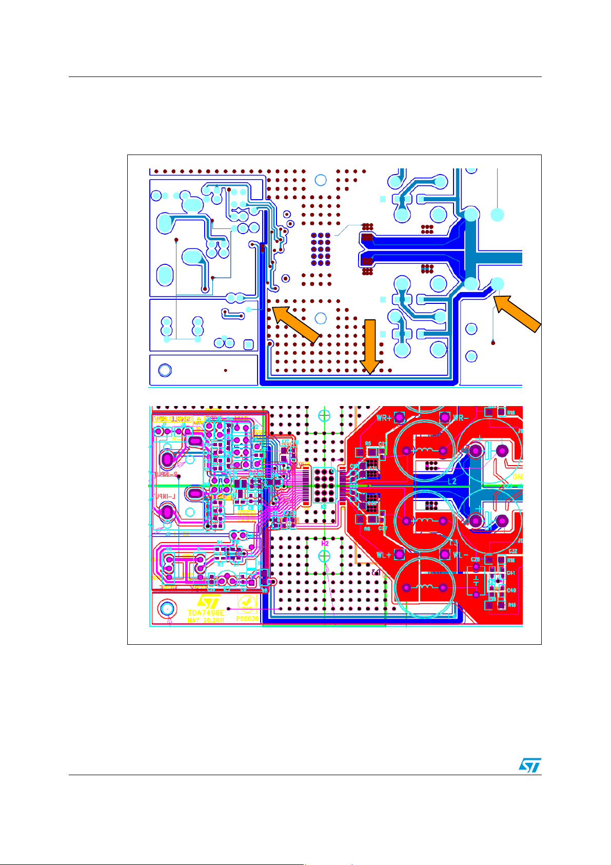
6.2 Layout
● Solder 100 nF and 1µF bypass ceramic capacitors as close as possible to the related
IC pin
● To avoid the effect due to the parasitic inductive coil generated by the copper wires, it is
suggested to use the ceramic capacitor to balance the reactance. It's mandatory to
place the ceramic capacitor as close as possible to the related pins. The distance
between the capacitor to the related pins is recommended to be within 5 mm.
Figure 19. Decoupling capacitors
Ground pin and Vcc pin of
100 nF and 1μF capacitors
should be connected to the
related IC pin directly
● Solder the snubber networks as close as possible to the related IC pin. A high level
spike may occur if the snubber network is placed too far from the pins. It's
recommended that the distance from the snubber network be within 3 mm which takes
into consideration the width of the copper wire.
Figure 20. Snubber network
Snubber network
Doc ID 022507 Rev 1 17/22
Page 18

Design guidelines for PCB schematic and layout AN4015
Figure 21. V
● Use electrolytic capacitors first to separate the V
branches. A "star route" for the VCC
CC
supply is suggested to avoid interference between the channels such as when one
channel is idle while the other channel is working with a full load. In applications with
high output power, another approach is to filter the two channels separately. This
solution is implemented in this demonstration board.
decoupling electrolytic capacitors
CC
● ROSC network: Place the RC filter for the ROSC pin close to the IC
Figure 22. ROSC - component placement
R-C network for
ROSC
18/22 Doc ID 022507 Rev 1
Page 19

AN4015 Design guidelines for PCB schematic and layout
● Place the filter capacitors for SVR, VREF, SVCC, VSS and VDDPW close to the IC.
Figure 23. Filter capacitors for SVR, VREF, SVCC, VSS and VDDPW
Filter capacitors for
VREF, SVCC and
VSS
Filter capacitor for SVR
Filter capacitors
for VDDS and
VDDPW
● Input signal routing
Figure 24. Input signal routing
Doc ID 022507 Rev 1 19/22
Page 20
Design guidelines for PCB schematic and layout AN4015
● Signal ground and power ground routing: the signal ground should be connected to the
bulk capacitor negative terminal via a dedicated copper track; no vias must be present
in the connection path.
Figure 25. Signal ground and power ground routing
20/22 Doc ID 022507 Rev 1
Page 21

AN4015 Revision history
7 Revision history
Table 2. Document revision history
Date Revision Changes
09-Jan-2012 1 Initial release.
Doc ID 022507 Rev 1 21/22
Page 22

AN4015
Please Read Carefully:
Information in this document is provided solely in connection with ST products. STMicroelectronics NV and its subsidiaries (“ST”) reserve the
right to make changes, corrections, modifications or improvements, to this document, and the products and services described herein at any
time, without notice.
All ST products are sold pursuant to ST’s terms and conditions of sale.
Purchasers are solely responsible for the choice, selection and use of the ST products and services described herein, and ST assumes no
liability whatsoever relating to the choice, selection or use of the ST products and services described herein.
No license, express or implied, by estoppel or otherwise, to any intellectual property rights is granted under this document. If any part of this
document refers to any third party products or services it shall not be deemed a license grant by ST for the use of such third party products
or services, or any intellectual property contained therein or considered as a warranty covering the use in any manner whatsoever of such
third party products or services or any intellectual property contained therein.
UNLESS OTHERWISE SET FORTH IN ST’S TERMS AND CONDITIONS OF SALE ST DISCLAIMS ANY EXPRESS OR IMPLIED
WARRANTY WITH RESPECT TO THE USE AND/OR SALE OF ST PRODUCTS INCLUDING WITHOUT LIMITATION IMPLIED
WARRANTIES OF MERCHANTABILITY, FITNESS FOR A PARTICULAR PURPOSE (AND THEIR EQUIVALENTS UNDER THE LAWS
OF ANY JURISDICTION), OR INFRINGEMENT OF ANY PATENT, COPYRIGHT OR OTHER INTELLECTUAL PROPERTY RIGHT.
UNLESS EXPRESSLY APPROVED IN WRITING BY TWO AUTHORIZED ST REPRESENTATIVES, ST PRODUCTS ARE NOT
RECOMMENDED, AUTHORIZED OR WARRANTED FOR USE IN MILITARY, AIR CRAFT, SPACE, LIFE SAVING, OR LIFE SUSTAINING
APPLICATIONS, NOR IN PRODUCTS OR SYSTEMS WHERE FAILURE OR MALFUNCTION MAY RESULT IN PERSONAL INJURY,
DEATH, OR SEVERE PROPERTY OR ENVIRONMENTAL DAMAGE. ST PRODUCTS WHICH ARE NOT SPECIFIED AS "AUTOMOTIVE
GRADE" MAY ONLY BE USED IN AUTOMOTIVE APPLICATIONS AT USER’S OWN RISK.
Resale of ST products with provisions different from the statements and/or technical features set forth in this document shall immediately void
any warranty granted by ST for the ST product or service described herein and shall not create or extend in any manner whatsoever, any
liability of ST.
ST and the ST logo are trademarks or registered trademarks of ST in various countries.
Information in this document supersedes and replaces all information previously supplied.
The ST logo is a registered trademark of STMicroelectronics. All other names are the property of their respective owners.
© 2012 STMicroelectronics - All rights reserved
STMicroelectronics group of companies
Australia - Belgium - Brazil - Canada - China - Czech Republic - Finland - France - Germany - Hong Kong - India - Israel - Italy - Japan -
Malaysia - Malta - Morocco - Philippines - Singapore - Spain - Sweden - Switzerland - United Kingdom - United States of America
www.st.com
22/22 Doc ID 022507 Rev 1
 Loading...