

AN4007
Application note
EVLVIP37LE5V3A: 15 W (5 V - 3 A) wide range single-output
demonstration board
By Fabio Cacciotto
Introduction
In several applications, such as LCD or plasma TVs, desktop computers, etc., the power
supply that converts the energy from the main, often includes two modules: the main power
supply that provides most of the power and is OFF when the application is OFF or in
standby mode, and the auxiliary power supply that provides energy only to some specific
parts of the equipment such as USB ports, remote receivers, or modems but is still ON
when the application is in standby mode.
It is often required that, in standby condition, the equipment input power is as low as
possible which means the input power of the auxiliary power supply in no load or light load
condition is reduced as low as possible.
This application note introduces a new offline high voltage converter from the VIPerPlus
family, the VIPER37LE and the presented demonstration board meets the specifications of a
wide range of auxiliary power supplies for said applications. Furthermore, it is optimized for
very low standby consumption, therefore helping to meet the most stringent energy saving
requirements.
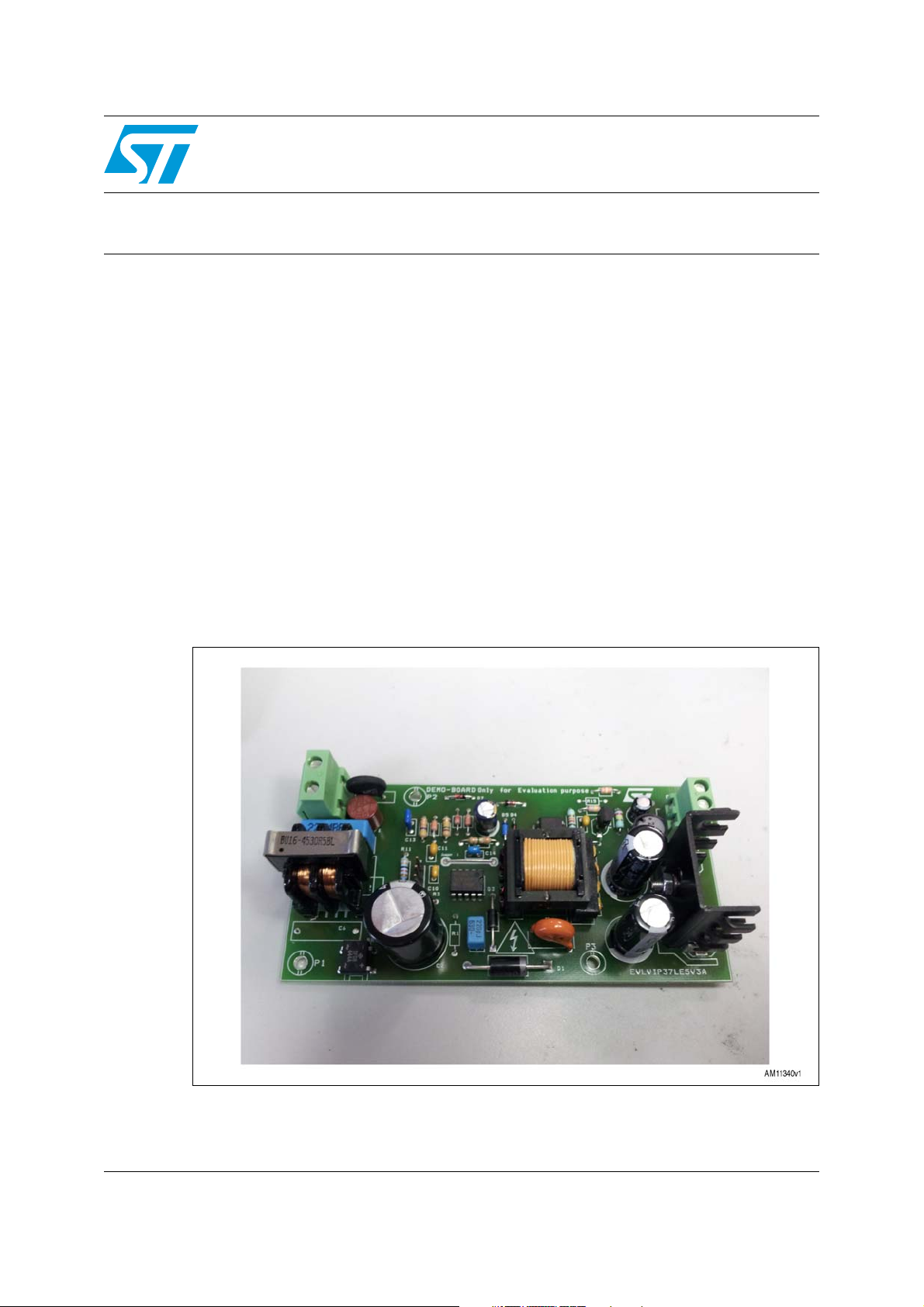
Figure 1. Demonstration board image: power supply board
May 2012 Doc ID 022455 Rev 1 1/33
www.st.com

Contents AN4007
Contents
1 Test board: design and evaluation . . . . . . . . . . . . . . . . . . . . . . . . . . . . . 4
1.1 Output voltage characteristics . . . . . . . . . . . . . . . . . . . . . . . . . . . . . . . . . . 7
1.2 Efficiency and light load measurements . . . . . . . . . . . . . . . . . . . . . . . . . . . 8
1.3 No-load consumption . . . . . . . . . . . . . . . . . . . . . . . . . . . . . . . . . . . . . . . . . 9
1.4 Light load consumption . . . . . . . . . . . . . . . . . . . . . . . . . . . . . . . . . . . . . . 10
1.5 Typical board waveforms . . . . . . . . . . . . . . . . . . . . . . . . . . . . . . . . . . . . . 11
1.6 Dynamic step load regulation . . . . . . . . . . . . . . . . . . . . . . . . . . . . . . . . . . 16
1.7 Soft-start . . . . . . . . . . . . . . . . . . . . . . . . . . . . . . . . . . . . . . . . . . . . . . . . . . 18
2 Protection features . . . . . . . . . . . . . . . . . . . . . . . . . . . . . . . . . . . . . . . . . 20
2.1 Overload and short-circuit protection . . . . . . . . . . . . . . . . . . . . . . . . . . . . 20
2.2 Overvoltage protection . . . . . . . . . . . . . . . . . . . . . . . . . . . . . . . . . . . . . . . 22
2.3 Secondary winding short-circuit and transformer saturation protection . . 23
2.4 Brownout protection . . . . . . . . . . . . . . . . . . . . . . . . . . . . . . . . . . . . . . . . . 25
3 Conducted noise measurements . . . . . . . . . . . . . . . . . . . . . . . . . . . . . . 27
4 Thermal measurements . . . . . . . . . . . . . . . . . . . . . . . . . . . . . . . . . . . . . 30
5 Conclusions . . . . . . . . . . . . . . . . . . . . . . . . . . . . . . . . . . . . . . . . . . . . . . . 31
6 Demonstration tools and documentation . . . . . . . . . . . . . . . . . . . . . . . 31
7 Revision history . . . . . . . . . . . . . . . . . . . . . . . . . . . . . . . . . . . . . . . . . . . 32
2/33 Doc ID 022455 Rev 1

AN4007 List of figures
List of figures
Figure 1. Demonstration board image: power supply board . . . . . . . . . . . . . . . . . . . . . . . . . . . . . . . . 1
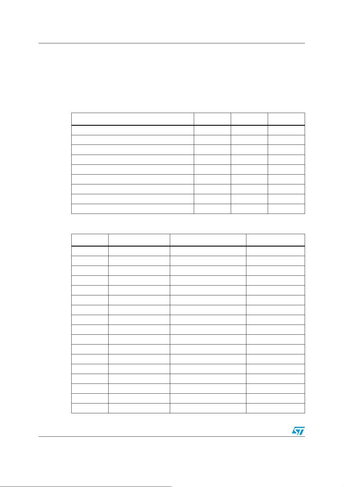
Figure 2. Electrical schematic . . . . . . . . . . . . . . . . . . . . . . . . . . . . . . . . . . . . . . . . . . . . . . . . . . . . . . . 6
Figure 3. Dimensional drawing . . . . . . . . . . . . . . . . . . . . . . . . . . . . . . . . . . . . . . . . . . . . . . . . . . . . . . 7
Figure 4. Line and load regulation . . . . . . . . . . . . . . . . . . . . . . . . . . . . . . . . . . . . . . . . . . . . . . . . . . . . 8
Figure 5. Efficiency vs. output power . . . . . . . . . . . . . . . . . . . . . . . . . . . . . . . . . . . . . . . . . . . . . . . . . . 9
Figure 6. No load consumption vs. input voltage . . . . . . . . . . . . . . . . . . . . . . . . . . . . . . . . . . . . . . . . 10
Figure 7. Light load consumption at different output power without brownout. . . . . . . . . . . . . . . . . . 10
Figure 8. Light load consumption at different output power with brownout . . . . . . . . . . . . . . . . . . . . 11
Figure 9. Drain current and voltage at full load 85 VAC. . . . . . . . . . . . . . . . . . . . . . . . . . . . . . . . . . . 12
Figure 10. Drain current and voltage at full load 115 VAC. . . . . . . . . . . . . . . . . . . . . . . . . . . . . . . . . . 12
Figure 11. Drain current and voltage at full load 230 VAC. . . . . . . . . . . . . . . . . . . . . . . . . . . . . . . . . . 13
Figure 12. Drain current and voltage at full load 264 VAC. . . . . . . . . . . . . . . . . . . . . . . . . . . . . . . . . . 13
Figure 13. Output voltage ripple at full load and 230 VAC. . . . . . . . . . . . . . . . . . . . . . . . . . . . . . . . . . 14
Figure 14. Output voltage ripple at full load and 115 VAC. . . . . . . . . . . . . . . . . . . . . . . . . . . . . . . . . . 15
Figure 15. Output voltage ripple during burst mode and 115 VAC . . . . . . . . . . . . . . . . . . . . . . . . . . . 15
Figure 16. Output voltage ripple during burst mode and 230 VAC . . . . . . . . . . . . . . . . . . . . . . . . . . . 16
Figure 17. Dynamic step load: 0 to 50% load . . . . . . . . . . . . . . . . . . . . . . . . . . . . . . . . . . . . . . . . . . . 17
Figure 18. Dynamic step load: 50 to 100% load . . . . . . . . . . . . . . . . . . . . . . . . . . . . . . . . . . . . . . . . . 17
Figure 19. Dynamic step load: 0 to 100% load . . . . . . . . . . . . . . . . . . . . . . . . . . . . . . . . . . . . . . . . . . 18
Figure 20. Soft-start feature . . . . . . . . . . . . . . . . . . . . . . . . . . . . . . . . . . . . . . . . . . . . . . . . . . . . . . . . . 19
Figure 21. Overload event: OLP triggering . . . . . . . . . . . . . . . . . . . . . . . . . . . . . . . . . . . . . . . . . . . . . 21
Figure 22. Overload event: continuous overload . . . . . . . . . . . . . . . . . . . . . . . . . . . . . . . . . . . . . . . . . 21
Figure 23. Overvoltage event: OVP triggering . . . . . . . . . . . . . . . . . . . . . . . . . . . . . . . . . . . . . . . . . . . 22
Figure 24. Overvoltage event: OVP triggering (magnification) . . . . . . . . . . . . . . . . . . . . . . . . . . . . . . 23
Figure 25. 2nd level OCP: protection tripping . . . . . . . . . . . . . . . . . . . . . . . . . . . . . . . . . . . . . . . . . . . 24
Figure 26. 2nd level OCP: steady-state operating conditions . . . . . . . . . . . . . . . . . . . . . . . . . . . . . . . 24
Figure 27. Brownout protection: converter’s power-down phase. . . . . . . . . . . . . . . . . . . . . . . . . . . . . 25
Figure 28. Brownout protection: converter’s wake-up . . . . . . . . . . . . . . . . . . . . . . . . . . . . . . . . . . . . . 26
Figure 29. Brownout protection: converter’s wake-up (magnification) . . . . . . . . . . . . . . . . . . . . . . . . . 26
Figure 30. CE average measurement at 115 VAC and full load: average measurement . . . . . . . . . . 27
Figure 31. CE average measurement at 230 VAC and full load: average measurement . . . . . . . . . . 28
Figure 32. CE average measurement at 115 VAC and full load: peak measurement . . . . . . . . . . . . . 28
Figure 33. CE average measurement at 230 VAC and full load: peak measurement . . . . . . . . . . . . . 29
Figure 34. Thermal map at 115 VAC and full load . . . . . . . . . . . . . . . . . . . . . . . . . . . . . . . . . . . . . . . . 30
Figure 35. Thermal map at 230 VAC and full load . . . . . . . . . . . . . . . . . . . . . . . . . . . . . . . . . . . . . . . . 30
Doc ID 022455 Rev 1 3/33
Test board: design and evaluation AN4007
1 Test board: design and evaluation
Ta bl e 1
bom list and
in
summarizes the electrical specifications of the power supply,
Figure 1
Ta bl e 3
and the PCB layout in
lists the transformer characteristics. The electrical schematic is shown
Figure 4
.
Ta bl e 2
provides the
Table 1. ALTAIR04-900 PLMS power supply: electrical specifications
Parameter Min. Typ. Max.
AC main input voltage 85 V
Mains frequency (fL) 50 Hz 60 Hz
Output voltage 4.75 V 5 V 5.25 V
Output current 3 A
Output ripple voltage 50 mV
Rated output power 15 W
Input power in standby 30 mW
Active mode efficiency 70%
Ambient operating temperature 60 °C
Table 2. VIPER37L demonstration board: bom list
Reference Part Description Note
AC
265 V
AC
R1 2.2 MΩ 1% tolerance
R2 3.9 MΩ 1% tolerance
R3 2 MΩ 1% tolerance
R4 150 kΩ 1% tolerance
R5 3.3 Ω
R6 330 Ω
R7 220 Ω
R8 12 kΩ
R9 120 kΩ 1% tolerance
R10 10 kΩ
R11 33 kΩ 1% tolerance
R12 39 kΩ 1% tolerance
R13 47 kΩ
R14 39 kΩ 1% tolerance
C1 220 pF - 630 V film capacitor
C2 33 µF - 400 V electrolytic
C3, C4 ZLK series 1200 µF - 16 V electrolytic Rubycon
4/33 Doc ID 022455 Rev 1

AN4007 Test board: design and evaluation
Table 2. VIPER37L demonstration board: bom list (continued)
Reference Part Description Note
C5 ZLH series 100 µF - 16 V electrolytic Rubycon
C6 B81133C1223M 22 nF - X2 EPCOS
C7 2.2 nF Y-CAP
C9, C10 10 nF ceramic – 25 V
C11 33 nF ceramic – 25 V
C12 22 µF - 35 V electrolytic
C13 2.2 nF ceramic – 25 V
C14 22 nF ceramic – 25 V
D1 1.5KE220A Transil™ ST
D2 STPS30L40CT Power Schottky diode ST
D3 STTH1L06A Ultra-fast high voltage diode ST
D5 BAT46RL Signal Schottky diode ST
D4, D7 1N4148 Signal diode NXP
D6 BZX79-C18 18 V Zener diode NXP
L1 ELC09D2R2F 2.2 H power inductor Panasonic
Note:
CM BU16-2530R7BL CM choke Coilcraft
BR DF08M-E3 Bridge diode Vishay
IC1 VIPER37LE Primary switching regulator ST
OPT KB817A Optoisolator Kingbright
TF 1715.0038 Flyback transformer Magnetica
Fs 1.6 A fuse Wickmann
NTC B57236S0160M NTC inrush current limiter EPCOS
If not otherwise specified, all resistors are ±5%, ¼ W
.
Doc ID 022455 Rev 1 5/33
Test board: design and evaluation AN4007
Figure 2. Electrical schematic
5V
L1
2.2uH
D2
STPS30L40CT
TF
C5
D1
1.5KE220
C1
220pF.
GND
100uF
R14
VR1
39k
TS431
C7
2.2nF
R9
120k
C4
1200uF
C3
1200uF
R6
330
R8
12k
OPTO3
KB817A
C9
10nF
R10
100k
GND
DRAIN
U1
D5
BAT46RL
D3
STTH1L06
D4
1N4148
R5
R2
3.9M
R4
150k
VIPER37LE
3.3
CONTROL
VDD
BR
CONT
FB
OPTO
KB817A
C13
2.2nF
C11
33nF
R13
47k
R12
39k
C2
BR
33uF
D7
1N4148
R1
2.2M
+
-
R3
2M
CM
2X25mH
3
C6
2
22nF – X2
4
1
C12
22uF
C14
22nF
6/33 Doc ID 022455 Rev 1
C10
10nF
R11
33k
JMP
R7
220
NTC
10
F1
1.5 A FUSE
D6
18V
AC IN AC IN
AM11341v1
AN4007 Test board: design and evaluation
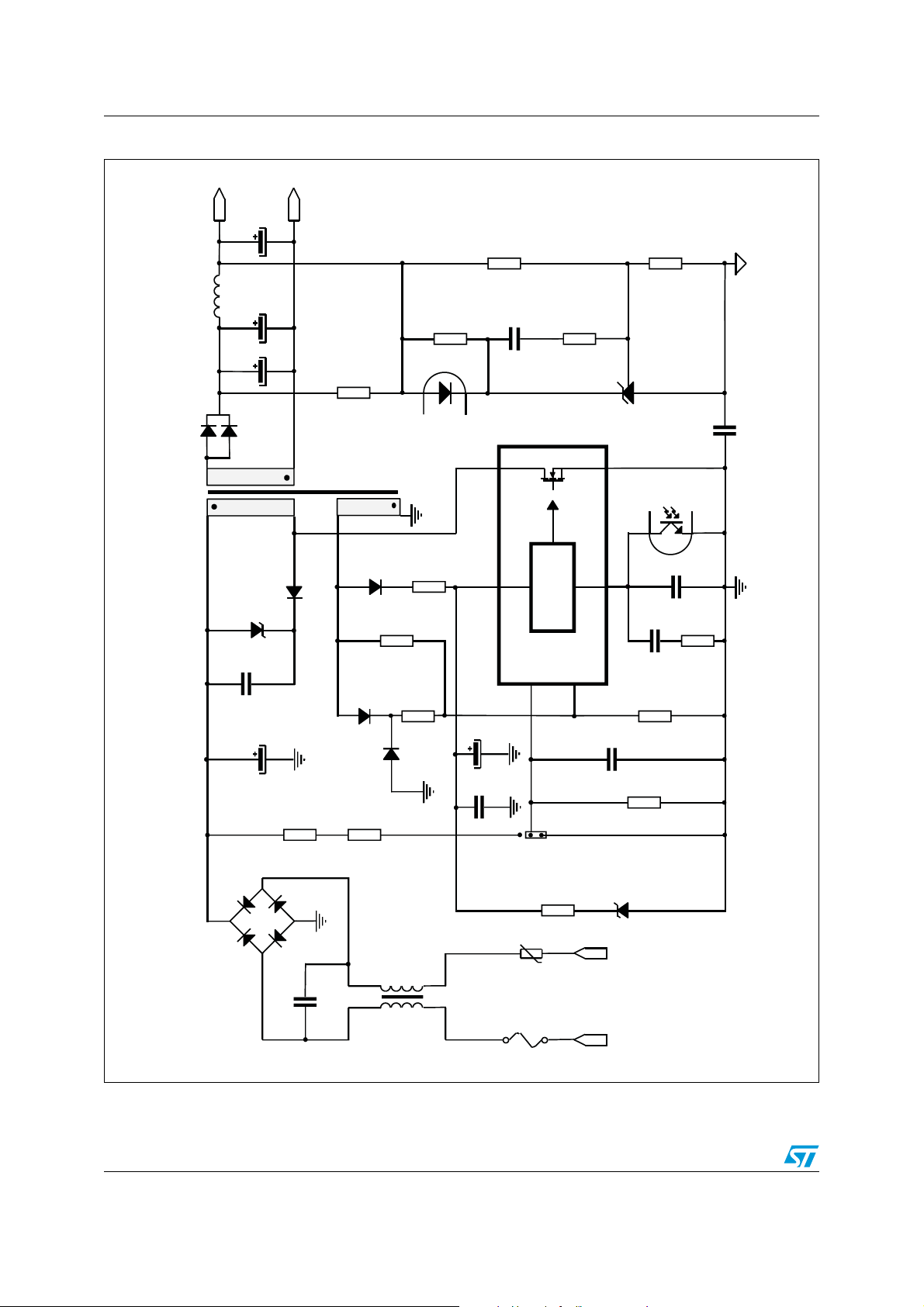
Table 3. VIPER37LE power supply: transformer characteristics
Manufacturer Magnetica Values
Part number 1715.0038
Primary inductance 1.3 mH
Leakage inductance 3% nom
Primary to secondary turn ratio 16.2 ± 5%
Primary to auxiliary turn ratio 5.90 ± 5%
Insulation primary-secondary AC 4 kV (1 s – 2 mA)
Figure 3. Dimensional drawing
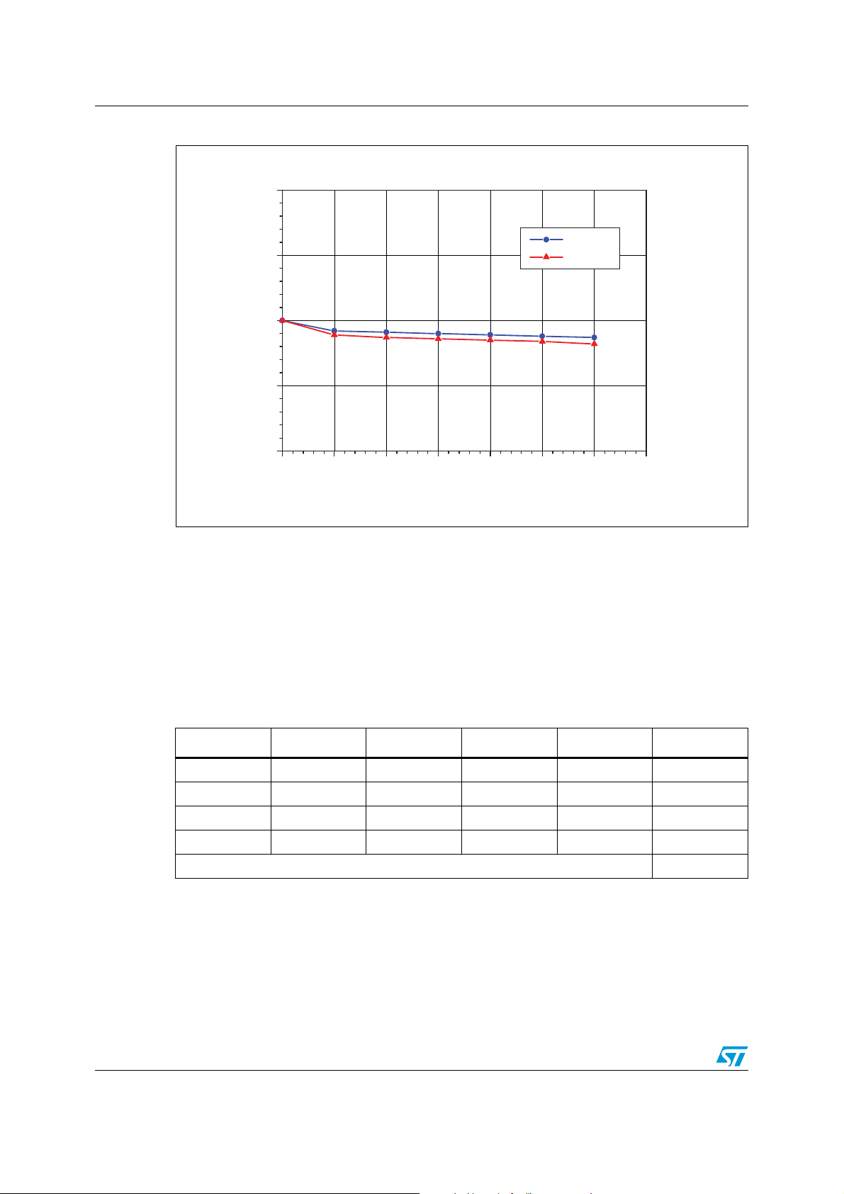
1.1 Output voltage characteristics
The output voltage of the board is measured in different line and load conditions.
shows the results: the output voltage variation range is a few tens of mV for all the tested
conditions.
All output voltages have been measured on the output connector of the board.
Doc ID 022455 Rev 1 7/33
Figure 4
Test board: design and evaluation AN4007
Figure 4. Line and load regulation
5.15
115Vac
5.10
5.05
Output voltage [V]
5.00
4.95
0.0 0.5 1.0 1.5 2.0 2.5 3.0 3.5
Output current [mA]
230Vac
AM11343v1
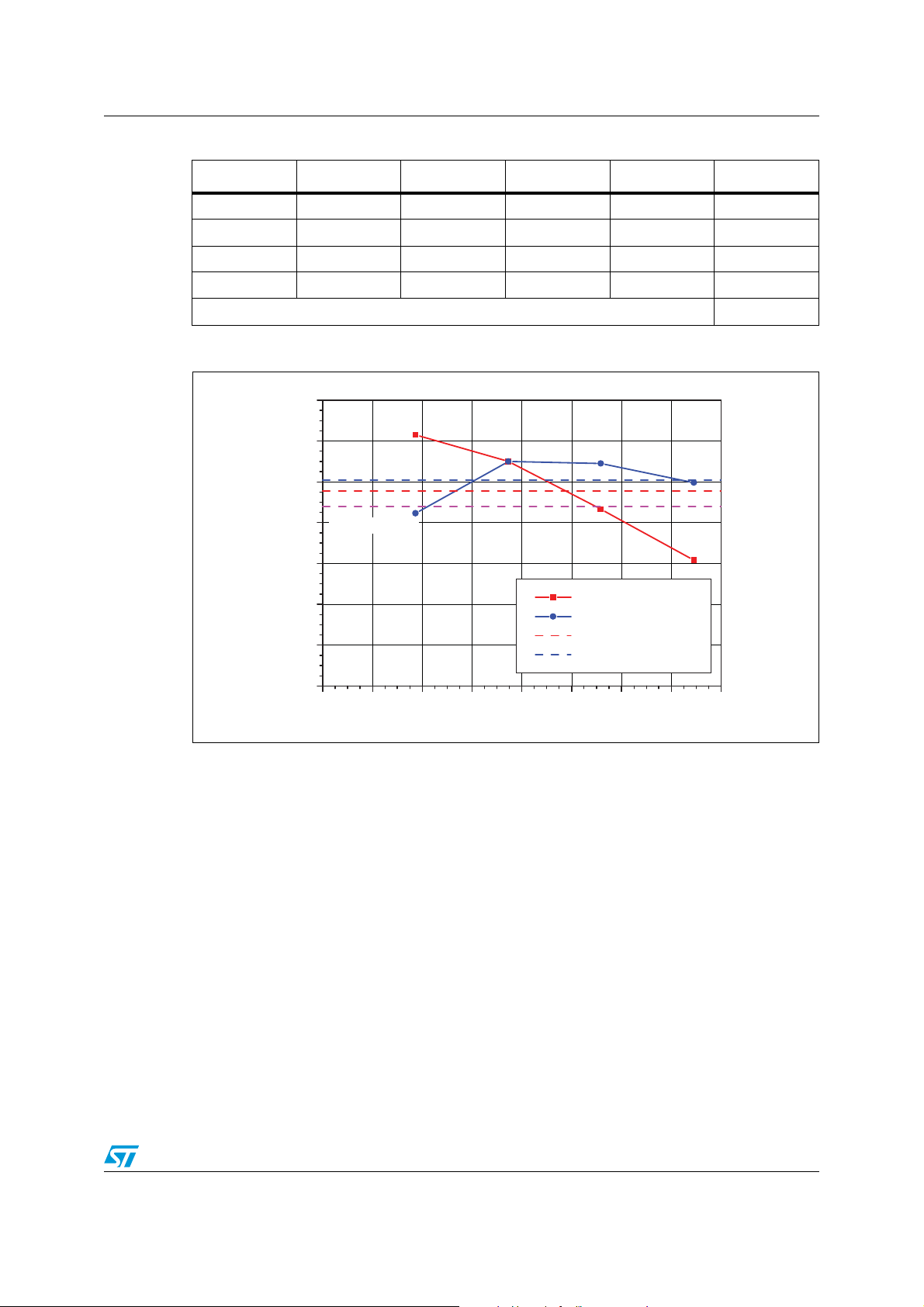
1.2 Efficiency and light load measurements
The efficiency of the converter has been measured in different load and line voltage
conditions.
In accordance with the ENERGY STAR
efficiency measurements have been performed at 25%, 50% and 75% and 100% of the
rated output power, at both 115 V
Table 4. Efficiency at 115 V
Load I
25%0.754.973.734.7678.31%
50% 1.5 4.97 7.46 9.65 77.25%
75% 2.25 4.97 11.17 14.75 75.74%
100% 3 4.97 14.91 19.86 75.08%
OUT
Average efficiency 76.59%
®
average active mode testing efficiency method, the
and 230 VAC.
AC
AC
V
OUT
Ta b le 4
P
OUT
and
Ta bl e 5
P
show the results:
IN
Efficiency
8/33 Doc ID 022455 Rev 1
AN4007 Test board: design and evaluation
Table 5. Efficiency at 230 V
Load I
25% 0.75 4.97 3.73 4.9 76.07%
50% 1.5 4.965 7.45 9.61 77.50%
75% 2.25 4.965 11.17 14.45 77.31%
100% 3 4.95 14.85 19.3 76.94%
OUT
AC
V
OUT
Average efficiency 76.96%
P
OUT
P
IN
Figure 5. Efficiency vs. output power
79
78
77
76
EPA 2.0 limit
75
Efficiency [%]
74
73
115Vac
230Vac
average @115Vac
averege @230Vac
Efficiency
72
02468 10 12 14 16
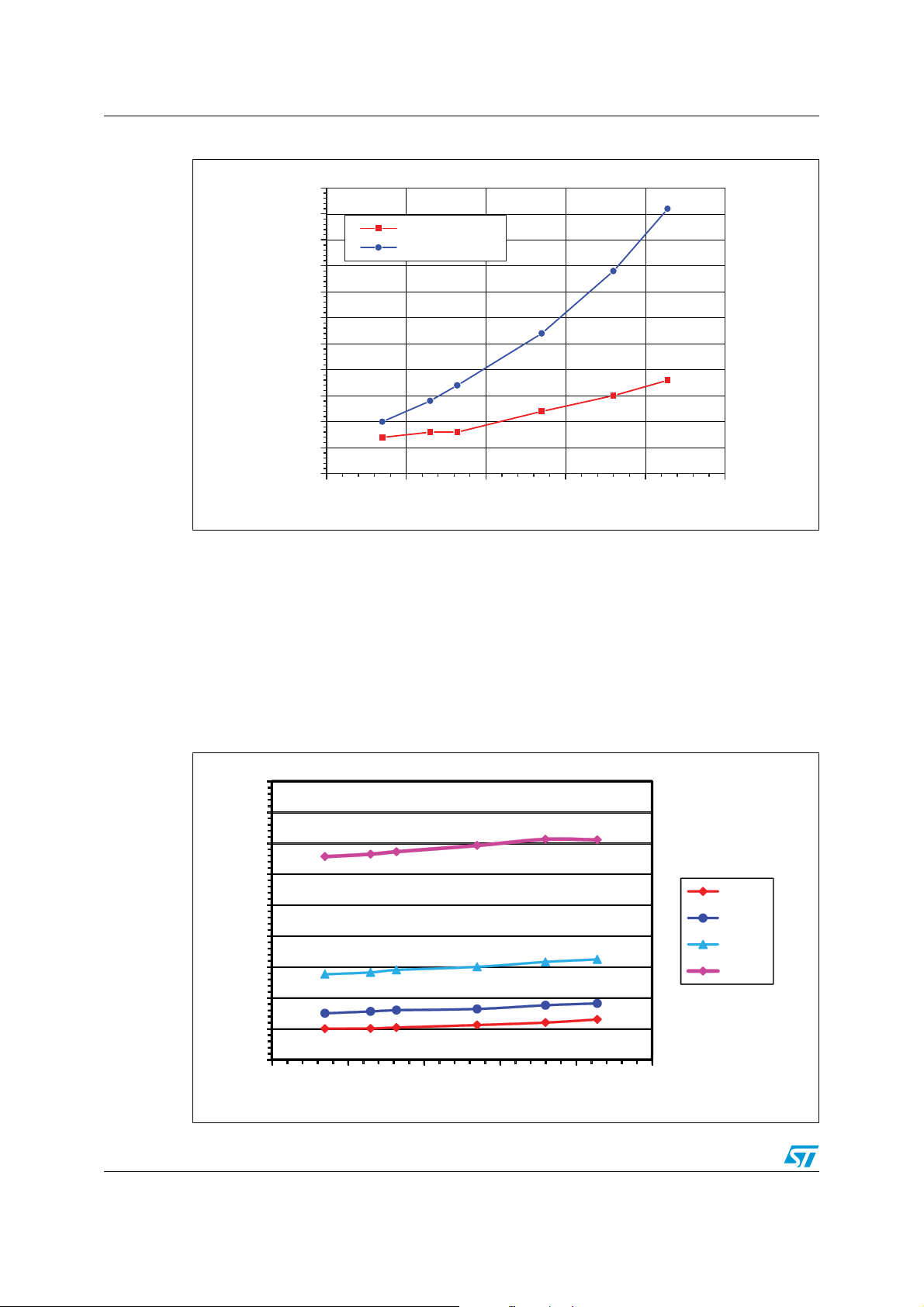
1.3 No-load consumption
The input power of the converter was measured in no load condition, with brownout
protection disabled (see relevant
enabled in the entire input voltage range.
The converter in the no load condition works always in burst mode so that the average
switching frequency is reduced. The presence of the brownout resistor divider (R16, R17
and R18, see schematic in
increases the input power consumption due to the power dissipated across it.
It is worth noting that often, if the converter is used as the standby power supply for LCD
TVs, PDPs or other applications, the EMI line filter often coincides with the main power
supply line filter that heavily contributes to standby consumption even if the power needed
by the auxiliary power supply is very low.
Figure 2
Output power [W]
Section 2.4: Brownout protection
) and brownout protection
) does not affect the average switching frequency but
AM11344v1
Doc ID 022455 Rev 1 9/33
Test board: design and evaluation AN4007
Figure 6. No load consumption vs. input voltage
65
60
55
50
45
40
35
30
Input power [mW]
25
20
15
10
50 100 150 200 250 300
No brownout
With brownout
Input voltage [Vac]
AM11347v1
1.4 Light load consumption
Even though the ENERGY STAR program does not have other requirements regarding light
load performance, except no load consumption, the user very often requires the input power
consumption when the output is loaded with a few tens of mW output power. Such
measurements were performed at different loads with brownout protection both enabled and
disabled, the results are reported below. The application meets the new EuP Lot 6
requirements.
Figure 7. Light load consumption at different output power without brownout
450
400
350
300
250
200
150
100
50
30mW
50mW
100mW
250mW
0
50 100 150 200 250 300
10/33 Doc ID 022455 Rev 1
AM11345v1

AN4007 Test board: design and evaluation
Figure 8. Light load consumption at different output power with brownout
450
400
350
300
250
30mW
50mW
200
150
100mW
250mW
100
50
0
50 100 150 200 250 300
AM11346v1
1.5 Typical board waveforms
Drain voltage and current waveforms were reported at nominal input voltages and for the
minimum and the maximum voltage of the converter input operating range.
show the drain current and the drain voltage waveforms at the two nominal input voltages
and full load, while
maximum input voltage range respectively.
The converter is designed to operate in continuous conduction mode (in full load condition)
at low line. CCM (continuous conduction mode) allows the reduction of the root mean
square currents value, at the primary side, in the power switch inside the VIPer and in the
primary winding of the transformer; at the secondary side in the output diode (D2) and in the
output capacitors (C3 and C4). Reducing RMS currents means reducing the power
dissipation in the VIPer™ and the stress of the secondary side components.
Figure 9
and 12 show the same waveforms at the minimum and
Figure 10
and 11
Doc ID 022455 Rev 1 11/33

Test board: design and evaluation AN4007
Figure 9. Drain current and voltage at full load 85 V
V
Ch1 (Max): 356.4
Ch2 (Max): 734.0 mA
AC
I
DS
V
DS
M: 4.0 µs/div
AM11348v1
Figure 10. Drain current and voltage at full load 115 V
Ch1 (Max): 417.6 V
Ch2 (Max): 792.0 mA
AC
I
DS
V
DS
M: 4.0 µs/div
AM11349v1
12/33 Doc ID 022455 Rev 1

AN4007 Test board: design and evaluation
Figure 11. Drain current and voltage at full load 230 V
Ch1 (Max): 578.0 V
Ch2 (Max): 750.0 mA
AC
I
DS
V
DS
M: 4.0 µs/div
AM11350v1
Figure 12. Drain current and voltage at full load 264 V
Ch1 (Max): 630.4 V
Ch2 (Max): 742.0 mA
AC
I
DS
V
DS
M: 4.0 µs/div
AM11351v1
Doc ID 022455 Rev 1 13/33

Test board: design and evaluation AN4007
The ripple at the switching frequency superimposed at the output voltage was also
measured. The board is provided with an LC filter to further reduce the ripple without
reducing the overall output capacitor’s ESR.
The voltage ripple across the output connector (V
were measured in order to verify the effectiveness of the LC filter:
output voltage ripple at full load when the converter input voltage is 115 V
) and before the LC filter (V
OUT
Figure 13
shows the
; while
AC
OUT_PRE
Figure 14
shows the output voltage ripple at full load when the converter input voltage is 230 V
Figure 13. Output voltage ripple at full load and 230 V
V
AC
OUT
V
OUT_PRE
AC
)
.
Ch1 (Pk-Pk): 18.73 mV
Ch2 (Pk-Pk): 298.3 mV
14/33 Doc ID 022455 Rev 1
M: 20.0 µs/div
AM11352v1

AN4007 Test board: design and evaluation
Figure 14. Output voltage ripple at full load and 115 V
V
V
Ch1 (Pk-Pk): 22.05 mV
Ch2 (Pk-Pk): 248.2 mV
AC
OUT
OUT_PRE
M: 20.0 µs/div
AM11353v1
Figure 15. Output voltage ripple during burst mode and 115 V
V
OUT
V
OUT_PRE
Ch1 (Pk-Pk): 19.79 mV
Ch2 (Pk-Pk): 56.45 mV
M: 400.0 µs/div
AC
AM11354v1
Doc ID 022455 Rev 1 15/33

Test board: design and evaluation AN4007
Figure 16. Output voltage ripple during burst mode and 230 V
V
OUT
V
OUT_PRE
Ch1 (Pk-Pk): 27.27 mV
Ch2 (Pk-Pk): 64.68 mV
M: 400.0 µs/div
AC
AM11355v1
1.6 Dynamic step load regulation
In any power supply it is important to measure the output voltage when the converter is
submitted to dynamic load variations, in order to be sure that good stability is ensured and
no overvoltage on undervoltage occurs.
The board under evaluation was submitted to dynamic load variations from 0 to 50% loads
(
Figure 17
In any tested condition, no abnormal oscillations were noticed on the output and the
over/undershoot were well within acceptable values.
), from 50% to 100% loads (
Figure 18
) and from 0 to 100% loads (
Figure 19
).
16/33 Doc ID 022455 Rev 1

AN4007 Test board: design and evaluation
Figure 17. Dynamic step load: 0 to 50% load
V
OUT
Ch1 (Max): 5.17 V
Ch1 (Min): 4.79 V
Ch2 (Max): 1.53 A
Figure 18. Dynamic step load: 50 to 100% load
V
I
OUT
OUT
M: 20.0 ms/div
AM11356v1
Ch1 (Max): 5.17 V
Ch1 (Min): 4.75 V
I
OUT
Ch2 (Max): 3.073 A
Ch2 (Min): 1.55 A
Doc ID 022455 Rev 1 17/33
M: 20.0 ms/div
AM11357v1

Test board: design and evaluation AN4007
Figure 19. Dynamic step load: 0 to 100% load
V
OUT
Ch1 (Max): 5.35 V
Ch1 (Min): 4.58 V
1.7 Soft-start
When the converter star ts, the output capacitor is discharged and needs some time to reach
the steady-state condition. During this time the power demand from the control loop is the
maximum while the reflected voltage is low. These two conditions could lead to a deep
continuous operating mode of the converter.
When the MOSFET is switched on, it cannot be switched off immediately as the minimum
on-time (T
converter, during this T
the converter as well as the device itself, the output diode, and the transformer. Transformer
saturation is also possible under these conditions.
ON_MIN
Ch2 (Max): 3.07 A
I
OUT
M: 20.0 µs/div
AM11358v1
) must elapse. Because of the deep continuous working mode of the
ON_MIN
, an excess of drain current can overstress the component of
To avoid all the described negative effects, the VIPER37LE implements an internal soft-start
feature. As the device starts to work, no matter what the control loop requests, the drain
current is allowed to increase from zero to the maximum value gradually.
The drain current limit is incremented in steps, and the values range from 0 to the fixed drain
current limitation value (values that can be adjusted through an external resistor) which is
divided into 16 steps. Each step length is 64 switching cycles. The total length of the softstart phase is about 8.5 ms.
Figure 20
shows the soft-start phase of the presented converter
when it is operating at minimum line voltage and maximum load.
18/33 Doc ID 022455 Rev 1

AN4007 Test board: design and evaluation
Figure 20. Soft-start feature
V
OUT
V
FB
Ch1 (Max): 5.18 V
I
DRAIN
M: 4.0 ms/div
AM11359v1
Doc ID 022455 Rev 1 19/33

Protection features AN4007
2 Protection features
The VIPER37LE has several protection features that considerably increase end-product
safety and reliability: overload protection, overvoltage protection, shorted secondary rectifier
detection and transformer saturation protection. In the following paragraphs all protections
are tested and the results are presented.
2.1 Overload and short-circuit protection
If the load power demand increases, the output voltage decreases and consequently the
feedback loop reacts, increasing the voltage on the FEEDBACK pin.
The FEEDBACK pin voltage increase leads to the PWM current set point increase, with the
rise of the power delivered to the output. This process ends when the delivered power
equals the load power requested.
If the load power demand exceeds the power capability (that can be adjusted using R
LIM
),
the voltage on the FEEDBACK pin continuously rises, but the drain current is limited to the
fixed current limitation value.
When the FEEDBACK pin voltage exceeds V
(3.3 V typ), the VIPER37LE takes it as a
FB_lin
warning status of an output overload condition. Before stopping the system, the device waits
for a time fixed by the FB capacitor. When the voltage on the FEEDBACK pin exceeds
V
, an internal pull-up circuit is disconnected and the pin starts sourcing a 3 A current
FB_lin
that charges the capacitor connected to the FEEDBACK pin itself. As the FEEDBACK pin's
voltage reaches the V
is not allowed to switch again until the V
threshold (4.8 V typ.), the power MOSFET stops switching and
FB_olp
voltage falls below V
DD
DD_RESTART
(4.5 V typ.).
If the short-circuit is not removed, the system starts to work in auto-restart mode: in this
case the MOSFET switches for a short period of time and the converter tries to deliver to the
output as much power as it can, and for a longer period where the device is not switching
and no power is processed.
As the duty cycle of power delivery is very low (around 4%), the average power throughput
is also very low, resulting in a very safe operation.
Figure 21
and 22 show the triggering of the overload and the operation with continuous
overload.
20/33 Doc ID 022455 Rev 1

AN4007 Protection features
Figure 21. Overload event: OLP triggering
V
FB
V
V
DRAIN
OUT
V1: 3.24 V
V2: 4.8 V
Figure 22. Overload event: continuous overload
V
DD
I
DRAIN
V
FB
M: 4.0 ms/div
AM11360v1
Duty cicle: 4.17 %
Doc ID 022455 Rev 1 21/33
M: 200.0 ms/div
AM11
361v1

Protection features AN4007
2.2 Overvoltage protection
An output overvoltage protection is implemented monitoring the voltage across the auxiliary
winding during the MOSFET turn-off time, through the diode D4 and the resistor dividers R4
and R12 connected on the CONT pin of the VIPER37LE. If this voltage exceeds the V
threshold (3 V typ.), an overvoltage event is assumed and the device is no longer allowed to
switch.
OVP
To re-enable operation, the V
voltage must be recycled. In order to provide high noise
DD
immunity and avoid that spikes erroneously trip the protection, a digital filter was
implemented so the CONT pin must sense a voltage higher than V
for four consecutive
OVP
cycles before stopping operation.
The protection can be tested by opening the resistor R9. In this way the converter operates
in open loop and the excess of power with respect to the load charges the output
capacitance, increasing the output voltage as the OVP is tripped and the converter stops
switching.
In
Figure 23
and 24 it is possible to see that output voltage increases and as it reaches the
value of 6.5 V the converter stops switching. In the same figure the CONT pin voltage is
reported. The crest value of the CONT pin voltage tracks the output voltage.
Figure 23. Overvoltage event: OVP triggering
V
CONT
Ch2 (Max): 6.48 V
22/33 Doc ID 022455 Rev 1
V
OUT
I
DRAIN
M: 400.0 µs/div
AM11362v1

AN4007 Protection features
Figure 24. Overvoltage event: OVP triggering (magnification)
V
CONT
V
OUT
I
DRAIN
Ch2 (Max): 3.08 V
M: 20.0 µs/div
AM11363v1
2.3 Secondary winding short-circuit and transformer saturation protection
The VIPER37LE is equipped with a hiccup mode overcurrent protection level.
If the drain current exceeds the second overcurrent threshold, the device enters a warning
state, at the next switching cycle, if the hiccup mode level is exceeded again, the device
assumes that a secondary winding short-circuit or a hard saturation of the transformer has
occurred, so the device stops operating and the MOSFET is no longer allowed to switch on.
In order to enable the MOSFET to switch on again, the V
to V
CCrestart
activation is not removed, the device again enters auto-restart mode. The extremely low
repetition rate ensures safe and reliable operation.
This protection was tested on the demonstration board. The secondary winding of the
transformer was shorted in different operating conditions.
behavior of the system during fault.
and then up to V
. If the cause of the hiccup mode overcurrent protection
CCon
voltage must be recycled down
CC
Figure 25
and 26 show the
Doc ID 022455 Rev 1 23/33

Protection features AN4007
Figure 25. 2nd level OCP: protection tripping
I
DRAIN
V
FB
Ch2 (Max): 2.14 A
Figure 26. 2
nd
level OCP: steady-state operating conditions
V
CC
I
DS
V
FB
M: 40.0 µs/div
AM11364v1
Ch2 (Freq.): 1.39 Hz
24/33 Doc ID 022455 Rev 1
Ch2 (Duty cycle): 1.71 %
M: 200.0 µs/div
AM11365v1

AN4007 Protection features
2.4 Brownout protection
Brownout protection is basically an unlatched device shutdown functionality whose typical
use is to sense mains undervoltage or unplugged mains. The VIPER37LE has a BR pin
dedicated to this function which must be connected to the DC HV bus through a voltage
divider.
If the protection is not required, it can be disabled by connecting the pin to ground. In the
presented converter, brownout protection is implemented but can be disabled by changing
the jumper JMP.
The converter's shutdown is accomplished by means of an internal comparator internally
referenced to 450 mV that disables the PWM if the voltage applied at the BR pin is below the
internal reference.
PWM operation is re-enabled as the BR pin voltage is more than 450 mV plus 50 mV of
voltage hysteresis that ensures noise immunity. The brownout comparator is also provided
with current hysteresis. An internal 10 A current generator is ON as long as the voltage
applied at the BROWNOUT pin is below 450 mV and is OFF if the voltage exceeds 450 mV
plus the voltage hysteresis.
In
Figure 27
bulk capacitor is discharged, the IC stops switching when the DC bus voltage falls below
78 V. This reduces the RMS input current and ensures monotonic output voltage decay.
the converter’s power-down is shown: once the main is disconnected and the
Figure 28
reaches 100 V, as the voltage on V
Figure 27. Brownout protection: converter’s power-down phase
and 29 show brownout protection during the wake-up phase: once the DC bus
pin is higher than V
DD
V
DD
V
BUS
V
BR
, the IC starts switching.
DDoff
V2: 459 mV
Doc ID 022455 Rev 1 25/33
V1: 78 V
M: 1.0 s/div
AM11366v1

Protection features AN4007
Figure 28. Brownout protection: converter’s wake-up
V
BUS
V
BR
V
DD
Ch2 (Freq.): 1.39 Hz
Figure 29. Brownout protection: converter’s wake-up (magnification)
V
BUS
V
BR
V
DD
Ch2 (duty cycle): 1.71 %
M: 100.0 ms/div
AM11367v1
V1: 457 mV
26/33 Doc ID 022455 Rev 1
M: 10.0 ms/div
AM11368v1

AN4007 Conducted noise measurements
3 Conducted noise measurements
A pre-compliance test for the EN55022 (Class B) European normative was also performed
on both average and peak measurements of the conducted noise emissions at full load and
nominal mains voltages.
test conditions there is a good margin for the measurements with respect to the limits, also
using the peak detector.
Figure 30
to 33 show the results. As seen in the diagrams, in all
Figure 30. CE average measurement at 115 V
and full load: average measurement
AC
Doc ID 022455 Rev 1 27/33

Conducted noise measurements AN4007
Figure 31. CE average measurement at 230 VAC and full load: average measurement
Figure 32. CE average measurement at 115 V
and full load: peak measurement
AC
28/33 Doc ID 022455 Rev 1

AN4007 Conducted noise measurements
Figure 33. CE average measurement at 230 VAC and full load: peak measurement
Doc ID 022455 Rev 1 29/33

Thermal measurements AN4007
4 Thermal measurements
A thermal analysis of the board was performed using an IR camera.
The board was submitted to full load at nominal input voltage and the thermal map was
taken 15 min. after the power-on at ambient temperature (25 °C).
Figure 34
Figure 34. Thermal map at 115 V
Figure 35. Thermal map at 230 V
and 35 show the results.
and full load
AC
and full load
AC
30/33 Doc ID 022455 Rev 1

AN4007 Conclusions
Table 6. Temperature of key components (T
=25 °C, emissivity=0.95 for all
amb
points)
Point Reference T [°C] at 115 V
A IC (VIPER37LE) 61.2 63.4
B D1 (Transil clamp) 82.8 81.6
C D2 (output diode) 44.1 45.0
D TF (flyback transformer) 67.3 70.0
E NTC (inrush limiter) 54.1 41.6
5 Conclusions
A 15 W wide range single-output flyback converter using the new VIPER37LE has been
introduced and the results given.
The presented flyback converter is suitable as an external adapter or as an auxiliary power
supply in consumer equipment. Special attention was paid to low load performance and the
bench results are good with very low input power in light load condition.
The efficiency performances were compared with the requirements of the ENERGY STAR
program (version 2.0) for external AC/DC adapters with very good results, the measured
Active mode efficiency is always higher with respect to the minimum required.
AC
T [°C] at 230 V
AC
6 Demonstration tools and documentation
The VIPER37LE demonstration board order code is: EVLVIP37LE5V3A.
Further information about this product is available in the VIPER37 datasheet at www.st.com
.
Doc ID 022455 Rev 1 31/33

Revision history AN4007
7 Revision history
Table 7. Document revision history
Date Revision Changes
16-May-2012 1 Initial release.
32/33 Doc ID 022455 Rev 1

AN4007
Please Read Carefully:
Information in this document is provided solely in connection with ST products. STMicroelectronics NV and its subsidiaries (“ST”) reserve the
right to make changes, corrections, modifications or improvements, to this document, and the products and services described herein at any
time, without notice.
All ST products are sold pursuant to ST’s terms and conditions of sale.
Purchasers are solely responsible for the choice, selection and use of the ST products and services described herein, and ST assumes no
liability whatsoever relating to the choice, selection or use of the ST products and services described herein.
No license, express or implied, by estoppel or otherwise, to any intellectual property rights is granted under this document. If any part of this
document refers to any third party products or services it shall not be deemed a license grant by ST for the use of such third party products
or services, or any intellectual property contained therein or considered as a warranty covering the use in any manner whatsoever of such
third party products or services or any intellectual property contained therein.
UNLESS OTHERWISE SET FORTH IN ST’S TERMS AND CONDITIONS OF SALE ST DISCLAIMS ANY EXPRESS OR IMPLIED
WARRANTY WITH RESPECT TO THE USE AND/OR SALE OF ST PRODUCTS INCLUDING WITHOUT LIMITATION IMPLIED
WARRANTIES OF MERCHANTABILITY, FITNESS FOR A PARTICULAR PURPOSE (AND THEIR EQUIVALENTS UNDER THE LAWS
OF ANY JURISDICTION), OR INFRINGEMENT OF ANY PATENT, COPYRIGHT OR OTHER INTELLECTUAL PROPERTY RIGHT.
UNLESS EXPRESSLY APPROVED IN WRITING BY TWO AUTHORIZED ST REPRESENTATIVES, ST PRODUCTS ARE NOT
RECOMMENDED, AUTHORIZED OR WARRANTED FOR USE IN MILITARY, AIR CRAFT, SPACE, LIFE SAVING, OR LIFE SUSTAINING
APPLICATIONS, NOR IN PRODUCTS OR SYSTEMS WHERE FAILURE OR MALFUNCTION MAY RESULT IN PERSONAL INJURY,
DEATH, OR SEVERE PROPERTY OR ENVIRONMENTAL DAMAGE. ST PRODUCTS WHICH ARE NOT SPECIFIED AS "AUTOMOTIVE
GRADE" MAY ONLY BE USED IN AUTOMOTIVE APPLICATIONS AT USER’S OWN RISK.
Resale of ST products with provisions different from the statements and/or technical features set forth in this document shall immediately void
any warranty granted by ST for the ST product or service described herein and shall not create or extend in any manner whatsoever, any
liability of ST.
ST and the ST logo are trademarks or registered trademarks of ST in various countries.
Information in this document supersedes and replaces all information previously supplied.
The ST logo is a registered trademark of STMicroelectronics. All other names are the property of their respective owners.
© 2012 STMicroelectronics - All rights reserved
STMicroelectronics group of companies
Australia - Belgium - Brazil - Canada - China - Czech Republic - Finland - France - Germany - Hong Kong - India - Israel - Italy - Japan -
Malaysia - Malta - Morocco - Philippines - Singapore - Spain - Sweden - Switzerland - United Kingdom - United States of America
www.st.com
Doc ID 022455 Rev 1 33/33
 Loading...