

Page 1

AN3995
Application note
Getting started tutorial
for SPC564Bxx and SPC56ECxx family
Introduction
The SPC564Bxx and SPC56ECxx is a family of Power Architecture® based microcontrollers
that target automotive vehicle body and gateway applications such as Central body
controller, Smart junction boxes, Front modules, High end gateway, Combined Body
controller and gateway.
These dual core architecture devices contain an e200z4d and e200z0h core, compliant with
the Power Architecture standard.
It provides the scalability needed to implement platform approaches and delivers the
performance required by increasingly sophisticated software architectures.
These devices feature up to 3 MB of internal Flash and up to 256 KB of internal SRAM
memory.
It operates at speeds of up to 120 MHz and offers high performance processing optimized
for low power consumption.
The SPC564Bxx and SPC56ECxx family expands the range of the SPC560B/C
microcontroller family but differs from it by being the first device to feature the e200z4d core
and the e200z0h in a dual core configuration.
The differences between this family and the previous one (SPC560B/C) mean that the
initialization and configuration are different.
This application note details the steps required to properly initialize the SPC564Bxx and
SPC56ECxx from reset as well as how to control the second core. An example code is
described throughout the application note to explain the steps.
It is intended that this application note is read along with the SPC564Bxx and SPC56ECxx
Reference Manual, RM0070 that can be obtained from the STMicroelectronics
http://www.st.com (see Section C.1: Reference document).
®
website at
November 2011 Doc ID 022384 Rev 1 1/49
www.st.com
Page 2

Contents AN3995
Contents
1 Application example description . . . . . . . . . . . . . . . . . . . . . . . . . . . . . . . 6
2 Microcontroller boot . . . . . . . . . . . . . . . . . . . . . . . . . . . . . . . . . . . . . . . . . 7
2.1 Boot mechanism . . . . . . . . . . . . . . . . . . . . . . . . . . . . . . . . . . . . . . . . . . . . . 7
2.1.1 Bootable sectors and RCHW . . . . . . . . . . . . . . . . . . . . . . . . . . . . . . . . . . 8
3 e200z4d initialization and example code . . . . . . . . . . . . . . . . . . . . . . . 10
3.1 Creating e200z4d Flash boot file . . . . . . . . . . . . . . . . . . . . . . . . . . . . . . . 10
3.1.1 MMU remarks . . . . . . . . . . . . . . . . . . . . . . . . . . . . . . . . . . . . . . . . . . . . 10
3.1.2 Configure MMU for SRAM . . . . . . . . . . . . . . . . . . . . . . . . . . . . . . . . . . . 13
3.1.3 Initialize the SRAM ECC . . . . . . . . . . . . . . . . . . . . . . . . . . . . . . . . . . . . 14
3.1.4 Configure MMU for Flash . . . . . . . . . . . . . . . . . . . . . . . . . . . . . . . . . . . . 14
3.1.5 Configure MMU for Peripheral Bridge . . . . . . . . . . . . . . . . . . . . . . . . . . 16
3.1.6 Memory initialization . . . . . . . . . . . . . . . . . . . . . . . . . . . . . . . . . . . . . . . 16
3.1.7 Performance Hints Initialization . . . . . . . . . . . . . . . . . . . . . . . . . . . . . . . 19
3.2 e200z4d device configuration from C code . . . . . . . . . . . . . . . . . . . . . . . 24
3.2.1 Disable watchdog . . . . . . . . . . . . . . . . . . . . . . . . . . . . . . . . . . . . . . . . . . 24
3.2.2 Mode configuration and clocking . . . . . . . . . . . . . . . . . . . . . . . . . . . . . . 25
3.2.3 Clock & PLL configuration . . . . . . . . . . . . . . . . . . . . . . . . . . . . . . . . . . . 28
3.2.4 Configure Cache . . . . . . . . . . . . . . . . . . . . . . . . . . . . . . . . . . . . . . . . . . 29
3.2.5 Starting the e200z0h core . . . . . . . . . . . . . . . . . . . . . . . . . . . . . . . . . . . 30
3.3 The e200z4d example code . . . . . . . . . . . . . . . . . . . . . . . . . . . . . . . . . . . 31
4 e200z0h Initializations and example code . . . . . . . . . . . . . . . . . . . . . . 32
4.1 e200z0h startup code . . . . . . . . . . . . . . . . . . . . . . . . . . . . . . . . . . . . . . . . 32
Appendix A Application code example . . . . . . . . . . . . . . . . . . . . . . . . . . . . . . . . 34
A.1 main.c file . . . . . . . . . . . . . . . . . . . . . . . . . . . . . . . . . . . . . . . . . . . . . . . . . 34
A.2 crt0_corez4_Flash.s . . . . . . . . . . . . . . . . . . . . . . . . . . . . . . . . . . . . . . . . . 38
Appendix B Linker file . . . . . . . . . . . . . . . . . . . . . . . . . . . . . . . . . . . . . . . . . . . . . . 44
Appendix C Further information . . . . . . . . . . . . . . . . . . . . . . . . . . . . . . . . . . . . . . 47
C.1 Reference document . . . . . . . . . . . . . . . . . . . . . . . . . . . . . . . . . . . . . . . . . 47
2/49 Doc ID 022384 Rev 1
Page 3

AN3995 Contents
C.2 Acronyms and abbreviations . . . . . . . . . . . . . . . . . . . . . . . . . . . . . . . . . . . 47
Revision history . . . . . . . . . . . . . . . . . . . . . . . . . . . . . . . . . . . . . . . . . . . . . . . . . . . . 48
Doc ID 022384 Rev 1 3/49
Page 4

List of tables AN3995
List of tables
Table 1. Boot mode selection . . . . . . . . . . . . . . . . . . . . . . . . . . . . . . . . . . . . . . . . . . . . . . . . . . . . . . . 7
Table 2. RCHW field description. . . . . . . . . . . . . . . . . . . . . . . . . . . . . . . . . . . . . . . . . . . . . . . . . . . . . 9
Table 3. Example of MMU configuration. . . . . . . . . . . . . . . . . . . . . . . . . . . . . . . . . . . . . . . . . . . . . . 12
Table 4. Memory partition schema . . . . . . . . . . . . . . . . . . . . . . . . . . . . . . . . . . . . . . . . . . . . . . . . . . 44
Table 5. Acronyms and abbreviations . . . . . . . . . . . . . . . . . . . . . . . . . . . . . . . . . . . . . . . . . . . . . . . 47
Table 6. Document revision history . . . . . . . . . . . . . . . . . . . . . . . . . . . . . . . . . . . . . . . . . . . . . . . . . 48
4/49 Doc ID 022384 Rev 1
Page 5

AN3995 List of figures
List of figures
Figure 1. Boot sector structure. . . . . . . . . . . . . . . . . . . . . . . . . . . . . . . . . . . . . . . . . . . . . . . . . . . . . . . 9
Figure 2. SPC564Bxx/SPC56ECxx block diagram . . . . . . . . . . . . . . . . . . . . . . . . . . . . . . . . . . . . . . 11
Figure 3. MMU configuration code for SRAM . . . . . . . . . . . . . . . . . . . . . . . . . . . . . . . . . . . . . . . . . . 13
Figure 4. SRAM ECC initialization code . . . . . . . . . . . . . . . . . . . . . . . . . . . . . . . . . . . . . . . . . . . . . . 14
Figure 5. MMU configuration code for Flash . . . . . . . . . . . . . . . . . . . . . . . . . . . . . . . . . . . . . . . . . . . 15
Figure 6. Code to copy configuration code from Flash to SRAM . . . . . . . . . . . . . . . . . . . . . . . . . . . . 15
Figure 7. MMU configuration code for peripherals area. . . . . . . . . . . . . . . . . . . . . . . . . . . . . . . . . . . 16
Figure 8. Booting flow using GHS startup libraries . . . . . . . . . . . . . . . . . . . . . . . . . . . . . . . . . . . . . . 17
Figure 9. Startup file: __ghs_board_memory_init . . . . . . . . . . . . . . . . . . . . . . . . . . . . . . . . . . . . . . . 18
Figure 10. Startup file: branch to GHS startup libraries . . . . . . . . . . . . . . . . . . . . . . . . . . . . . . . . . . . . 18
Figure 11. Startup file: enable BTB and SPE. . . . . . . . . . . . . . . . . . . . . . . . . . . . . . . . . . . . . . . . . . . . 19
Figure 12. Startup file: Flash Configuration code. . . . . . . . . . . . . . . . . . . . . . . . . . . . . . . . . . . . . . . . . 20
Figure 13. Startup file: SRAM wait states configuration code . . . . . . . . . . . . . . . . . . . . . . . . . . . . . . . 20
Figure 14. Startup file: XBAR register configuration values . . . . . . . . . . . . . . . . . . . . . . . . . . . . . . . . . 21
Figure 15. Startup file: XBAR configuration code . . . . . . . . . . . . . . . . . . . . . . . . . . . . . . . . . . . . . . . . 22
Figure 16. Cache Configuration Code . . . . . . . . . . . . . . . . . . . . . . . . . . . . . . . . . . . . . . . . . . . . . . . . . 23
Figure 17. Environment configurations code . . . . . . . . . . . . . . . . . . . . . . . . . . . . . . . . . . . . . . . . . . . . 24
Figure 18. SWT disabling code . . . . . . . . . . . . . . . . . . . . . . . . . . . . . . . . . . . . . . . . . . . . . . . . . . . . . . 25
Figure 19. Mode entry diagram . . . . . . . . . . . . . . . . . . . . . . . . . . . . . . . . . . . . . . . . . . . . . . . . . . . . . . 26
Figure 20. Mode Initialization Code . . . . . . . . . . . . . . . . . . . . . . . . . . . . . . . . . . . . . . . . . . . . . . . . . . . 26
Figure 21. Peripheral Control Registers. . . . . . . . . . . . . . . . . . . . . . . . . . . . . . . . . . . . . . . . . . . . . . . . 27
Figure 22. Run peripheral control registers . . . . . . . . . . . . . . . . . . . . . . . . . . . . . . . . . . . . . . . . . . . . . 27
Figure 23. System clock dividers configuration code . . . . . . . . . . . . . . . . . . . . . . . . . . . . . . . . . . . . . . 28
Figure 24. PLL configuration code . . . . . . . . . . . . . . . . . . . . . . . . . . . . . . . . . . . . . . . . . . . . . . . . . . . . 29
Figure 25. Application code: the main function . . . . . . . . . . . . . . . . . . . . . . . . . . . . . . . . . . . . . . . . . . 31
Figure 26. e200z0h startup code . . . . . . . . . . . . . . . . . . . . . . . . . . . . . . . . . . . . . . . . . . . . . . . . . . . . . 33
Doc ID 022384 Rev 1 5/49
Page 6

Application example description AN3995
1 Application example description
This application note describes the necessary steps to configure the device in order to run
two independent codes on the two cores.
This family is quite different from the previous one, indeed apart from the memories size
now it has been introduced the dual core concept: in the SPC564Bxx and SPC56ECxx
family the primary core is an e200z4d while the second one is a e200z0h.
While the second core (e200z0h) is thought only as performance core (only to speed up the
execution), the introduction of the e200z4d implies that the user has a more powerful
architecture to cope with the application tasks.
The availability of MMU, ICache and Signal Processing instructions enhance the
performance, but require the correct configuration.
The example code described herein toggles two LEDs with each core running the
application independent of the other.
It has been chosen to treat the two applications separately to better understand the dual
core concept even for compiler projects: of course each project produces one executable
image. The user then has to program the device with both executable images (the
instruction codes are located in different places).
Following this strategy the device is perceived as two separate MCUs each with proprietary
Flash and SRAM.
In this application note, it has been decided to split (in equal parts) the Flash and the SRAM
for both cores.
The memory partition and the XBAR (crossbar architecture) have been optimized for dual
core operations and in particular to give priority to e200z4d core (see Section 3.1.7:
Performance Hints Initialization):
● The SRAM is split over 2 slave ports, 0x4000_0000 to 0x4001_FFFF on slave port 2
(used by e200z4d) and 0x4002_0000 to 0x4003_FFFF on slave port 3 (used by
e200z0h);
● There are 2 Flash ports, z4 instruction port on slave port 0 and a second Flash port for
everything else on slave port 1.
By splitting the SRAM in the linker file(s) so that the e200z4d has access to one block and
the e200z0h has access to the other block, crossbar contentions are generally avoided
between the cores for SRAM access
(a)
(see Appendix B: Linker file).
a. When, for example, there are large amounts of DMA transfers to/from SRAM it could be useful to use the
SRAM allocated to the processor which allows fewer accesses to SRAM. User has to take care that none of
this prevents either core from writing the full SRAM array so care has to be taken in software (using
semaphores and / or software interrupts) to ensure memory coherency.
6/49 Doc ID 022384 Rev 1
Page 7
AN3995 Microcontroller boot
2 Microcontroller boot
This chapter describes the configuration required by the user, and the steps performed by
the microcontroller
(b)
and in particular, by the SSCM (System Status and Configuration
Module), in order to achieve a successful boot from Flash memory.
For further information, look at SPC564Bxx and SPC56ECxx Reference Manual (see
Section C.1: Reference document).
2.1 Boot mechanism
SPC564Bxx and SPC56ECxx family (as other SPC56xx devices), has two hardware boot
configuration pins, FAB (Force Alternate Boot mode) and ABS (Alternate Boot Select).
These 2 external pins on the microcontroller are latched during reset and used by the SSCM
to determine whether the microcontroller boots from Flash memory or attempts a serial
download via FlexCAN or LINFlex (RS232) (see Tab l e 1 ).
In this application note, the focus is on the default operating mode: the Flash boot mode.
Table 1. Boot mode selection
Mode FAB pin (PA[9]) ABS pin (PA[8])
Flash Boot (Default Mode) 0 –
Serial Boot (LINFlex) 1 0
Serial Boot (FlexCAN) 1 1
When the device is powered on, the SSCM (System Status Configuration Module) searches
the pre-determined locations in Flash for a valid RCHW (Reset Configuration Half Word)
(see Section 2.1.1: Bootable sectors and RCHW).
● If a valid BOOT_ID is found, the SSCM reads the VLE bit and the boot vector address
(as well as the CSE block size).
● If a valid BOOT_ID is not found, the SSCM starts the process of putting the
microcontroller (e200z4d) into static mode
(c)
. See SPC564Bxx and SPC56ECxx family
Reference Manual for detailed information (see Section C.1: Reference document).
Note: The static mode differs from safe mode. Static mode is a non-operational mode which can
only be entered via the BAM (Boot Assist Module).
b. The booting mechanism has an impact only on the e200z4d core.
c. Static Mode Sequence:
1. The SSCM creates a 4 KB MMU page at the start of the BAM with the VLE bit set (the BAM is VLE code).
2. The SSCM then sets the CPU core (e200z4d) instruction pointer to the BAM address and the core starts to
execute the code to enter static mode as follows:
- the Software Watchdog Timer (SWT) is enabled;
- the core executes the "wait" instruction which halts the core.
After the microcontroller enters static mode, the SWT periodically resets the core (approximately every 10 ms)
to re-attempt a boot from Flash memory.
Doc ID 022384 Rev 1 7/49
Page 8

Microcontroller boot AN3995
In all these conditions, the e200z0h core remains held in reset: for further information please
refer to SPC564Bxx and SPC56ECxx Reference Manual, RM0070 (see Section C.1:
Reference document).
In order to access memory (for the e200z4d core), a valid MMU TLB entry has to be
created. The SSCM does this automatically by reading the reset vector and modifying TLB
entry 0 to create a 4 KB page containing the reset vector address.
The MMU VLE bit is set depending on the status of the VLE bit within the RCHW. The 4 KB
MMU page
(d)
must be 4 KB aligned. This means that the most efficient place to put the
application code is immediately after the boot sector (see Section 2.1.1: Bootable sectors
and RCHW). So in order to maximize the available space inside the 4 KB block, the reset
vector should be set close to the start of a 4 KB boundary.
Note: For example, if the reset vector is set to address 0x0000_0020, then the SSCM aligns the 4
KB MMU page to the start of the 4 KB aligned block containing address 0x0000_0020 – an
MMU page starting at address 0x0000_0000.
Similarly, if the reset vector is set to address 0x0000_0FF0 which is towards the end of an
aligned 4 KB block, the MMU page still has to start at 0x0000_0000 leaving very little room
in the 4 KB MMU page for code execution.
Finally, the SSCM sets the e200z4d core instruction pointer to the reset vector address and
starts the core running.
2.1.1 Bootable sectors and RCHW
In order to successfully boot from Flash memory, the user must program two 32-bit fields
into one of the 5 possible boot blocks (see Figure 1).
The entities to program are:
● 16-bit Reset Configuration Half Word (RCHW), which contains:
– A BOOT_ID field that must be correctly set to 0x5A in order to "validate" the boot
sector;
– A VLE bit which configures the initial MMU entry to either Power Architecture Book
VLE or Power Architecture Book III-E as described later on in this chapter;
● 32-bit reset vector (this is the start address of the user code)
The boot sector also contains a 32-bit field containing the size of the block of data to be
checked by the CSE (Cryptographic Security Engine) during a secure boot. See
SPC564Bxx and SPC56ECxx family Reference Manual, RM0070 for detailed information
(Section C.1: Reference document).
Note: Application code can then be programmed from offset address 0x000C.
d. The 4 KB block provides sufficient space to the user to:
1. Add MMU entries for SRAM and peripherals
2. Perform standard system initialization tasks (initialize the SRAM, setup stack, copy constant data)
3. Transfer execution to RAM, re-define the Flash memory MMU entry and transfer execution back to Flash
memory.
8/49 Doc ID 022384 Rev 1
Page 9
AN3995 Microcontroller boot
Figure 1. Boot sector structure
0x0000_0000
0x0000_8000
0x0000_C000
0x0001_0000
0x0001_8000
Boot sector 0
32 KB
Boot sector 1
16 KB
Boot sector 2
16 KB
Boot sector 3
32 KB
Boot sector 4
32 KB
Bit 0 Bit 31
0x0
(RCHW)
0x4
0x8
0xC
Code Flash memory
The structure of RCHW is described in Ta bl e 2 :
Table 2. RCHW field description
Boot sector structure
678 1516
Reserved Reserved
32-bit reset vector (points to star t address of application code)
BOOT_ID
(0x5A)
VLE
Size of Flash memory array to be verified by CSE
(see the CSE chapter)
Application code (from offset 0xC and onward)
Field Description
VLE Bit
VLE
0 MMU TLB Entry 0 is configured for Power Architecture Book III-E.
1 MMU TLB Entry 0 is configured for Power Architecture Book VLE.
BOOT_ID
Boot identifier.
If BOOT_ID = 0x5A, the boot sector is considered valid and bootable.
Doc ID 022384 Rev 1 9/49
Page 10

e200z4d initialization and example code AN3995
3 e200z4d initialization and example code
3.1 Creating e200z4d Flash boot file
In order to run an application from Flash memory, the user code must perform a series of
mandatory actions for proper execution:
● Provide reset vector in the location after the RCHW (Section 2.1: Boot mechanism);
● Configure MMU;
● Initialize SRAM (ECC) (see Section 3.1.3: Initialize the SRAM ECC);
● Configure wait states for Flash and SRAM (see Section 3.1.7: Performance Hints
Initialization);
● Configure XBAR (see Section 3.1.7: Performance Hints Initialization);
● Enable SPE (Signal Processing Extension) instructions if needed by the application
● Enable BTB
Initialization).
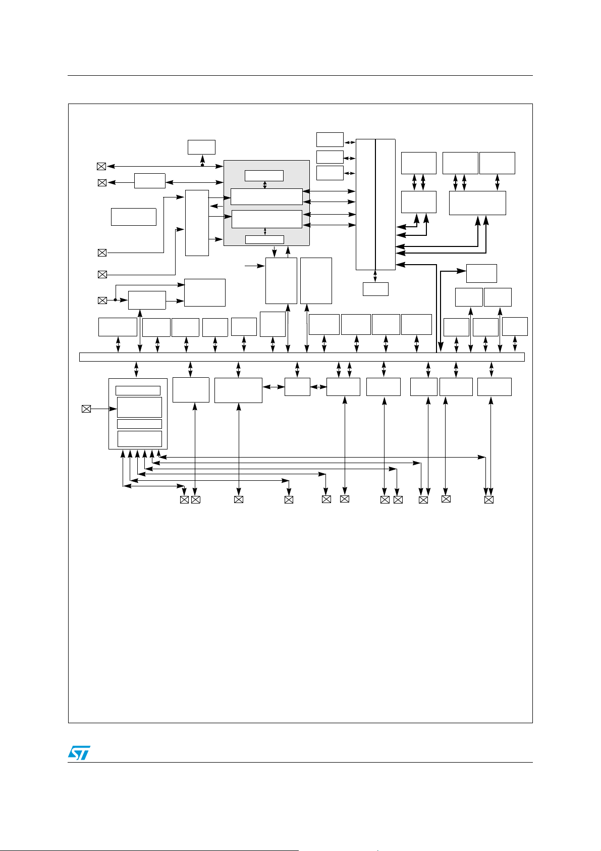
3.1.1 MMU remarks
The e200z4d core has a Memory Management Unit (MMU)
the e200z4d core to the XBAR (Crossbar) unless a valid MMU entry is configured for that
access.
(e)
(Branch Prediction Buffers) (see Section 3.1.7: Performance Hints
(f)
which prohibits access from
The user has to take care that the MMU only protects access from the e200z4d core to the
crossbar so that, it does not affect any of the other crossbar masters such as the e200z0h
core, FlexRay or the eDMA (see Figure 2).
e. See section e200z4 core in RM0070 (Section C.1: Reference document)
f. MMU is not present on e200z0h core
10/49 Doc ID 022384 Rev 1
Page 11
AN3995 e200z4d initialization and example code
Figure 2. SPC564Bxx/SPC56ECxx block diagram
JTAG Port
Nexus Port
NMI0
NMI1
Clocks
Interrupt
Request
Voltage
regulator
16 x
Semaphores
Reset Control
Pad Control
Nexus
FMPLL
SIUL
External
Interrupt
Request
IMUX
GPIO &
RTC/A PI
NMI0
NMI1
4×STM
10 ch
1×12-bit
ADC
JTAGC
Interrupt requests
from peripheral
blocks
CMU
ECSM
SWT
(1)
27 ch or 33 ch
1×10-bit
ADC
Nexus 3+
e200z0h
e200z4d
Nexus 3+
8
PIT RTI
(2)
INTC
×
FlexRay
Instructions
Instructions
MPU
registers
Peripheral Bridge
CTU
FEC
CSE
(Master)
Data
(Master)
(Master)
Data
(Master)
2
32 ch
×
eMIOS
64-bit 8 x 5 crossbar switch
eDMA
(Master)
10
LINFlexD
MPU
×
SRAM
×
128 KB
2
2
×
SRAM
controller
MC_PCUMC_MEMC_CGMMC_RGM
8
DSPI
×
(Slave)
(Slave)
Code Flash
×
1.5 MB
2
Flash memory
controller
DMAMUX
CAN
Sampler
BAM
I2C
Data Flash
64 KB
(Slave)
STCU
SSCM
6
FlexCAN
WKPU
×
Legend:
Notes:
I/O
ADC Analog-to-Digital Converter
BAM Boot Assist Module
CSE Cryptographic Services Engine
CAN Controller Area Network (FlexCAN)
CMU Clock Monitor Unit
CTU Cross Triggering Unit
DMAMUX DMA Channel Multiplexer
DSPI Deserial Serial Peripheral Interface
eDMA enhanced Direct Memory Access
FlexCAN Controller Area Network controller modules
FEC Fast Ethenet Controller
eMIOS Enhanced Modular Input Output System
ECSM Error Correction Status Module
FMPLL Frequency-Modulated Phase-Locked Loop
FlexRay FlexRay Communication Controller
I2C Inter-integrated Circuit Bus
IMUX Internal Multiplexer
INTC Interrupt Controller
(3)
(3)
JTAGC JTAG controller
LINFlexD Local Interconnect Network Flexible with DMA support
MC_ME Mode Entry Module
MC_CGM Clock Generation Module
MC_PCU Power Control Unit
MC_RGM Reset Generation Module
MPU Memory Protection Unit
Nexus Nexus Development Interface
NMI Non-Maskable Interrupt
PIT_RTI Periodic Interrupt Timer with Real-Time Interrupt
RTC/API Real-Time Clock/ Autonomous Periodic Interrupt
SIUL System Integration Unit Lite
SRAM Static Random-Access Memory
SSCM System Status Configuration Module
STM System Timer Module
SWT Software Watchdog Timer
STCU Self Test Control Unit
WKPU Wakeup Unit
1) 10 dedicated channels plus up to 19 shared channels. See the device-comparison table.
2) Package dependent. 27 or 33 dedicated channels plus up to 19 shared channels. See the device-comparison table.
3)
16 x precision channels (ANP) are mapped on input only I/O cells.
Doc ID 022384 Rev 1 11/49
Page 12
e200z4d initialization and example code AN3995
As previously described in the Section 2.1: Boot mechanism the MMU is not automatically
configured
(g)
apart from a small 4 KB page containing the reset vector address in the TLB
entry 0.
This means that the MMU must be configured by the user, before any access outside to the
block mapped by the SSCM.
In a typical application, the e200z4d core accesses Flash, SRAM and the peripheral blocks
and therefore MMU access needs to be granted.
An example of configuration is showed in Ta bl e 3 .
This configuration is quite similar to the ones implemented in this application note with the
exception of the SRAM 2 memory area (second row of the table). The relative TLB was not
configured because this area is used by the performance core (e200z0h).
Note: The e200z4d core has 16 MMU TLB entries and these allow the user to increase if needed
the protection granularity by splitting the memory in several blocks.
For further information see Memory Protection Unit section in the Reference Manual (see
Section C.1: Reference document).
Table 3. Example of MMU configuration
Memory area Memory address Size Closest MMU size
SRAM 1 0x4000_0000 - 0x4001_FFFF 128KB 128KB
SRAM 2 0x4002_0000 - 0x4003_FFFF 128KB 128KB
Flash including shadow
sector
Peripherals 0xC000_0000 - 0xFFFF_FFFF 1GB 1GB
0x0000_0000 - 0x00FF_FFFF 16MB 16MB
The user has to take into account setting up the stack (see Section 3.1.3: Initialize the
SRAM ECC), prior to performing any RAM accesses like executing the mandatory ECC
initialization, or before any peripheral register writes, the memory spaces have to be
configured through the MMU entries.
These considerations both with small block (4KB) mapped by SSCM on TLB entry 0 by
default (see Section 2.1: Boot mechanism) imply that all MMU regions have to be mapped at
the start of the boot code.
MMU pages must not overlap and must also be configured on a boundary matching their
size (for example, 4 KB MMU page must sit on a 4 KB boundary).
Moreover, it is strongly recommended that the user doesn’t change the MMU configuration
of a memory location currently being accessed, otherwise there is potential for errors.
The suggested order of MMU configuration could be defined as follows:
g. In this device family the Boot Assist Module (BAM) does not run when the device performs a normal Flash boot
then the MMU configurations must be done by the user.
12/49 Doc ID 022384 Rev 1
Page 13

AN3995 e200z4d initialization and example code
1. Configure the MMU TLB entry for RAM. In this manner, the user code can initialize the
SRAM ECC (see Section 3.1.3: Initialize the SRAM ECC).
2. Configure the MMU TLB entry for Flash
(h)
(see Section 3.1.4: Configure MMU for
Flash)
– Copy configuration code to SRAM
(i)
– Jump to first instruction of this code in SRAM and execute it
– Transfer execution back to the Flash
3. Configure the MMU TLB entry for the IPBridge (peripherals space) (see Section 3.1.5:
Configure MMU for Peripheral Bridge)
3.1.2 Configure MMU for SRAM
In order to configure MMU TLB entries, there are four MMU Assist registers (MAS) which
are written with the TLB entry number, start address and size of the MMU entry and other
information such as whether the page is VLE or BookE instructions.
In Figure 3 is showed a scratch code of MMU configuration
Figure 3. MMU configuration code for SRAM
#/*************************************************************************/
#/* MMU configuration code for SRAM */
#/* TLB1, Entry 1 128KB 0x4000_0000 to 0x4001_FFFF */
#/*************************************************************************/
e_lis r3, 0x1001
mtmas0 r3 #/* MAS0 */
(j)
for RAM using TLB entry 1:
e_lis r3, 0xC000
e_or2i r3, 0x0380
mtmas1 r3 #/* MAS1 = 0xC0000380 (128Kb) */
e_lis r3, 0x4000
e_or2i r3, 0x0028
mtmas2 r3 #/* MAS2 = 0x40000028 */
e_lis r3, 0x4000
e_or2i r3, 0x003F
mtmas3 r3 #/* MAS3 = 0x4000003F */
tlbwe #/* Write the entry to the TLB */
The SRAM space mapped through the TLB 1 is half of the space available on the device
(k)
and it corresponds to the bank placed at the lower addresses.
The example shown here is using this as the upper bank is reserved for the e200z0h core.
h. In this application note the strategy suggested is to re-uses the TLB 0 to map all Flash memory space.
i. User can use this mechanism at this time (the execution from SRAM) to configure the wait states for Flash (see
Section 3.1.7: Performance Hints Initialization): to avoid executing code from Flash while wait states are
changing. This means that should copy also this configuration code to SRAM at this time and execute it with
the MMU ones.
j. After the MAS registers are written, the TLB is validated with a single “tlbwe” (TLB Write Entry) instruction
k. This device family has two 128KB contiguous banks start at 0x4000_0000
Doc ID 022384 Rev 1 13/49
Page 14

e200z4d initialization and example code AN3995
This means that the e200z4d core doesn’t need to have any mapping on this memory space
(see Section 1: Application example description).
3.1.3 Initialize the SRAM ECC
The SRAM in the SPC564Bxx and SPC56ECxx family (as other SPC56xx devices) has the
ECC (Error Correction Code) protection.
ECC checks are performed during the read portion of an SRAM ECC read/write (R/W)
operation, and ECC calculations are performed during the write portion of a R/W operation.
Because the ECC bits can contain random data after the device is powered on, the SRAM
must be initialized by executing 32-bit write operations prior to any read accesses
ECC error and therefore an exception being raised.
Figure 4 shows a scratch code of SRAM initialization.
Figure 4. SRAM ECC initialization code
#/**************************************************************************/
#/* Initialize all SRAM space by copying all 32GPR's to RAM (fast) */
#/* Counter defines number of 32 x 32-bit words needed to write to RAM*/
#/**************************************************************************/
e_lis r5, _SRAM_ADDR_Z4@h #/* SRAM start address defined in the linker file */
e_or2i r5, _SRAM_ADDR_Z4@l
(l)
to avoid
e_lis r6, _SRAM_SIZE_Z4@h #/* SRAM size defined in the linker file */
e_or2i r6, _SRAM_SIZE_Z4@l
e_srwi r6, r6, 0x7 #/* Divide SRAM size by 128 bytes */
mtctr r6 #/* Move to counter for use with "bdnz" */
sram_loop:
e_stmw r0,0x0(r5) #/* Write all 32 registers to SRAM */
e_addi r5,r5,128 #/* Increment the RAM pointer to next */
e_bdnz sram_loop #/* Loop for all of SRAM */
3.1.4 Configure MMU for Flash
It is strongly recommended (see Section 3.1.1: MMU remarks), not to re-configure an MMU
entry for memory that is currently being used because doing so that can cause stability
issues at the point when the MMU TLB region is re-validated.
From the user point of view this means that it should be fine to configure additional TLB
entries while executing from an existing entry.
Of course users could use the same TLB 0 to map all the Flash but the MMU configuration
code must be executed by the SRAM: the code has to be copied to SRAM and then the
execution flow is transferred to SRAM so that the Flash MMU entry can be safely reconfigured (in this Application Note was described this strategy).
#/* 128byte(4bytes*32 registers) */
Figure 5 shows a scratch code of MMU configuration for Flash using TLB entry 0.
l. This is also true for implicit read accesses caused by any write accesses of less than 32 bits
14/49 Doc ID 022384 Rev 1
Page 15

AN3995 e200z4d initialization and example code
When the code is executed from Flash, all the code between the labels
“conf_sram_code_begin” and “conf_sram_code_end” is copied
(m)
to and executed from the
SRAM.
Figure 6 shows a scratch code of copy code from Flash to SRAM.
Figure 5. MMU configuration code for Flash
#/**************************************************************************/
#/* MMU configuration code for Flash (TLB1 entry 0) -> copy to RAM */
#/* TLB1 entry 0, 0x0000_0000 to 0x00FF_FFFF overwriting existing TLB */
#/* infact MMU have configured the small 4 KB block at the reset vector. */
#/* NOTE: this configuration allows access to all device Flash */
#/**************************************************************************/
#/* ---- MMU configuration (TLB1, Entry 0) for Code Flash:this block will be
copied to RAM */
e_lis r3, 0x1000 #/* MAS0, Configure TLB1, Entry 0 */
mtmas0 r3
e_lis r3, 0xC000 #/* MAS1 = 0xC0000700 (16MB) */
e_or2i r3, 0x0700
mtmas1 r3
e_lis r3, 0x0000 #/* MAS2 = 0x00000020 */
e_or2i r3, 0x0020
mtmas2 r3
e_lis r3, 0x0000 #/* MAS3 = 0x0000003F */
e_or2i r3, 0x003F
mtmas3 r3
tlbwe #/* Write the entry to the TLB */
Figure 6. Code to copy configuration code from Flash to SRAM
conf_sram:
#/* Calculate number of bytes to copy (data between labels) */
e_lis r3, conf_sram_code_begin@h
e_or2i r3, conf_sram_code_begin@l
e_lis r4, conf_sram_code_end@h
e_or2i r4, conf_sram_code_end@l
subf r4, r3, r4
mtctr r4 #/* Move to counter register the number of bytes to copy */
e_lis r5, _SRAM_ADDR_Z4@h #/* SRAM start address defined in the linker file */
e_or2i r5, _SRAM_ADDR_Z4@l
copy_configuration_code: #/* Copy configuration code from Flash to RAM */
e_lbz r6, 0(r3)
e_stb r6, 0(r5)
e_addi r3, r3, 1
e_addi r5, r5, 1
e_bdnz copy_configuration_code#/* Loop is based on the value of counter */
e_lis r24, _SRAM_ADDR_Z4@h #/* SRAM start address defined in the linker file*/
e_or2i r24, _SRAM_ADDR_Z4@l
se_mtctr r24
se_bctr #/* Jump to the SRAM Start address */
m. As mentioned previously, at this time, user can use this mechanism to configure also the Flash wait states (see
Section 3.1.7: Performance Hints Initialization): he has to put the code between the labels.
Doc ID 022384 Rev 1 15/49
Page 16

e200z4d initialization and example code AN3995
3.1.5 Configure MMU for Peripheral Bridge
As mentioned user has to create a valid MMU entry before addressing any of the
peripherals (including the SWT).
Figure 7 shows a scratch code of MMU configuration
Figure 7. MMU configuration code for peripherals area
#/**************************************************************************/
#/* MMU configuration code for Peripheral Area (IPBridge) */
#/* TLB1, entry 2 1GB 0xC000_0000 to 0xFFFF_FFFF */
#/**************************************************************************/
e_lis r3, 0x1002 #/* MAS0, Configure TLB1, Entry 2 */
mtmas0 r3
e_lis r3, 0xC000 #/* MAS1 = 0xC0000A00 */
e_or2i r3, 0x0A00
mtmas1 r3
e_lis r3, 0xC000 #/* MAS2 = 0xC000002A */
e_or2i r3, 0x002A
mtmas2 r3
e_lis r3, 0xC000 #/* MAS3 = 0xC000003F */
e_or2i r3, 0x003F
mtmas3 r3
tlbwe #/* Write the entry to the TLB */
(n)
for peripheral area TLB entry 2:
3.1.6 Memory initialization
The Stack/Heap memory sections must be initialized as well as constants and pre-initialized
variables being copied from Flash to RAM.
These initialization steps can be done by user by scratch or left to pre-built compiler
initialization script (often hidden from user).
In any case these initialization steps are tightly coupled to the linker file and are compiler
specific so it is not detailed in this document: GHS (GreenHills) compiler suite was used for
this document (see Figure 8).
For this reason in the startup files described in these paragraphs (see Appendix A:
Application code example) the label “_start” was substituted by “__ghs_board_memory_init”
(see Figure 9) and at the end of the startup file the execution flow doesn’t branch to the
application code (for example “e_bl main”) (see Figure 10) but instead it is redirected to
GHS startup library which completes the memory initialization (for example, handle the SDA
(Small Data Area) optimization).
n. After the MAS registers are written, the TLB is validated with a single “tlbwe” (TLB Write Entry) instruction
16/49 Doc ID 022384 Rev 1
Page 17

AN3995 e200z4d initialization and example code
Figure 8. Booting flow using GHS startup libraries
&RPSLOHU
6HFWLRQ
*+6VWDUWXSVFULSW
,QLWLDOL]DWLRQ6WDUW
FRQWDLQBVWDUWODEHO
*+6VWDUWXSVFULSW
,QWLDOL]DWLRQ(QG
FRS\RIGDWDWR65$0
,QLWLDOL]DWLRQVWDFNKHDS
RSWLPL]DWLRQVKDQGOLQJ
8VHU
6HFWLRQ
BJKVBERDUGBPHPRU\BLQLW
3ODWIRUPGHSHQGHQW
LQLWLDOL]DWLRQFRGHLV
ORFDWHGKHUH
«
«
«
«
VHBEOU-XPSWR&DOOHU
0DLQF
XVHUDSSOLFDWLRQ
Doc ID 022384 Rev 1 17/49
Page 18

e200z4d initialization and example code AN3995
Figure 9. Startup file: __ghs_board_memory_init
#/**************************************************************************/
#/* RCHW Configuration (and referencing of start label for linker) */
#/**************************************************************************/
.section .rchw
.LONG 0x015A0000 #/* RCHW: VLE bit, Valid Bood Identifier 0x5A */
.LONG _start
.file "crt0_corez4_Flash.s"
.section .vletext_boot, "vax"
.vle
#.global _start
.global__ghs_board_memory_init
.global asm_init_cache
.equ MPR0ADDR, 0xFFF04000
.equ MPR0VALUE, 0x76543210 #/* Flash PORT1: Priority to corez4(instruct.)*/
.equ SGPCR0VALUE, 0x0
.equ MPR1ADDR, 0xFFF04100
.equ MPR1VALUE, 0x76543201 #/* Flash PORT1: Priority to corez4(data)*/
.equ SGPCR1VALUE, 0x1
.equ MPR2ADDR, 0xFFF04200
.equ MPR2VALUE, 0x54376201 #/* PRAM0: Priority to corez4(data)*/
.equ SGPCR2VALUE, 0x1
.equ MPR3ADDR, 0xFFF04300
.equ MPR3VALUE, 0x54301276 #/* PRAM1: Priority to corez0(data)*/
.equ SGPCR3VALUE, 0x4
.equ MPR7ADDR, 0xFFF04700
.equ MPR7VALUE, 0x54327106 #/* PBRIDGE: Priority to corez4(data)*/
.equ SGPCR7VALUE, 0x1
#/*_start: */ #/* uncomment this line and comment the following one */
__ghs_board_memory_init:
#/* you don't use GHS libraries (take care to */
#/* configure SDA/Stack/..pointers */
Figure 10. Startup file: branch to GHS startup libraries
se_blr #/* Jump to Caller */
#e_bl main #/* Use this Branch and comment the previous if you not
#/* use GHS crt0.ppc */
.type __ghs_board_memory_init,@function
.size __ghs_board_memory_init,$-__ghs_board_memory_init
18/49 Doc ID 022384 Rev 1
Page 19

AN3995 e200z4d initialization and example code
3.1.7 Performance Hints Initialization
The device performance can be addressed by customizing several system level
configurations that of course need to be changed on user's application basis.
Below is a list of actions that user can done to speed up the device performances:
● Signal Processing Extension (SPE) for fixed point and single precision calculations
(see Figure 11);
● Branch Target Buffer (BTB) providing target address pre-fetching (see Figure 11): This
enables operation beyond a conditional branch without waiting for the branch to be
decoded and resolved;
● Flash Port Configuration. The user can choose to set the minimum wait states (with
regard to device operating frequency) as well as configure the line buffer allocation and
pre-fetch behavior.
In this application note the minimum allowed wait states for a device frequency equal to
120MHz, when prefetching enabled has been selected.(see Figure 12);
● SRAM wait states: User has to setup an additional wait states over the SRAM (see
Figure 13) if the system clock is above 64MHz.
In this application note it is preferred to insert this initialization (just to have all wait
states configurations together) here even if this configuration is only strictly linked to
system clock frequency (see Section 3.2.3: Clock & PLL configuration).
● The highly configurable crossbar (XBAR) architecture allows tailored priorities and
arbitration schemes on a per slave port basis. For detailed information please refer to
the XBAR chapter in the Reference Manual (see Section C.1: Reference document).
In this application note it has been selected to configure the XBAR so that the e200z4d
core execution can have the maximum priority over all other slaves (Figure 14).
All the configurations related to XBAR (for example: all the masters) are done inside the
startup file of the e200z4d core even if no special constraints are present. This
implementation has been chosen to have all XBAR configurations together.
Note how the slave 3 (the slave port related to PRAM controller one) is configured to
give priority to e200Z0h (see Section 1: Application example description);
● Configure the ICache. The e200z4d processor supports a 4 Kbyte, 2 or 4-way set-
associative, instruction cache (ICache) with a 32-byte line size.
The ICache improves system performance by providing low-latency data to the
instruction pipeline. In this application note the 4-way configuration, which generally
allows the best performance versus the 2-way ones, has been chosen (see Figure 16).
Note that this code is located in the startup file (as an assembly function) but isn’t
executed at this time (see Section 3.2.4: Configure Cache).
Figure 11. Startup file: enable BTB and SPE
#/**************************************************************************/
#/* Enable Signal Processing extension (SPE) in Machine State Register */
#/**************************************************************************/
mfMSR r3
e_or2isr3, 0x0200
mtMSR r3
#/**************************************************************************/
#/* Enable Branch Target Buffers BTB */
#/**************************************************************************/
e_li r0, 0x201
mtspr1013, r0
Doc ID 022384 Rev 1 19/49
Page 20

e200z4d initialization and example code AN3995
Figure 12. Startup file: Flash Configuration code
#/**************************************************************************/
#/* Configure the Flash wait states and the prefetch buffers -> copy to RAM*/
#/* Code is copied to RAM first, then executed, to avoid executing code */
#/* from Flash while wait states are changing. */
#/**************************************************************************/
#/* PFCR0 = 0x294BFDFD (settings for 120MHz) */
#/* APC and RWSC = 0b101 (5 additional hold cycles) */
#/* WWSC = 0b101 (5 wait) */
#/* B02_P0_DPFE = 0b1 (enabled) */
#/* B02_P0_IPFE = 0b1 (enabled) */
#/* B02_P0_PFLIM = 0b1x (prefetch on miss or hit) */
#/* B02_P0_BFE = 0b1 (enabled) */
e_lis r3, 0x294B
e_or2i r3,0xFDFD #/* NOTE: 0xaDaD = 0xaFaF */
e_lis r4, 0xC3F8 #/* PFCR0 ADDRESS HIGH */
e_or2i r4, 0x801C #/* PFCR0 ADDRESS LOW */
e_stw r3, 0(r4)
se_isync
msync
#/* PFAPR = 0x0300FFFF */
e_lis r3, 0xFF00 #/* Round-robin arbitration-Prefetching enabled. */
e_or2i r3, 0xFFFF #/* Both read and write accesses */
e_lis r4, 0xC3F8 #/* PFAPR ADDRESS HIGH */
e_or2i r4, 0x8024 #/* PFAPR ADDRESS LOW */
e_stw r3, 0(r4)
se_isync
msync
Figure 13. Startup file: SRAM wait states configuration code
#/**************************************************************************/
#/* Configure SRAM wait states to 1 */
#/* RAM needs an additional wait state if the system clock is above 64 Mhz */
#/**************************************************************************/
e_lis r3, 0x4000 #/* 1-wait state for RAM access */
e_or2i r3, 0x0
e_lis r4, 0xFFF4 #/* ECSM */
e_or2i r4, 0x0024
e_stw r3, 0(r4)
se_isync
msync
20/49 Doc ID 022384 Rev 1
Page 21

AN3995 e200z4d initialization and example code
Figure 14. Startup file: XBAR register configuration values
.equ MPR0ADDR, 0xFFF04000
.equ MPR0VALUE, 0x76543210 #/* Flash PORT1: Priority to corez4(instruct.)*/
.equ SGPCR0VALUE, 0x0
.equ MPR1ADDR, 0xFFF04100
.equ MPR1VALUE, 0x76543201 #/* Flash PORT1: Priority to corez4(data)*/
.equ SGPCR1VALUE, 0x1
.equ MPR2ADDR, 0xFFF04200
.equ MPR2VALUE, 0x54376201 #/* PRAM0: Priority to corez4(data)*/
.equ SGPCR2VALUE, 0x1
.equ MPR3ADDR, 0xFFF04300
.equ MPR3VALUE, 0x54301276 #/* PRAM1: Priority to corez0(data)*/
.equ SGPCR3VALUE, 0x4
.equ MPR7ADDR, 0xFFF04700
.equ MPR7VALUE, 0x54327106 #/* PBRIDGE: Priority to corez4(data)*/
.equ SGPCR7VALUE, 0x1
Doc ID 022384 Rev 1 21/49
Page 22

e200z4d initialization and example code AN3995
Figure 15. Startup file: XBAR configuration code
#/**************************************************************************/
#/* Configure XBAR */
#/**************************************************************************/
#/* Configure Master Priority Register 0 */
e_lis r4, MPR0VALUE@h #/* MPR0 Conf. High Value */
e_or2i r4, MPR0VALUE@l #/* MPR0 Conf. Low Value */
e_lis r5, MPR0ADDR@h #/* MPR0 Address High Value */
e_or2i r5, MPR0ADDR@l #/* MPR0 Address Low Value */
se_stw r4,0x0(r5) #/* Store Value */
#/* Configure Slave General Purpose Control Register 0 */
e_lis r4, SGPCR0VALUE@h #/* SGPCR0 High Value High Value */
e_or2i r4, SGPCR0VALUE@l #/* SGPCR0 Low Value */
se_stw r4,0x10(r5) #/* Store Value (SGPCR0 address is 0x10 bytes after MPR0)*/
#/* Configure Master Priority Register 1 */
e_lis r4, MPR1VALUE@h #/* MPR1 Conf. High Value */
e_or2i r4, MPR1VALUE@l #/* MPR1 Conf. Low Value */
e_lis r5, MPR1ADDR@h #/* MPR1 Address High Value */
e_or2i r5, MPR1ADDR@l #/* MPR1 Address Low Value */
se_stw r4,0x0(r5) #/* Store Value */
#/* Configure Slave General Purpose Control Register 1 */
e_lis r4, SGPCR1VALUE@h #/* SGPCR1 High Value High Value */
e_or2i r4, SGPCR1VALUE@l #/* SGPCR1 Low Value */
(o)
se_stw r4,0x10(r5) #/* Store Value (SGPCR1 address is 0x10 bytes after MPR1)*/
#/* Configure Master Priority Register 2 */
e_lis r4, MPR2VALUE@h #/* MPR2 Conf. High Value */
e_or2i r4, MPR2VALUE@l #/* MPR2 Conf. Low Value */
e_lis r5, MPR2ADDR@h #/* MPR2 Address High Value */
e_or2i r5, MPR2ADDR@l #/* MPR2 Address Low Value */
se_stw r4,0x0(r5) #/* Store Value */
#/* Configure Slave General Purpose Control Register 2 */
e_lis r4, SGPCR2VALUE@h #/* SGPCR2 High Value High Value */
e_or2i r4, SGPCR2VALUE@l #/* SGPCR2 Low Value */
se_stw r4,0x10(r5) #/* Store Value (SGPCR2 address is 0x10 bytes after MPR1)*/
o. XBAR configuration not fully showed in this picture.
22/49 Doc ID 022384 Rev 1
Page 23

AN3995 e200z4d initialization and example code
Figure 16. Cache Configuration Code
#************************************************************
# invalidate and enable the instruction cache (4WAY)
#************************************************************
asm_init_cache:
e_lis r3, 0x0
e_or2i r3,0x0002
mtl1csr1 r3
loop_invalid_cache:
msync
mfl1csr1 r3
e_and2i.r3,2
se_bne loop_invalid_cache
# inst cache enable (4way)
e_lis r3, 0x0
e_or2i r3, 0x0011 #(use 0x0001 for 2way)
mtl1csr1 r3
se_blr
Doc ID 022384 Rev 1 23/49
Page 24

e200z4d initialization and example code AN3995
3.2 e200z4d device configuration from C code
Before the execution of the application code, user has to complete the device initialization by
performing the following steps (see Figure 17):
1. Disable the SWT (Software Watchdog Timer) (see Section 3.2.1: Disable watchdog);
2. Configure device modes (see Section 3.2.2: Mode configuration and clocking);
3. Configure system dividers (see Section 3.2.3: Clock & PLL configuration);
4. Configure PLL (Phase Looked Loop) (see Section 3.2.3: Clock & PLL configuration);
5. Enable Instruction cache (see Section 3.2.4: Configure Cache);
6. Start e200z0h core (see Section 3.2.5: Starting the e200z0h core);
Figure 17. Environment configurations code
void Environment_Init(void){
SWT_Disable(); /* Disable Software Watchdog Timer (Can */
/* also be disabled in Shadow row) */
MODE_Init(); /* Configure modes and activate all clocks */
/* for all peripherals */
CGM.Z0_DCR.B.DIV = 0x1; /* Z0 clock divider to divide by 2 */
CGM.Flash_DCR.B.DIV = 0x1; /* Flash register interface /2 (default) */
PLL_Init(); /* Set system clock to 120MHz */
asm_init_cache(); /* Enable Cache 4WAY */
/* Start Z0 Core */
SSCM.DPMBOOT.R = 0x00180000; /* Start address of Z0 (2nd Flash block) */
SSCM.DPMKEY.R = 0x00005AF0; /* Write key 1 */
SSCM.DPMKEY.R = 0x0000A50F; /* Write key 2 */
}
3.2.1 Disable watchdog
The Software Watchdog Timer (SWT)
lockup in situations such as software getting trapped in a loop or if a bus transaction fails to
terminate.
When enabled, the SWT requires periodic execution of a watchdog servicing operation: in
order to prevent a system reset, the watchdog must be serviced or disabled prior to the
initial expiry of the timer.
In a real application it is expected that the SWT would be serviced (before it expires) and reconfigured to match application timing rather than being disabled.
Look at Reference Manual (Section C.1: Reference document) for more information on
configuring and using the SWT.
In this document, the watchdog is disabled to avoid any servicing.
/* based on 40Mhz XTAL */
(p)
is a peripheral module that can prevent system
p. The SWT is clocked from the Slow Internal Reference Clock (SIRC) with a nominal frequency of 128 KHz. The
default SWT timeout is set to approximately 10 ms: this timeout period is determined by the actual SIRC
frequency which varies over temperature according to the device specification.
24/49 Doc ID 022384 Rev 1
Page 25

AN3995 e200z4d initialization and example code
The simplest way to disable the SWT is to do it at the start of the main program once all of
the initialization code has been executed. The user has to take care that there is enough
time (versus the SWT time period) between the start of initialization code (startup code) and
the main function.
If there is any doubt over the time taken to run the initialization code, the watchdog can be
addressed as soon as the MMU page is defined for the peripherals.
In order to disable the watchdog in software the user needs to:
● Write the sequence of 0xC520 followed by 0xD928 to the service register. This clears
the soft lock bit enabling the next step in the process;
● Clear the WEN bit in the Control register;
Figure 18. SWT disabling code
void SWT_Disable(void)
{
SWT.SR.R = 0xC520; /* Clear Soft lock bit in CR by writing */
SWT.SR.R = 0xD928; /* 0xC520 followed by 0xD928 to WSC field */
SWT.CR.B.WEN = 0x0; /* Clear Watchdog Enable Bit */
}
Note: When user is connecting to the device using a debugger, it is likely that the debugger itself
disables the watchdog to allow debug to be carried out.
This can result in a fairly common problem when attempting to run the code in a standalone
configuration where a periodic device reset is observed, caused by the SWT time-out.
It’s possible to use an additional way to disable the SWT at device reset by writing to the
Non Volatile User Options (NVUSRO) register located in the shadow row at address
0x00FF_FE18.
By disabling the watchdog
(q)
in this manner it can then be re-enabled at a later stage if
desired.
● If bit-0 (MSB) of NVUSRO is set, as with an erased shadow Flash, then the SWT is
enabled
● If bit-0 of NVUSRO is cleared, then the SWT is disabled
3.2.2 Mode configuration and clocking
The SPC564Bxx and SPC56ECxx device family (as other SPC56xx devices) has several
operating modes (see Section C.1: Reference document). Out of reset the device leaves the
Reset mode and enters DRUN mode (see Figure 19).
q. If no valid RCHW is found by the SSCM, the watchdog is re-enabled (even if the SWT is disabled in the
NVUSRO register) before the device enters Static mode (see Section 2.1: Boot mechanism)
Doc ID 022384 Rev 1 25/49
.
Page 26

e200z4d initialization and example code AN3995
Figure 19. Mode entry diagram
In order to use all of the available modes, they must be enabled in the Mode Enable register
(see Figure 20).
Figure 20. Mode Initialization Code
void MODE_Init(void)
{
ME.MER.R = 0x000025FF; /* Enable all modes */
ME.RUNPC[0].R = 0x000000FE; /* Enable all peripherals in all modes */
/* Enable system clock for all peripherals assuming 120MHz system clock */
CGM.SC_DC[0].R = 0x83; /* Max 32MHz. Closest is 30MHz, Div+1=3 */
CGM.SC_DC[1].R = 0x81; /* Max 64MHz. Closest is 60MHz, Div+1=2 */
CGM.SC_DC[2].R = 0x81; /* Max 64MHz. Closest is 60MHz, Div+1=2 */
/* Re-enter DRUN mode to update the clock configuration */
ME.MCTL.R = 0x30005AF0; /* DRUN Mode & Key */
ME.MCTL.R = 0x3000A50F; /* DRUN Mode & Key */
while (ME.GS.B.S_MTRANS == 1); /* Wait for mode transition complete */
}
26/49 Doc ID 022384 Rev 1
Page 27

AN3995 e200z4d initialization and example code
Every peripheral (see Figure 21) has an associated control register which has 3 fields to
determine what happens when the MCU is in the following modes:
● Debug mode (DBG_F)
● Low Power mode (LP_CFG)
● Run Mode (RUN_CFG)
For Low Power and Run modes there are 8 sets of configuration registers that are
referenced by the LP_CFG and RUN_CFG fields from the peripheral control registers.
Each of these configuration registers have a bit for each Run or Low Power mode which
determines whether the peripherals referencing this register are clock gated or available in
that mode: this allows up to 8 different power schemes to be created with a different mix of
peripherals to be available in each Low Power or Run mode.
Figure 21. Peripheral Control Registers
Out of reset, all of the peripheral control registers have value 0x0 which means they are
associated with ME_RUN_PC0 for Run modes (and ME_LP_PC0 for Low Power modes).
Setting ME_RUN_PC0 to 0x0000_00FE (see Figure 22), enables all peripherals in all Run
modes which is the baseline configuration used in this example (see Figure 20).
Figure 22. Run peripheral control registers
0123456789101112131415
R000000000000000 0
W
Reset000000000000000 0
16 17 18 19 20 21 22 23 24 25 26 27 28 29 30 31
R00000000
RESET
TEST
RUN3
RUN2
RUN1
W
RUN0
Reset000000000000000 0
Doc ID 022384 Rev 1 27/49
SAFE
DRUN
Page 28

e200z4d initialization and example code AN3995
There are 3 peripheral clock groups on the SPC564Bxx and SPC56ECxx device family with
associated clock dividers. These allow all 3 peripheral clock groups independent clock
control so groups can be slowed down or even clock gated which helps with power saving.
For more details and for peripheral assignments, refer to the device Reference Manual (see
Section C.1: Reference document).
Peripheral group 1 can be clocked at a maximum of 32 kHz, peripheral groups 2 and 3 can
run at a maximum of 64 kHz. Care needs to be taken not to exceed these limits (see
Figure 20).
Note: A peripheral clock group has to be specifically enabled or the peripherals is not accessible.
For the purpose of this example, all of the peripheral clock groups are enabled by writing to
the associated system clock divider registers even though all are not required.
Finally, in line with all clock and mode configuration, a mode transition must be made for all
the above changes to take effect.
For further information look at Mode Entry Module chapter in the device Reference Manual
(see Section C.1: Reference document).
In this case, DRUN mode is re-entered by writing a mode and key command sequence (see
Figure 20).
3.2.3 Clock & PLL configuration
The SPC564Bxx and SPC56ECxx device family is clocked by default from the 16 MHz IRC.
In order to attain the maximum performance of the device, the system clock speed needs to
be increased, up to 120 Mhz for the maximum system clock.
The device has several functional blocks that run at different frequency and for this reason
before the system clock is changed the user has to take some constraints into account (the
individual clock dividers must be set accordingly) to allow the device to run up to the
maximum of 120 MHz:
● The e200z0h core has a maximum clock speed of 80 Mhz;
● The FEC (Fast Ethernet Controller) requires its clock divider to be /2 if system clock is >
80 MHz;
● The Flash register interface has a maximum operating frequency of 80 Mhz;
● The RAM needs an additional wait state if the system clock is above 64 Mhz;
Note: The FEC is not used so in this case the divider is left at its default value.
Figure 23. System clock dividers configuration code
CGM.Z0_DCR.B.DIV = 0x1; /* Z0 clock divider to divide by 2 */
CGM.Flash_DCR.B.DIV = 0x1; /* Flash register interface /2 (default) */
(r)
At this time the PLL can be used to change the system clock to the desired level (see
Figure 24).
Note: All of the clock and PLL re-configuration can be achieved with a single mode re-entry but
there is also an option to effect a mode re-entry for each critical step in the process. It allows
an easy debug if the steps fail, in this way the problem can be identified easily.
r. In this application note the SRAM wait states configuration is done in the initialization code at startup (see
Section 3.1.7: Performance Hints Initialization)
28/49 Doc ID 022384 Rev 1
Page 29

AN3995 e200z4d initialization and example code
Figure 24. PLL configuration code
void PLL_Init(void){
ME.DRUN.B.FXOSC0ON = 1; /* Switch on external oscillator in DRUN mode */
/* Re-Enter DRUN mode (mode=0x3) to activate change */
ME.MCTL.R = 0x30005AF0; /* Mode & Key */
ME.MCTL.R = 0x3000A50F; /* Mode & Key inverted */
while(ME.GS.B.S_MTRANS == 1); /* Wait for mode transition complete */
while(ME.GS.B.S_CURRENTMODE != 3); /* Error trap - if current mode is not */
/* DRUN(eg in safe mode), then loop */
while(ME.GS.B.S_FXOSC != 1); /* Wait for external OSC to stabilize */
/* Select External OSC as the FMPLL Reference Clock Source */
CGM.AC0_SC.B.SELCTL = 0x0;
/* Configure PLL for 120MHz with 40MHz xtal: */
/* PLL frequency = (40 * NDIV)/(IDF * ODF) */
/* NOTE: VCO (PLL * ODF) must be between 256 and 512MHz */
CGM.FMPLL_CR.B.IDF = 0x4; /* Divide by 5 */
CGM.FMPLL_CR.B.ODF = 0x1; /* Divide by 4 */
CGM.FMPLL_CR.B.NDIV = 60; /* Divide by 60 */
/* Enable PLL in DRUN mode. */
ME.DRUN.B.FMPLLON = 1;
/* Re-Enter DRUN mode (mode=0x3) to activate change */
ME.MCTL.R = 0x30005AF0; /* Mode & Key */
ME.MCTL.R = 0x3000A50F; /* Mode & Key inverted */
while(ME.GS.B.S_MTRANS == 1); /* Wait for mode transition complete */
while(ME.GS.B.S_CURRENTMODE != 3); /* Error trap - if current mode is not */
while(CGM.FMPLL_CR.B.S_LOCK == 0); /* wait for PLL to lock (will not lock */
/* Finally set system clock to be PLL in DRUN mode */
ME.DRUN.B.SYSCLK = 0x4;
/* Re-Enter DRUN mode (mode=0x3) to activate change */
ME.MCTL.R = 0x30005AF0; /* Mode & Key */
ME.MCTL.R = 0x3000A50F; /* Mode & Key inverted */
while(ME.GS.B.S_MTRANS == 1); /* Wait for mode transition complete */
while(ME.GS.B.S_CURRENTMODE != 3); /* Error trap - if current mode is not */
while(ME.GS.B.S_SYSCLK != 4){}; /* Final check - ensure ME_GS reports clk */
/* Enable CLKOUT pin so clock frequency can be verified */
CGM.OC_EN.B.EN = 1; /* Enable Output clock */
CGM.OCDS_SC.R = 0x23000000; /* And seclect output as system clock / 4 */
SIU.PCR[0].R = 0x0A04; /* PA0 ALT2 function (Clkout), MAX SRC */
}
3.2.4 Configure Cache
The e200z4d processor supports a 4 Kbyte, 2 or 4-way set-associative, instruction cache
(ICache) with a 32-byte line size. The cache, as it is easy to understand, speeds up the
device performances because it decouples processor performance from system memory
performance (see Section 3.1.7: Performance Hints Initialization).
/* DRUN(eg safe mode), then loop */
/* until re-enter DRUN mode */
/* DRUN (eg safe mode), then loop */
/* as system PLL(0x4) - fail if stuck here */
Doc ID 022384 Rev 1 29/49
Page 30

e200z4d initialization and example code AN3995
In this application note, the 4-way mode has been chosen because it allows better
performance with respect to the 2-way mode.
Even if this initialization is strictly linked to performance increase, it’s recommended to
enable it after the clocks because there is no telling what the Cache Controller or the
Tag/Data arrays do if their clock is changed. Look at section e200z4d Core in RM0070 for
details (see Section C.1: Reference document).
3.2.5 Starting the e200z0h core
After a reset, the e200z0h core is held in reset until it is released by writing a sequence of
registers from the e200z4d core:
● Write the e200z0h boot (start) address
● Write 0x0000_5AF0 to the SSCM DPM Boot Key register
● Write 0x0000_A50F to the SSCM DPM Boot Key register
After the execution of the sequence (see Figure 17), the e200z0h executes code from the
start address defined in the DPM Boot register.
Any subsequent reset of the MCU results in the e200z0h being held in reset until the
sequence is carried out again by the e200z4d core.
Note: If the e200z0h starting sequence is not performed well the device works (as single core)
only with e200z4d core.
(s)
to the SSCM DPM Boot.
s. This address has to be 4 byte aligned as the lower 2 bits in the BPM boot register are reserved and set to 0b00
30/49 Doc ID 022384 Rev 1
Page 31

AN3995 e200z4d initialization and example code
3.3 The e200z4d example code
After the basics initialization (see Section 3.2: e200z4d device configuration from C code),
the user configures the output pin (PE[4]) on which is connected a led (see e200z4d Core in
RM0070, see Section C.1: Reference document), the e200z4d core toggles the pin and then
loops forever (see Figure 25).
In the meantime, the e200z0h core executes a similar code to toggle a led through a
contiguous port pin.
Figure 25. Application code: the main function
int main(int argc, char *argv[]){
Environment_Init(); /* Basic device Initilaizations */
/* Example Code start here */
/* Loop forever Flashing an LED connected to Port PE[4] */
/* (core Z0 code blink contiguous led) */
SIU.PCR[PIN_NUMBER].R = 0x0200; /* PE[4] to GPIO mode, output */
while(1){
/* Invert LED output */
SIU.GPDO[PIN_NUMBER].R = (~(SIU.GPDO[PIN_NUMBER].R) & 0x01);
for (count=0; count<1000000; count++); /* wait a while */
};
return 0;
} /* End Of Main */
/* (Modes,Pll,Start core 1,...) */
Doc ID 022384 Rev 1 31/49
Page 32

e200z0h Initializations and example code AN3995
4 e200z0h Initializations and example code
The e200z0h core executes code from the start address defined in the DPM boot register
after the execution of the three write sequences over the SSCM registers (see Section 3.2.5:
Starting the e200z0h core).
As previously mentioned in this application note, with the exception of XBAR (see
Section 3.1.7: Performance Hints Initialization), the initialization code for the cores are
executed separately
Section 4.1: e200z0h startup code).
4.1 e200z0h startup code
The startup code for the e200z0h is very simple because the user has to configure only few
topics.
The e200z0h is activated by the e200z4d core and for this reason the microcontroller
doesn’t follow the normal boot sequence as for the primary core (see section e200z4d Core
in RM0070 see Section 2.1: Boot mechanism): this implies that there is no RCHW section in
the code (see Figure 26).
(t)
and it means that the e200z0h has its own startup file (see
Whereas the e200z0h core doesn’t have either MMU, nor cache and considering the device
initializations done by e200z4d core (see Section 3: e200z4d initialization and example
code), the initialization code has to perform only two actions (see Figure 26):
1. Initialize SRAM ECC (second block) (see Section 3.1.3: Initialize the SRAM ECC);
2. Enable BTB (Branch Target Buffer) for the e200z0h core (see Section 3.1.7:
Performance Hints Initialization).
t. In order to simplify the work to the user it was suggested to have two separate projects for the two cores.
32/49 Doc ID 022384 Rev 1
Page 33

AN3995 e200z0h Initializations and example code
Figure 26. e200z0h startup code
.LONG _start
.file "crt0_corez0_Flash.s"
.section .vletext_boot, "vax"
.vle
#.global _start
.global__ghs_board_memory_init
__ghs_board_memory_init:
#/**************************************************************************/
#/* Initialize all SRAM space by copying all 32GPR's to RAM (fast) */
#/* Counter defines number of 32 x 32-bit words needed to write to RAM */
#/**************************************************************************/
e_lis r5, _SRAM_ADDR_Z0@h #/* SRAM start address defined in the Locator */
e_or2i r5, _SRAM_ADDR_Z0@l
e_lis r6, _SRAM_SIZE_Z0@h #/* SRAM size defined in the Locator */
e_or2i r6, _SRAM_SIZE_Z0@l
e_srwi r6, r6, 0x7 #/* Divide SRAM size by 128 bytes */
mtctr r6 #/* Move to counter for use with "bdnz" */
sram_loop:
e_stmw r0,0x0(r5) #/* Write all 32 registers to SRAM */
e_addi r5,r5,128 #/* Increment the RAM pointer to next 128byte */
#/* (4bytes*32 registers) */
e_bdnz sram_loop #/* Loop for all of SRAM */
#/**************************************************************************/
#/* Enable Branch Target Buffers BTB */
#/**************************************************************************/
e_lir0, 0x201
mtspr1013, r0
se_blr #/* Jump to Caller */
#e_bl main #/* Use this Branch and comment the previous */
.type __ghs_board_memory_init,@function
.size __ghs_board_memory_init,$-__ghs_board_memory_init
##----------------------------------------------------------------------
#/* if you not use GHS crt0.ppc */
Doc ID 022384 Rev 1 33/49
Page 34

Application code example AN3995
Appendix A Application code example
The example application code for e200z4d core discussed in this application note is
available for the user to use directly from the following pages.
Note that the formatting and alignment is configured for a normal text editor so the
formatting should be correctly aligned when pasted into a standard text editor with normal
spacing.
A.1 main.c file
#include "typedefs.h"
#include "MPC5646x.h"
#ifdef __cplusplus
extern "C" {
#endif
/*******************************************************************
| external declarations
|------------------------------------------------------------------*/
extern asm_init_cache(void);
/*******************************************************************
| defines and macros (scope: module-local)
|------------------------------------------------------------------*/
/*******************************************************************
| typedefs and structures (scope: module-local)
|------------------------------------------------------------------*/
/*******************************************************************
| global variable definitions (scope: module-exported)
|------------------------------------------------------------------*/
/*******************************************************************
| global variable definitions (scope: module-local)
|------------------------------------------------------------------*/
uint32_t count; /* counter used in delay loop */
const int PIN_NUMBER = 68; /* PE4 */
/*******************************************************************
| function prototypes (scope: module-local)
|-----------------------------------------------------------------*/
static void SWT_Disable(void);
static void MODE_Init(void);
static void PLL_Init(void);
static void Environment_Init(void);
/*******************************************************************
| function implementations (scope: module-local)
|------------------------------------------------------------------*/
/******** void SWT_Disable(void) *********/
//! This function disable the software watchdog
/*!
\brief Disable Software Watchdog Timer
\return No return value.
\retval void
\note Can also be disabled in Shadow row
*/
void SWT_Disable(void)
{
34/49 Doc ID 022384 Rev 1
Page 35

AN3995 Application code example
SWT.SR.R = 0xC520; /* Clear Soft lock bit in CR by writing */
SWT.SR.R = 0xD928; /* 0xC520 followed by 0xD928 to WSC field */
SWT.CR.B.WEN = 0x0; /* Clear Watchdog Enable Bit */
}
/******** void MODE_Init(void) *********/
//! This function initialize the modes
/*!
\brief Enable system clock for all peripherals assuming 120MHz system cloc
\return No return value.
\retval void
\note None
*/
void MODE_Init(void)
{
ME.MER.R = 0x000025FF; /* Enable all modes */
ME.RUNPC[0].R = 0x000000FE; /* Enable all peripherals in all modes */
/* Enable system clock for all peripherals assuming 120MHz system clock */
CGM.SC_DC[0].R = 0x83; /* Max 32MHz. Closest is 30MHz, Div+1=3 */
CGM.SC_DC[1].R = 0x81; /* Max 64MHz. Closest is 60MHz, Div+1=2 */
CGM.SC_DC[2].R = 0x81; /* Max 64MHz. Closest is 60MHz, Div+1=2 */
/* Re-enter DRUN mode to update the clock configuration */
ME.MCTL.R = 0x30005AF0; /* DRUN Mode & Key */
ME.MCTL.R = 0x3000A50F; /* DRUN Mode & Key */
while (ME.GS.B.S_MTRANS == 1); /* Wait for mode transition complete */
}
/******** void PLL_Init(void) *********/
//! This function configure the PLL
/*!
\brief This function configure the PLL
\return No return value.
\retval void
\note Switch on osc, change mode and wait for osc ON
Configure and enable PLL, change mode and wait for PLL to lock
Set clock source as PLL, change mode and check clock is PLL
*/
void PLL_Init(void){
ME.DRUN.B.FXOSC0ON = 1;/* Switch on external oscillator in DRUN mode */
/* Re-Enter DRUN mode (mode=0x3) to activate change */
ME.MCTL.R = 0x30005AF0; /* Mode & Key */
ME.MCTL.R = 0x3000A50F; /* Mode & Key inverted */
while(ME.GS.B.S_MTRANS == 1); /* Wait for mode transition complete */
while(ME.GS.B.S_CURRENTMODE != 3);/* Error trap - if current mode is not DRUN (eg
in safe mode), then loop */
while(ME.GS.B.S_FXOSC != 1);/* Wait for external OSC to stabilize */
/* Select External OSC as the FMPLL Reference Clock Source */
CGM.AC0_SC.B.SELCTL = 0x0;
/* Configure PLL for 120MHz with 40MHz xtal: PLL frequency = (40 * NDIV) / (IDF *
ODF) */
/* NOTE: VCO (PLL * ODF) must be between 256 and 512MHz */
CGM.FMPLL_CR.B.IDF = 0x4; /* Divide by 5 */
CGM.FMPLL_CR.B.ODF = 0x1; /* Divide by 4 */
CGM.FMPLL_CR.B.NDIV = 60; /* Divide by 60 */
/* Enable PLL in DRUN mode. */
Doc ID 022384 Rev 1 35/49
Page 36

Application code example AN3995
ME.DRUN.B.FMPLLON = 1;
/* Re-Enter DRUN mode (mode=0x3) to activate change */
ME.MCTL.R = 0x30005AF0; /* Mode & Key */
ME.MCTL.R = 0x3000A50F; /* Mode & Key inverted */
while(ME.GS.B.S_MTRANS == 1); /* Wait for mode transition complete */
while(ME.GS.B.S_CURRENTMODE != 3);/* Error trap - if current mode is not DRUN (eg
safe mode), then loop */
while(CGM.FMPLL_CR.B.S_LOCK == 0);/* wait for PLL to lock (will not lock until reenter DRUN mode */
/* Finally set system clock to be PLL in DRUN mode */
ME.DRUN.B.SYSCLK = 0x4;
/* Re-Enter DRUN mode (mode=0x3) to activate change */
ME.MCTL.R = 0x30005AF0; /* Mode & Key */
ME.MCTL.R = 0x3000A50F; /* Mode & Key inverted */
while(ME.GS.B.S_MTRANS == 1); /* Wait for mode transition complete */
while(ME.GS.B.S_CURRENTMODE != 3);/* Error trap - if current mode is not DRUN (eg
safe mode), then loop */
while(ME.GS.B.S_SYSCLK != 4){}; /* Final check - ensure ME_GS reports clock as
system PLL (0x4) -- fail if stuck here */
/* Enable CLKOUT pin so clock frequency can be verified */
CGM.OC_EN.B.EN = 1; /* Enable Output clock */
CGM.OCDS_SC.R = 0x23000000; /* And seclect output as system clock / 4 */
SIU.PCR[0].R = 0x0A04; /* PA0 ALT2 function (Clkout), MAX SRC */
}
/******** void Environment_Init(void) *********/
//! This function initialize the device
/*!
Called functions:
- SWT_Disable();
- MODE_Init();
- PLL_Init();
- asm_init_cache();
\brief This function configure the PLL
\return No return value.
\retval void
\note Start also the core 1
Set clock source as PLL, change mode and check clock is PLL
*/
void Environment_Init(void){
SWT_Disable(); /* Disable Software Watchdog Timer (Can also be disabled in Shadow
row) */
MODE_Init();/* Configure modes and activate all clocks for all peripherals */
CGM.Z0_DCR.B.DIV = 0x1; /* Z0 clock divider to divide by 2 */
CGM.Flash_DCR.B.DIV = 0x1; /* Flash register interface /2 (default) */
PLL_Init(); /* Set system clock to 120MHz based on 40Mhz XTAL */
asm_init_cache(); /* Enable Cache 4WAY */
/* Start Z0 Core */
SSCM.DPMBOOT.R = 0x00180000; /* Start address of Z0 (2nd Flash block) */
SSCM.DPMKEY.R = 0x00005AF0; /* Write key 1 */
SSCM.DPMKEY.R = 0x0000A50F; /* Write key 2 */
}
/*******************************************************************
36/49 Doc ID 022384 Rev 1
Page 37

AN3995 Application code example
| function implementations (scope: module-exported)
|------------------------------------------------------------------*/
/******** int main(int argc, char *argv[]) *********/
//! This is the main function
/*!
Called functions:
- Environment_Init()
\param[in] argc (argument) see type definition
\param[in] *argv[] (list) type definition
\brief This code is a blink led example
\return function result.
\retval integer
\note
*/
int main(int argc, char *argv[]){
Environment_Init();/* Basic device Initilaizations (Modes,Pll,Start core 1,...)
*/
/* Example Code start here */
/* Loop forever Flashing an LED connected to Port PE[4] (core Z0 code blink
contiguous led) */
SIU.PCR[PIN_NUMBER].R = 0x0200; /* PE[4] to GPIO mode, output */
while(1){
SIU.GPDO[PIN_NUMBER].R = (~(SIU.GPDO[PIN_NUMBER].R) & 0x01); /* Invert LED
output */
for (count=0; count<1000000; count++); /* wait a while */
};
return 0;
} /* End Of Main */
#ifdef __cplusplus
}
#endif
Doc ID 022384 Rev 1 37/49
Page 38

Application code example AN3995
A.2 crt0_corez4_Flash.s
#/***********************************************************************/
#/* DESCRIPTION: */
#/* This is the initialization (crt0) file for SPC5646X devices running*/
#/* from Flash in VLE mode */
#/* */
#/* CONFIGURATIONS: */
#/* (1) Configures the Reset Config Half word for VLE */
#/* (2) Configures MMU TLB entry 1 for 128KB RAM at 0x4000_0000 */
#/* (3) Configures peripherals space (IPBridge) on MMU TLB entry 2 */
#/* (4) Initialises the ECC in the SRAM by writing all words */
#/* (5) Copies Flash MMU (MMU TLB entry 0) Code and Flash Wait states */
#/* reduction code to RAM, runs it and return back to Flash */
#/* (6) Configure wait states for SRAM and Flash */
#/* (7) Configure Crossbar (XBAR)*/
#/* (8) Enable SPE */
#/* (9) Enable BTB */
#/* */
#/* This code contains also a function to enable */
#/* the Instruction Cache in 4WAY configuration*/
#/* */
#/* MMU configuration is: */
#/* 0 - 0x0000_0000 to 0x00FF_FFFF (16MB VLE) Flash */
#/* 1 - 0x4000_0000 to 0x4001_FFFF (128KB VLE) RAM */
#/* 2 - 0xC000_0000 to 0xFFFF_FFFF (1GB VLE) Platform Peripherals */
#/* */
#/**************************************************************************/
#/* RCHW Configuration (and referencing of start label for linker) */
#/**************************************************************************/
.section .rchw
.LONG 0x015A0000 #/* RCHW: VLE bit, Valid Bood Identifier 0x5A */
.LONG _start
.file "crt0_corez4_Flash.s"
.section .vletext_boot, "vax"
.vle
#.global _start
.global__ghs_board_memory_init
.global asm_init_cache
.equ MPR0ADDR, 0xFFF04000
.equ MPR0VALUE, 0x76543210#/* Flash PORT1: Priority to corez4(instruct.)*/
.equ SGPCR0VALUE, 0x0
.equ MPR1ADDR, 0xFFF04100
.equ MPR1VALUE, 0x76543201#/* Flash PORT1: Priority to corez4(data)*/
.equ SGPCR1VALUE, 0x1
.equ MPR2ADDR, 0xFFF04200
.equ MPR2VALUE, 0x54376201#/* PRAM0: Priority to corez4(data)*/
.equ SGPCR2VALUE, 0x1
.equ MPR3ADDR, 0xFFF04300
.equ MPR3VALUE, 0x54301276#/* PRAM1: Priority to corez0(data)*/
.equ SGPCR3VALUE, 0x4
.equ MPR7ADDR, 0xFFF04700
.equ MPR7VALUE, 0x54327106#/* PBRIDGE: Priority to corez4(data)*/
.equ SGPCR7VALUE, 0x1
#/*_start: */#/* uncomment this line and comment the following one */
#/* you don't use GHS libraries (take care to configure
SDA/Stack/..pointers */
38/49 Doc ID 022384 Rev 1
Page 39

AN3995 Application code example
__ghs_board_memory_init:
#/**************************************************************************/
#/* MMU configuration code for SRAM */
#/* TLB1, Entry 1 128KB 0x4000_0000 to 0x4001_FFFF */
#/**************************************************************************/
e_lis r3, 0x1001
mtmas0 r3 #/* MAS0 */
e_lis r3, 0xC000
e_or2i r3, 0x0380
mtmas1 r3 #/* MAS1 = 0xC0000380 (128Kb) */
e_lis r3, 0x4000
e_or2i r3, 0x0028
mtmas2 r3 #/* MAS2 = 0x40000028 */
e_lis r3, 0x4000
e_or2i r3, 0x003F
mtmas3 r3 #/* MAS3 = 0x4000003F */
tlbwe #/* Write the entry to the TLB */
#/**************************************************************************/
#/* MMU configuration code for Peripheral Area (IPBridge) */
#/* TLB1, entry 2 1GB 0xC000_0000 to 0xFFFF_FFFF */
#/**************************************************************************/
e_lis r3, 0x1002 #/* MAS0, Configure TLB1, Entry 2 */
mtmas0 r3
e_lis r3, 0xC000 #/* MAS1 = 0xC0000A00 */
e_or2i r3, 0x0A00
mtmas1 r3
e_lis r3, 0xC000 #/* MAS2 = 0xC000002A */
e_or2i r3, 0x002A
mtmas2 r3
e_lis r3, 0xC000 #/* MAS3 = 0xC000003F */
e_or2i r3, 0x003F
mtmas3 r3
tlbwe #/* Write the entry to the TLB */
#/**************************************************************************/
#/* Initialize all SRAM space by copying all 32GPR's to RAM (fast) */
#/* Counter defines number of 32 x 32-bit words needed to write to RAM */
#/**************************************************************************/
e_lis r5, _SRAM_ADDR_Z4@h #/* SRAM start address defined in the linker file */
e_or2i r5, _SRAM_ADDR_Z4@l
e_lis r6, _SRAM_SIZE_Z4@h #/* SRAM size defined in the linker file */
e_or2i r6, _SRAM_SIZE_Z4@l
e_srwi r6, r6, 0x7 #/* Divide SRAM size by 128 bytes */
mtctr r6 #/* Move to counter for use with "bdnz" */
sram_loop:
e_stmw r0,0x0(r5) #/* Write all 32 registers to SRAM */
e_addi r5,r5,128 #/* Increment the RAM pointer to next */
#/* 128byte(4bytes*32 registers) */
e_bdnz sram_loop #/* Loop for all of SRAM */
#/**************************************************************************/
#/* Flash Wait States and MMU configurations code will be copied to SRAM*/
#/* to avoid inconsistencies */
Doc ID 022384 Rev 1 39/49
Page 40

Application code example AN3995
#/**************************************************************************/
e_b conf_sram#/* Copy code between conf_sram_code_begin and conf_sram_code_end to
SRAM */
conf_sram_code_begin:#/* ---- Start of block that will be copied to RAM */
#/**************************************************************************/
#/* Configure the Flash wait states and the prefetch buffers -> copy to RAM*/
#/* Code is copied to RAM first, then executed, to avoid executing code */
#/* from Flash while wait states are changing. */
#/**************************************************************************/
#/* PFCR0 = 0x294BFDFD (settings for 120MHz) */
#/* APC and RWSC = 0b101 (5 additional hold cycles) */
#/* WWSC = 0b101 (5 wait) */
#/* B02_P0_DPFE = 0b1 (enabled) */
#/* B02_P0_IPFE = 0b1 (enabled) */
#/* B02_P0_PFLIM = 0b1x (prefetch on miss or hit) */
#/* B02_P0_BFE = 0b1 (enabled) */ sla
e_lis r3, 0x294B
e_or2i r3,0xFDFD #/* NOTE: 0xaDaD = 0xaFaF */
e_lis r4, 0xC3F8 #/* PFCR0 ADDRESS HIGH */
e_or2i r4, 0x801C#/* PFCR0 ADDRESS LOW */
e_stw r3, 0(r4)
se_isync
msync
#/* PFAPR = 0x0300FFFF
e_lis r3, 0xFF00#/* Round-robin arbitration-Prefetching enabled. */
e_or2i r3, 0xFFFF#/* Both read and write accesses */
e_lis r4, 0xC3F8#/* PFAPR ADDRESS HIGH */
e_or2i r4, 0x8024#/* PFAPR ADDRESS LOW */
e_stw r3, 0(r4)
se_isync
msync
#/**************************************************************************/
#/* MMU configuration code for Flash (TLB1 entry 0) -> copy to RAM */
#/* TLB1 entry 0, 0x0000_0000 to 0x00FF_FFFF overwriting existing TLB */
#/* infact MMU have configured the small 4 KB block at the reset vector. */
#/* NOTE: this configuration allows access to all device Flash */
#/**************************************************************************/
#/* ---- MMU configuration (TLB1, Entry 0) for Code Flash:this block will be copied
to RAM */
e_lis r3, 0x1000 #/* MAS0, Configure TLB1, Entry 0 */
mtmas0 r3
e_lis r3, 0xC000 #/* MAS1 = 0xC0000700 (16MB) */
e_or2i r3, 0x0700
mtmas1 r3
e_lis r3, 0x0000 #/* MAS2 = 0x00000020 */
e_or2i r3, 0x0020
mtmas2 r3
e_lis r3, 0x0000 #/* MAS3 = 0x0000003F */
e_or2i r3, 0x003F
mtmas3 r3
tlbwe #/* Write the entry to the TLB */
#/* Configuration done...Jump to Flash again */
e_lis r24, run_from_Flash@h
e_or2i r24, run_from_Flash@l
se_mtctr r24
40/49 Doc ID 022384 Rev 1
Page 41

AN3995 Application code example
se_bctr #/* Return to Flash (when running from RAM) */
conf_sram_code_end:#/* ---- End of block that will be copied to RAM */
conf_sram:
#/* Calculate number of bytes to copy (data between labels) */
e_lis r3, conf_sram_code_begin@h
e_or2i r3, conf_sram_code_begin@l
e_lis r4, conf_sram_code_end@h
e_or2i r4, conf_sram_code_end@l
subf r4, r3, r4
mtctr r4 #/* Move to counter register the number of bytes to copy */
e_lis r5, _SRAM_ADDR_Z4@h #/* SRAM start address defined in the linker file */
e_or2i r5, _SRAM_ADDR_Z4@l
copy_configuration_code:#/* Copy configuration code from Flash to RAM */
e_lbz r6, 0(r3)
e_stb r6, 0(r5)
e_addi r3, r3, 1
e_addi r5, r5, 1
e_bdnz copy_configuration_code#/* Loop is based on the value of counter */
e_lis r24, _SRAM_ADDR_Z4@h #/* SRAM start address defined in the linker file */
e_or2i r24, _SRAM_ADDR_Z4@l
se_mtctr r24
se_bctr #/* Jump to the SRAM Start address */
run_from_Flash:
#/**************************************************************************/
#/* Configure SRAM wait states to 1 */
#/* RAM needs an additional wait state if the system clock is above 64 Mhz */
#/**************************************************************************/
e_lis r3, 0x4000#/* 1-wait state for RAM access */
e_or2i r3, 0x0
e_lis r4, 0xFFF4#/* ECSM */
e_or2i r4, 0x0024
e_stw r3, 0(r4)
se_isync
msync
#/**************************************************************************/
#/* Configure XBAR */
#/**************************************************************************/
#/* Configure Master Priority Register 0 */
e_lis r4, MPR0VALUE@h#/* MPR0 Conf. High Value */
e_or2i r4, MPR0VALUE@l #/* MPR0 Conf. Low Value */
e_lis r5, MPR0ADDR@h#/* MPR0 Address High Value */
e_or2i r5, MPR0ADDR@l#/* MPR0 Address Low Value */
se_stw r4,0x0(r5) #/* Store Value */
#/* Configure Slave General Purpose Control Register 0 */
e_lis r4, SGPCR0VALUE@h#/* SGPCR0 High Value High Value */
e_or2i r4, SGPCR0VALUE@l #/* SGPCR0 Low Value */
se_stw r4,0x10(r5) #/* Store Value (SGPCR0 address is 0x10 bytes after MPR0)*/
#/* Configure Master Priority Register 1 */
Doc ID 022384 Rev 1 41/49
Page 42

Application code example AN3995
e_lis r4, MPR1VALUE@h#/* MPR1 Conf. High Value */
e_or2i r4, MPR1VALUE@l #/* MPR1 Conf. Low Value */
e_lis r5, MPR1ADDR@h#/* MPR1 Address High Value */
e_or2i r5, MPR1ADDR@l#/* MPR1 Address Low Value */
se_stw r4,0x0(r5) #/* Store Value */
#/* Configure Slave General Purpose Control Register 1 */
e_lis r4, SGPCR1VALUE@h#/* SGPCR1 High Value High Value */
e_or2i r4, SGPCR1VALUE@l #/* SGPCR1 Low Value */
se_stw r4,0x10(r5) #/* Store Value (SGPCR1 address is 0x10 bytes after MPR1)*/
#/* Configure Master Priority Register 2 */
e_lis r4, MPR2VALUE@h#/* MPR2 Conf. High Value */
e_or2i r4, MPR2VALUE@l #/* MPR2 Conf. Low Value */
e_lis r5, MPR2ADDR@h#/* MPR2 Address High Value */
e_or2i r5, MPR2ADDR@l#/* MPR2 Address Low Value */
se_stw r4,0x0(r5) #/* Store Value */
#/* Configure Slave General Purpose Control Register 2 */
e_lis r4, SGPCR2VALUE@h#/* SGPCR2 High Value High Value */
e_or2i r4, SGPCR2VALUE@l #/* SGPCR2 Low Value */
se_stw r4,0x10(r5) #/* Store Value (SGPCR2 address is 0x10 bytes after MPR2)*/
#/* Configure Master Priority Register 3 */
e_lis r4, MPR3VALUE@h#/* MPR3 Conf. High Value */
e_or2i r4, MPR3VALUE@l #/* MPR3 Conf. Low Value */
e_lis r5, MPR3ADDR@h#/* MPR3 Address High Value */
e_or2i r5, MPR3ADDR@l#/* MPR3 Address Low Value */
se_stw r4,0x0(r5) #/* Store Value */
#/* Configure Slave General Purpose Control Register 3 */
e_lis r4, SGPCR3VALUE@h#/* SGPCR3 High Value High Value */
e_or2i r4, SGPCR3VALUE@l #/* SGPCR3 Low Value */
se_stw r4,0x10(r5) #/* Store Value (SGPCR3 address is 0x10 bytes after MPR3)*/
#/* Configure Master Priority Register 7 */
e_lis r4, MPR7VALUE@h#/* MPR3 Conf. High Value */
e_or2i r4, MPR7VALUE@l #/* MPR3 Conf. Low Value */
e_lis r5, MPR7ADDR@h#/* MPR7 Address High Value */
e_or2i r5, MPR7ADDR@l#/* MPR7 Address Low Value */
se_stw r4,0x0(r5) #/* Store Value */
#/* Configure Slave General Purpose Control Register 3 */
e_lis r4, SGPCR7VALUE@h#/* SGPCR7 High Value High Value */
e_or2i r4, SGPCR7VALUE@l #/* SGPCR7 Low Value */
se_stw r4,0x10(r5) #/* Store Value (SGPCR7 address is 0x10 bytes after MPR7)*/
#/**************************************************************************/
#/* Enable Signal Processing extension (SPE) in Machine State Register */
#/**************************************************************************/
mfMSR r3
e_or2is r3, 0x0200
mtMSR r3
#/**************************************************************************/
#/* Enable Branch Target Buffers BTB */
42/49 Doc ID 022384 Rev 1
Page 43

AN3995 Application code example
#/**************************************************************************/
e_lir0, 0x201
mtspr1013, r0
se_blr #/* Jump to Caller */
#e_bl main #/* Use this Branch and comment the previous if you not use GHS
crt0.ppc */
.type __ghs_board_memory_init,@function
.size __ghs_board_memory_init,$-__ghs_board_memory_init
##----------------------------------------------------------------------
#************************************************************
# invalidate and enable the instruction cache (4WAY)
#************************************************************
asm_init_cache:
e_lis r3, 0x0
e_or2i r3,0x0002
mtl1csr1 r3
loop_invalid_cache:
msync
mfl1csr1 r3
e_and2i.r3,2
se_bne loop_invalid_cache
# inst cache enable (4way)
e_lis r3, 0x0
e_or2i r3, 0x0011#(use 0x0001 for 2way)
mtl1csr1 r3
se_blr
Doc ID 022384 Rev 1 43/49
Page 44

Linker file AN3995
Appendix B Linker file
The linker files for the two projects are quite similar but of course the code Flash and the
SRAM memory space are located at different addresses for the two cores.
Ta bl e 4 shows the memory partitioning between the two cores:
Table 4. Memory partition schema
Memory area Memory range Size
e200z4d code Flash 0x0000_0000 - 0x0017_FFFF 1.5M
e200z4d SRAM 0x4000_0000 - 0x4001_FFFF 128K
e200z0h code Flash 0x0018_0000 - 0x002F_FFFF 1.5M
e200z0h SRAM 0x4002_0000 - 0x4003_FFFF 128K
As discussed previously the e200z0h linker file doesn’t provide any RCHW section because
the core is started by the e200z4d.
Below is showed the GHS (GreenHills) linker file for e200z4d core:
DEFAULTS {
Flash_SIZE = 3M /* 3M Internal Flash */
Flash_ADDR= 0x0
Flash_SIZE_Z4 = 1536K /* 1.5M Internal Flash for Z4 Core */
Flash_ADDR_Z4= 0x0
Flash_SIZE_Z0 = 1536K/* 1.5M Internal Flash for Z0 Core */
Flash_ADDR_Z0= 0x00180000
SRAM_SIZE = 256K /* 256K od SRAM */
SRAM_ADDR = 0x40000000
SRAM_SIZE_Z4 = 128K /* 128K od SRAM for Z4 Core */
SRAM_ADDR_Z4= 0x40000000
SRAM_SIZE_Z0 = 128K /* 128K od SRAM for Z0 Core */
SRAM_ADDR_Z0 = 0x40020000
stack_size = 16k
heap_size = 32k
}
MEMORY {
// 3M Internal Flash
Flash_rsvd1: ORIGIN = 0x00000000, LENGTH = 0x10
Flash_memory_z4:ORIGIN = ., LENGTH = Flash_SIZE_Z4-0x10
Flash_memory_z0:ORIGIN = ., LENGTH = Flash_SIZE_Z0
Flash_rsvd2: ORIGIN = ., LENGTH = 0
// 128KB of internal SRAM starting at 0x40000000
sram_rsvd1: ORIGIN = 0x40000000,LENGTH = 0
sram_reset: ORIGIN = ., LENGTH = 0
sram_memory_z4: ORIGIN = ., LENGTH = SRAM_SIZE_Z4
sram_memory_z0: ORIGIN = SRAM_ADDR_Z0, LENGTH = SRAM_SIZE_Z0
sram_rsvd2: ORIGIN = ., LENGTH = 0
44/49 Doc ID 022384 Rev 1
Page 45

AN3995 Linker file
}
//
// Program layout for starting in ROM, copying data to RAM,
// and continuing to execute out of ROM.
//
SECTIONS
{
.rchw : > Flash_rsvd1
//
// ROM SECTIONS
//
.vletext_boot: {} > Flash_memory_z4 /* VLE Code */
.text : > .
.vletext: > .
.fixaddr : {} > . /* Required for */
.fixtype : {} > . /* compatibility with */
.secinfo : {} > . /* GHS provided startup */
.syscall : {} > ./* code */
.rodata : {*(.rdata) *(.rodata)} > . /* Read Only Data */
.ROM.dataROM(.data) : {} > . /* Store Initialised RAM Variables */
.ROM.sdata ROM(.sdata) : {} > . /* temporarily in Flash */
.ROM.sdata2ROM(.sdata2): {} > . /* temporarily in Flash */
.xcptn ALIGN(0x10000) : {} > . /* Exception Vector Table (IVPR) - align 64K
boundary */
.isrvectbl ALIGN(0x800) : {} > . /* ISR Vector Table - must be 2K aligned */
//
// RAM SECTIONS
//
.data : {} > sram_memory_z4 /* Initialised Data */
.bss : {} > . /* Uninitialised Data */
.sdabase ALIGN (16): {} > ./* Base location for SDA Area */
.sdata : {} > . /* Small Initialised Data (Area1) */
.sbss : {} > . /* Small Uninitialised Data (Area1)*/
.sdata2 : {} > . /* Small Initialised Constant Data */
.sbss2 : {} > . /* Small Uninitialised Data (Area2)*/
.heap ALIGN(16) PAD(heap_size) : > .
.stack ALIGN(16) PAD(stack_size) : > .
_SRAM_SIZE= SRAM_SIZE;// Labels Used for Initialising SRAM ECC
_SRAM_ADDR= SRAM_ADDR;// Labels Used for Initialising SRAM ECC
_SRAM_SIZE_Z4= SRAM_SIZE_Z4;// Labels Used for Initialising SRAM ECC
_SRAM_ADDR_Z4= SRAM_ADDR_Z4;// Labels Used for Initialising SRAM ECC
_SRAM_SIZE_Z0= SRAM_SIZE_Z0;// Labels Used for Initialising SRAM ECC
_SRAM_ADDR_Z0= SRAM_ADDR_Z0;// Labels Used for Initialising SRAM ECC
//
// These special symbols mark the bounds of RAM and ROM memory.
// They are used by the MULTI debugger.
//
__ghs_ramstart = MEMADDR(sram_rsvd1);
__ghs_ramend = MEMENDADDR(sram_memory_z4);
__ghs_romstart = MEMADDR(Flash_rsvd1);
Doc ID 022384 Rev 1 45/49
Page 46

Linker file AN3995
__ghs_romend = MEMENDADDR(Flash_rsvd2);
//
// These special symbols mark the bounds of RAM and ROM images of boot code.
// They are used by the GHS startup code (_start and __ghs_ind_crt0).
//
__ghs_rambootcodestart = 0;
__ghs_rambootcodeend = 0;
__ghs_rombootcodestart = MEMADDR(Flash_memory_z4);
__ghs_rombootcodeend = MEMENDADDR(Flash_memory_z4);
}
46/49 Doc ID 022384 Rev 1
Page 47
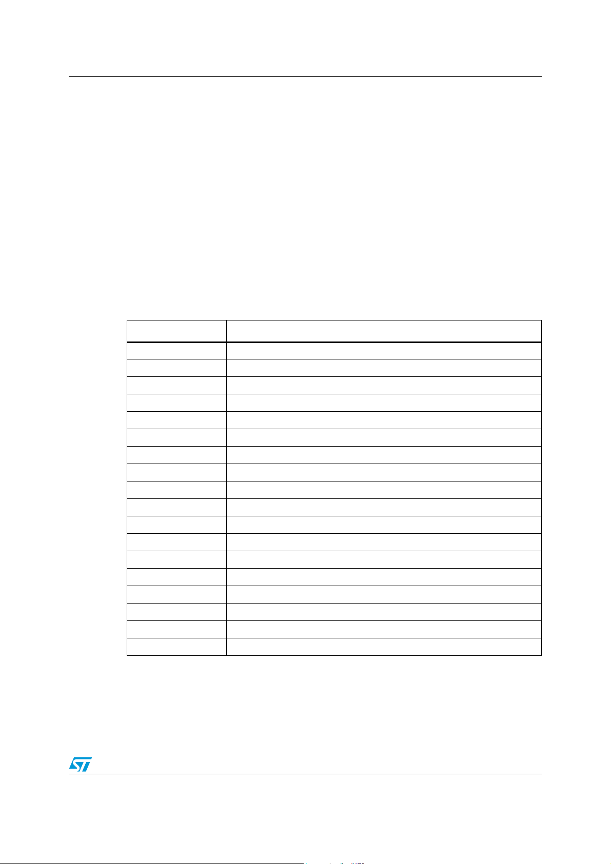
AN3995 Further information
Appendix C Further information
C.1 Reference document
1. SPC564Bxx, SPC56ECxx 32-bit MCU family built on the Power Architecture® for
automotive body electronics applications (SPC564Bxx, SPC56ECxx datasheet, Doc ID
17478)
2. SPC564Bxx, SPC56ECxx 32-bit MCU family built on the embedded Power
Architecture
C.2 Acronyms and abbreviations
A short list of acronyms and abbreviations used in this document is reported in (Section C.1:
Reference document) for completeness.
Table 5. Acronyms and abbreviations
Terms Meanings
BAM Boot assist module
CR Control register
®
(SPC564Bxx, SPC56ECxx RM0070 Doc ID 18196)
DMA Direct memory access
ECC Error correcting code
GPIO General purpose input/output
MC_CGM Clock generation module
MC_ME Mode entry
MCM Miscellaneous control module
MMU Memory management unit
MPU Memory protection unit
NVM Not-volatile memory
PLL Phase locked loop
SoC System on chip
SoR Sphere of replication
SSCM System status and configuration module
ST STMicroelectronics
SWT Software watchdog timer
TLB Translation lookaside buffer
Doc ID 022384 Rev 1 47/49
Page 48

Revision history AN3995
Revision history
Table 6. Document revision history
Date Revision Changes
10-Nov-2011 1 Initial release.
48/49 Doc ID 022384 Rev 1
Page 49

AN3995
Please Read Carefully:
Information in this document is provided solely in connection with ST products. STMicroelectronics NV and its subsidiaries (“ST”) reserve the
right to make changes, corrections, modifications or improvements, to this document, and the products and services described herein at any
time, without notice.
All ST products are sold pursuant to ST’s terms and conditions of sale.
Purchasers are solely responsible for the choice, selection and use of the ST products and services described herein, and ST assumes no
liability whatsoever relating to the choice, selection or use of the ST products and services described herein.
No license, express or implied, by estoppel or otherwise, to any intellectual property rights is granted under this document. If any part of this
document refers to any third party products or services it shall not be deemed a license grant by ST for the use of such third party products
or services, or any intellectual property contained therein or considered as a warranty covering the use in any manner whatsoever of such
third party products or services or any intellectual property contained therein.
UNLESS OTHERWISE SET FORTH IN ST’S TERMS AND CONDITIONS OF SALE ST DISCLAIMS ANY EXPRESS OR IMPLIED
WARRANTY WITH RESPECT TO THE USE AND/OR SALE OF ST PRODUCTS INCLUDING WITHOUT LIMITATION IMPLIED
WARRANTIES OF MERCHANTABILITY, FITNESS FOR A PARTICULAR PURPOSE (AND THEIR EQUIVALENTS UNDER THE LAWS
OF ANY JURISDICTION), OR INFRINGEMENT OF ANY PATENT, COPYRIGHT OR OTHER INTELLECTUAL PROPERTY RIGHT.
UNLESS EXPRESSLY APPROVED IN WRITING BY TWO AUTHORIZED ST REPRESENTATIVES, ST PRODUCTS ARE NOT
RECOMMENDED, AUTHORIZED OR WARRANTED FOR USE IN MILITARY, AIR CRAFT, SPACE, LIFE SAVING, OR LIFE SUSTAINING
APPLICATIONS, NOR IN PRODUCTS OR SYSTEMS WHERE FAILURE OR MALFUNCTION MAY RESULT IN PERSONAL INJURY,
DEATH, OR SEVERE PROPERTY OR ENVIRONMENTAL DAMAGE. ST PRODUCTS WHICH ARE NOT SPECIFIED AS "AUTOMOTIVE
GRADE" MAY ONLY BE USED IN AUTOMOTIVE APPLICATIONS AT USER’S OWN RISK.
Resale of ST products with provisions different from the statements and/or technical features set forth in this document shall immediately void
any warranty granted by ST for the ST product or service described herein and shall not create or extend in any manner whatsoever, any
liability of ST.
ST and the ST logo are trademarks or registered trademarks of ST in various countries.
Information in this document supersedes and replaces all information previously supplied.
The ST logo is a registered trademark of STMicroelectronics. All other names are the property of their respective owners.
© 2011 STMicroelectronics - All rights reserved
STMicroelectronics group of companies
Australia - Belgium - Brazil - Canada - China - Czech Republic - Finland - France - Germany - Hong Kong - India - Israel - Italy - Japan -
Malaysia - Malta - Morocco - Philippines - Singapore - Spain - Sweden - Switzerland - United Kingdom - United States of America
www.st.com
Doc ID 022384 Rev 1 49/49
 Loading...