


AN3973
Application note
Electronic ballast with active PFC using
STD3N62K3 power MOSFET and STD845DN40 BJT device
Introduction
In the most recent developments regarding energy saving, optimization and correct
selection of design components are considered a must in order to have improved electric
efficiency. An increasing sensitivity regarding energy problems has made companies and
consumers more demanding. In this context, cooperation and support between silicon
makers and customers is paramount: an exchange of experience leads to a better and
quicker way to realize new projects. In this article, we present an electronic ballast project
designed thanks to customer input. This application note describes the demonstration board
for 2X28 W electronic lamp ballast with active PFC. The ballast is formed by a part of the
PFC section and a self-oscillating half bridge converter. The circuit has been designed for a
nominal input voltage of 230 Vrms±15% and 50-60 Hz. The key components are the power
bipolar transistor (STD845DN40), the MOSFET device (STD3N62K3), and an ST power
switching driver for the PFC section. The purpose of this application note is to show a simple
and cheap lighting application optimized in terms of power factor (PFC), THD harmonic
distortion, and electric efficiency. The DC-AC converter section presents a layout solution
that offers the customer the possibility of using a bipolar transistor, or DIP 8 or SOT-82
package.
November 2011 Doc ID 022164 Rev 1 1/24
www.st.com

Contents AN3973
Contents
1 System description . . . . . . . . . . . . . . . . . . . . . . . . . . . . . . . . . . . . . . . . . . 4
2 Power factor section . . . . . . . . . . . . . . . . . . . . . . . . . . . . . . . . . . . . . . . . . 5
2.1 PFC section design . . . . . . . . . . . . . . . . . . . . . . . . . . . . . . . . . . . . . . . . . . 6
2.1.1 Input capacitor . . . . . . . . . . . . . . . . . . . . . . . . . . . . . . . . . . . . . . . . . . . . . 7
2.1.2 Output capacitor . . . . . . . . . . . . . . . . . . . . . . . . . . . . . . . . . . . . . . . . . . . 7
2.1.3 Boost inductor . . . . . . . . . . . . . . . . . . . . . . . . . . . . . . . . . . . . . . . . . . . . . 7
2.1.4 Power MOSFET selection . . . . . . . . . . . . . . . . . . . . . . . . . . . . . . . . . . . . 7
2.1.5 L6562A biasing circuitry . . . . . . . . . . . . . . . . . . . . . . . . . . . . . . . . . . . . . . 8
3 DC-AC converter . . . . . . . . . . . . . . . . . . . . . . . . . . . . . . . . . . . . . . . . . . . 10
3.1 System description . . . . . . . . . . . . . . . . . . . . . . . . . . . . . . . . . . . . . . . . . . 11
3.1.1 Preheating phase . . . . . . . . . . . . . . . . . . . . . . . . . . . . . . . . . . . . . . . . . . 11
3.1.2 Ignition phase . . . . . . . . . . . . . . . . . . . . . . . . . . . . . . . . . . . . . . . . . . . . 12
3.1.3 Steady-state phase . . . . . . . . . . . . . . . . . . . . . . . . . . . . . . . . . . . . . . . . 13
4 Driving optimization . . . . . . . . . . . . . . . . . . . . . . . . . . . . . . . . . . . . . . . . 14
4.1 MOSFET circuit optimization . . . . . . . . . . . . . . . . . . . . . . . . . . . . . . . . . . 14
4.2 BJT circuit optimization . . . . . . . . . . . . . . . . . . . . . . . . . . . . . . . . . . . . . . 16
5 Experimental results . . . . . . . . . . . . . . . . . . . . . . . . . . . . . . . . . . . . . . . . 18
6 Conclusions . . . . . . . . . . . . . . . . . . . . . . . . . . . . . . . . . . . . . . . . . . . . . . . 19
7 Layout layers . . . . . . . . . . . . . . . . . . . . . . . . . . . . . . . . . . . . . . . . . . . . . . 20
8 Bill of material . . . . . . . . . . . . . . . . . . . . . . . . . . . . . . . . . . . . . . . . . . . . . 21
9 Reference . . . . . . . . . . . . . . . . . . . . . . . . . . . . . . . . . . . . . . . . . . . . . . . . . 22
10 Revision history . . . . . . . . . . . . . . . . . . . . . . . . . . . . . . . . . . . . . . . . . . . 23
2/24 Doc ID 022164 Rev 1

AN3973 List of figures
List of figures
Figure 1. Ballast model . . . . . . . . . . . . . . . . . . . . . . . . . . . . . . . . . . . . . . . . . . . . . . . . . . . . . . . . . . . . 4
Figure 2. PFC section, boost converter diagram . . . . . . . . . . . . . . . . . . . . . . . . . . . . . . . . . . . . . . . . . 5
Figure 3. Inductor and input current waveform. MOSFET timing . . . . . . . . . . . . . . . . . . . . . . . . . . . . 6
Figure 4. PFC section, relevant elements for THD and PFC factor . . . . . . . . . . . . . . . . . . . . . . . . . . . 8
Figure 5. DC-AC converter section . . . . . . . . . . . . . . . . . . . . . . . . . . . . . . . . . . . . . . . . . . . . . . . . . . 10
Figure 6. Voltage and current lamp waveforms . . . . . . . . . . . . . . . . . . . . . . . . . . . . . . . . . . . . . . . . . 12
Figure 7. Zoom of the highlighted section (in Figure 6) . . . . . . . . . . . . . . . . . . . . . . . . . . . . . . . . . . . 12
Figure 8. Voltage and current lamp waveforms . . . . . . . . . . . . . . . . . . . . . . . . . . . . . . . . . . . . . . . . . 12
Figure 9. Zoom of the highlighted section (in Figure 8) . . . . . . . . . . . . . . . . . . . . . . . . . . . . . . . . . . . 12
Figure 10. Voltage and current lamp waveforms . . . . . . . . . . . . . . . . . . . . . . . . . . . . . . . . . . . . . . . . . 13
Figure 11. Zoom of the highlighted section (in Figure 10) . . . . . . . . . . . . . . . . . . . . . . . . . . . . . . . . . . 13
Figure 12. Snubber and driving circuit of MOSFET . . . . . . . . . . . . . . . . . . . . . . . . . . . . . . . . . . . . . . . 14
Figure 13. MOSFET turn-off without snubber circuit . . . . . . . . . . . . . . . . . . . . . . . . . . . . . . . . . . . . . . 15
Figure 14. MOSFET turn-off with snubber circuit . . . . . . . . . . . . . . . . . . . . . . . . . . . . . . . . . . . . . . . . . 15
Figure 15. MOSFET turn-on @ R7=10 W . . . . . . . . . . . . . . . . . . . . . . . . . . . . . . . . . . . . . . . . . . . . . . 15
Figure 16. MOSFET turn-on R7=47 W . . . . . . . . . . . . . . . . . . . . . . . . . . . . . . . . . . . . . . . . . . . . . . . . 15
Figure 17. BJT in low side. Snubber and driving circuit of BJT . . . . . . . . . . . . . . . . . . . . . . . . . . . . . . 16
Figure 18. Steady-state operation . . . . . . . . . . . . . . . . . . . . . . . . . . . . . . . . . . . . . . . . . . . . . . . . . . . . 16
Figure 19. Zoom of the highlighted section 1 (in Figure 18) . . . . . . . . . . . . . . . . . . . . . . . . . . . . . . . . 17
Figure 20. Zoom of the highlighted section 2 (in Figure 18) . . . . . . . . . . . . . . . . . . . . . . . . . . . . . . . . 17
Figure 21. Bottom layout layer . . . . . . . . . . . . . . . . . . . . . . . . . . . . . . . . . . . . . . . . . . . . . . . . . . . . . . . 20
Figure 22. Top layout layer . . . . . . . . . . . . . . . . . . . . . . . . . . . . . . . . . . . . . . . . . . . . . . . . . . . . . . . . . 20
Figure 23. Silkscreen top . . . . . . . . . . . . . . . . . . . . . . . . . . . . . . . . . . . . . . . . . . . . . . . . . . . . . . . . . . . 20
Figure 24. Silkscreen bottom . . . . . . . . . . . . . . . . . . . . . . . . . . . . . . . . . . . . . . . . . . . . . . . . . . . . . . . . 20
Doc ID 022164 Rev 1 3/24
System description AN3973
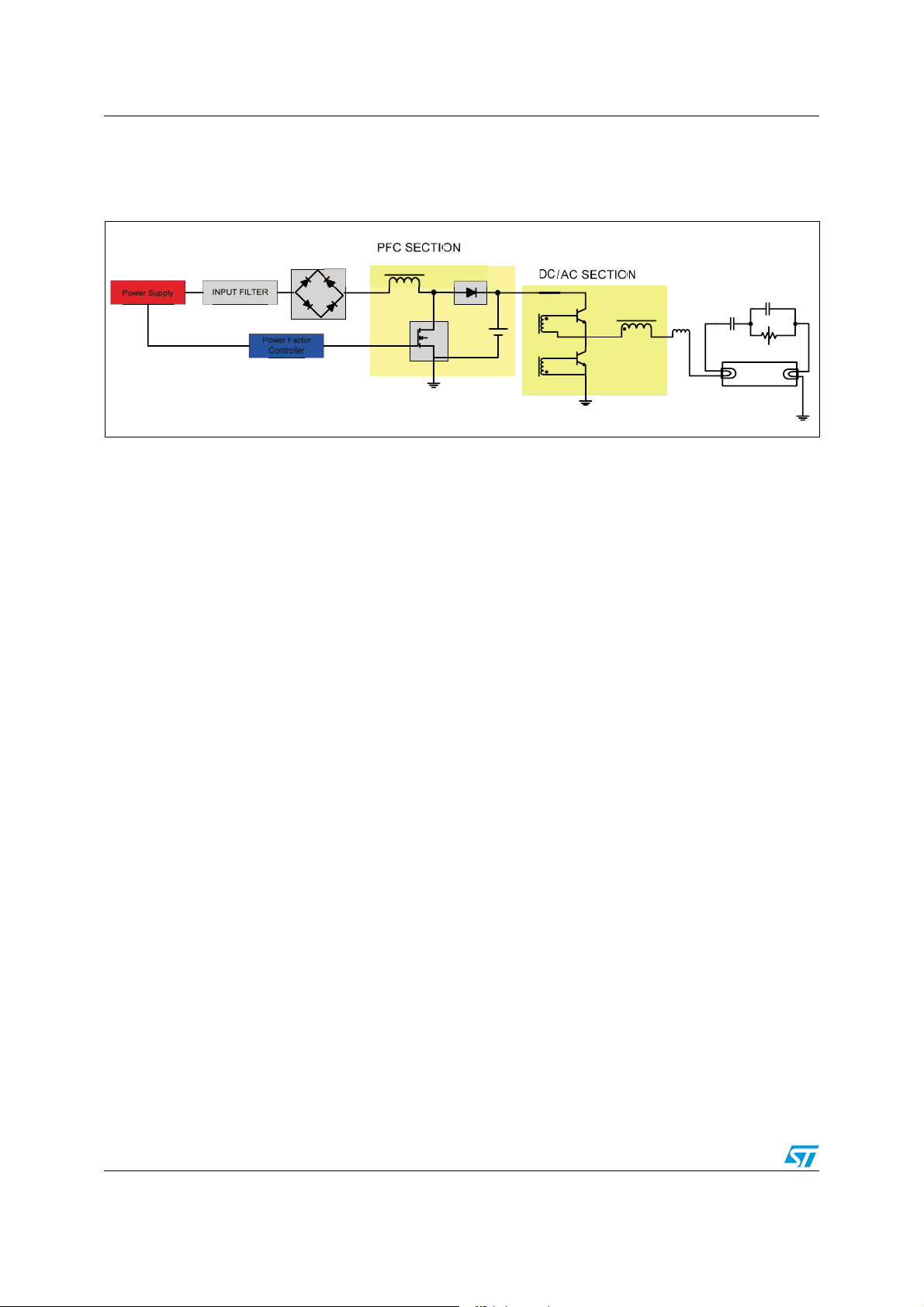
1 System description
Figure 1. Ballast model
!-V
The system description is subdivided into two main sections, namely the PFC boost section
and half bridge converter. The system description starts with the PFC section and then
continues with the DC-AC converter. In the PFC section the method and the electrical
elements concerning the optimization of PFC and THD parameters are pointed out. In the
DC-AC converter section, the focus is the optimization of transistor bipolar driving.
4/24 Doc ID 022164 Rev 1
AN3973 Power factor section
2 Power factor section
The PFC section (boost converter) mainly consists of STD3N62K3 MOSFET SuperMESH3
technology and the L6562A power switching driver. The new SuperMESH3 technology is
obtained through the combination of fine tuning between standard SuperMESH and
MDMESH technology. This has resulted in the development of a new technology that
represents the optimization of the basic standard SuperMESH in terms of R
dynamic features. SuperMesh has integrated Zener diodes gate-to-source in order to
protect its gate-oxide from voltage spikes. The L6562A is a current-mode PFC controller
operating in transition mode. It has an improved performance compared to its predecessor,
the L6561.
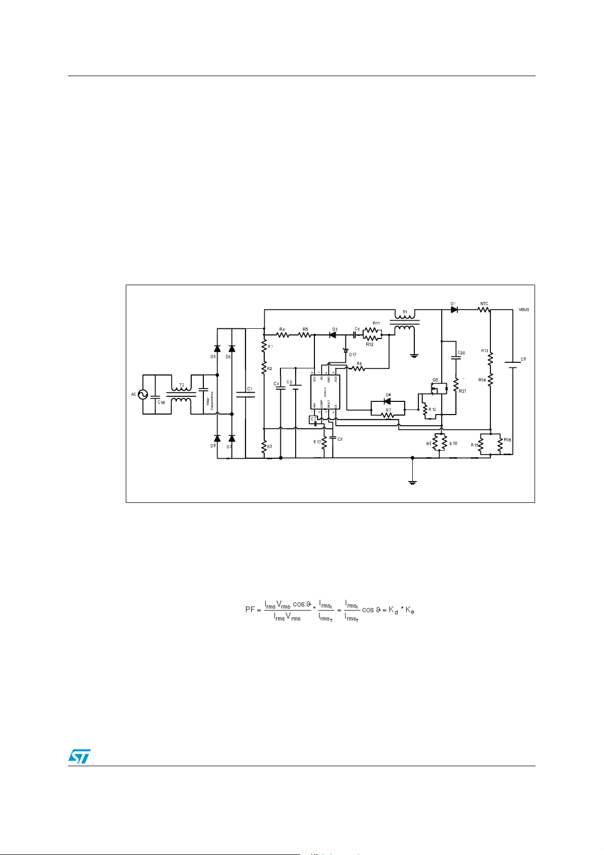
Figure 2 shows the PFC section schematic plus the component values.
Figure 2. PFC section, boost converter diagram
DS(on)
* area and
!-V
The power factor consists of the displacement factor related to phase angle and the
distortion factor related to wave shape. The displacement factor is the ratio between the real
power (transferred to the output) and the apparent power (RMS line voltage times RMS line
current) drawn from the main, while the distortion factor is the ratio between the
fundamental component of the current and the total current:
Equation 1
Therefore, the section is designed in order to minimize input current distortion and forces the
input current to be in phase with the input voltage.
This system operates in transition mode, the boundary between continuous and
discontinuous current mode. The control simplicity and the inductor size, due to the low
inductance value needed, are the main advantages of this conduction current mode.
Doc ID 022164 Rev 1 5/24
Power factor section AN3973
2.1 PFC section design
The first step is to define the converter specifications that the user must set for the new PFC
boost topology project.
Table 1. Converter specification data and fixed parameters
Name Symbol Value
Input voltage range V
Nominal output voltage V
Nominal output power P
INmin-VINmax
out
out
Target efficiency n ∼
Minimum switching frequency f
s
180 Vac to 264 Vac
400 V
60 W
90%
35 kHz
Expected power factor PF 0.99
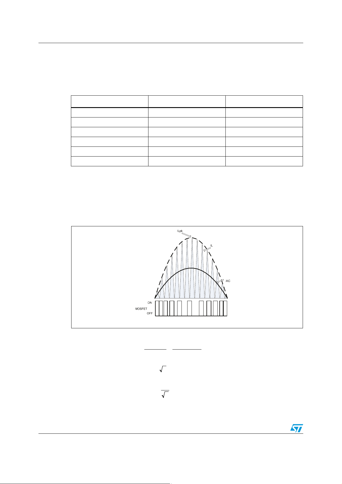
At switching frequency, the inductor current is a triangle shape and the average value is half
of the peak of triangle. The resulting inductor current is shown in Figure 3, where it is also
shown that, by geometric relationships, the average value is the peak of sinewave input
current. The system operates the boundary between continuous and discontinuous
(transition mode current):
Figure 3. Inductor and input current waveform. MOSFET timing
Therefore the main operating conditions are:
● RMS input current
● Peak inductor current
● RMS inductor current
6/24 Doc ID 022164 Rev 1
I
in
P
IL =
P
in
==
PFV
minAC
I22IL =
inpk
2
3
out
η
minAC
I
inRMS
AM10586v1
A374.0
=
PFV*

AN3973 Power factor section
2.1.1 Input capacitor
The input filter capacitor (Cin) must reduce the high frequency voltage ripple across Cin and
the switching noise due to the high frequency inductor current ripple. The input capacitor
depends on the voltage ripple (r) and it is usually between 5% and 20% of the minimum
input voltage:
● Ripple voltage coefficient (%):
● Input capacitor
=
C
IN
π
1.0r =
I
in
r*V*f2
minACminSW
nF100
≈
In the applicative conditions, a polyester capacitor was chosen. It offers benefits in terms of
voltage stability and power factor (PF).
2.1.2 Output capacitor
The output capacitor is a function of voltage ripple (ΔV
ΔV
is usually selected at around 1.5% of the output voltage capacitor:
out
● Output capacitor
An electrolytic capacitor has been selected because it has low impedance (ESR) and
therefore provides good energy storage and improves the transient performance.
2.1.3 Boost inductor
The inductor boost depends on the several parameters and different approaches which can
be used. First, the inductor value is usually calculated so that the minimum switching
frequency is greater than the maximum frequency of the L6562A internal starter. Assuming
unity PF, it is possible to write:
● Instantaneous switching frequency
Therefore, the inductor value is determined at the top of the sinusoid ( ) where the
switching frequency is the minimum:
● Inductor value
The optimum dynamic performances of the MOSFET device, selected for this application,
have allowed higher operation minimum frequency and consequently lower boost
inductance. In this case a 1.8 mH boost inductance was selected.
) and of the capacitor impedance.
out
C
=
Out
)V(L
=
AC
2
AC
P
out
−
VV*f4
Δπ
fθ−=
sw
outoutmain
P*Vf2
uF47
≈
2
1
AC
LP2
IN
)V2V(V
ACOut
INoutminSW
ACOut
V
out
))sin(V2V(V
π
=θ
2
2.1.4 Power MOSFET selection
MOSFET SuperMESH3 technology perfectly matches boost converter characteristics. In
fact, this technology has got a dynamic performance better than that of the standard
SuperMESH but not as good as MDMESH. That translates into having low switching power
losses and commutation which is not so fast that it implies ringing phenomenon such as
decreased PF and THD factors. MOSFET selection is based mainly on maximum voltage
rating, total power losses, and maximum operating temperature. In this case a MOSFET
device with minimum voltage rating 500 V (1.2*V
Doc ID 022164 Rev 1 7/24
=480 V) must be selected: 20% of V
BUS
BUS

Power factor section AN3973
indicates the safe margin. In the end, the MOSFET selection depended on power losses
and maximum operating temperature. MOSFET total power losses depend on conduction
and switching losses. The conduction losses at minimum input voltage are calculated by:
● Conduction losses
● RMS switch current
Pc R
DS on()
2
I
⋅=
SWrms
senV2V
min
θ−
*senII
θ=
LpkSWrms
V3
inBUS
BUS
The switching losses in the MOSFET occur only during turn-off, because this boost topology
works in transition mode. Basically they can be expressed by:
● Switching power losses
Psw
where Qgd is the gate drain charge, I
f
s(ILRMS
) is switch frequency calculated for value.
=
is RMS inductor current, Ig is the gate current and
LRMS
I*V*Q
LBUSgd
RMS
I*2
g
)I(f
Ls
RMS
Based on the information above, the MOSFET choice was the STD3N62K3 device. The final
results show that STD3N62K3 ensures good performance in terms of electrical and thermal
behavior.
2.1.5 L6562A biasing circuitry
The dimensioning of biasing circuitry of the L6562A driver is reported for only a few
elements. In particular, the dimensioning is shown for those components that have been
relevant in terms of THD harmonic distortion and power factor (PF).
Figure 4. PFC section, relevant elements for THD and PFC factor
!-V
Pin2 (COMP). A feedback compensation network is put between this pin and INV in order to
fix narrow bandwidth and avoid high distortion of the input current waveform. In this way a
8/24 Doc ID 022164 Rev 1

AN3973 Power factor section
voltage value (VCOMP) is determined, it is the reference (in the multiplier characteristic
graph) for the “MULT” and “CS” signal. Taking this into account, the procedure to set the
operation point of the multiplier Pin3 (MULT) is suggested. First, the maximum peak value is
selected. This value, which occurs at maximum mains voltage, should be less 3 V in case of
single mains. Therefore:
● Minimum peak value:
● This value is then multiplied by the minimum guaranteed and it gives
the maximum output voltage of multiplier: .
● In this way the divider resistor is: .
● Subsequently thanks to these relationships:
V
minCS
R <
S
IL
.
peak
VV =
MULTpk xminMU LTpk
R
3
V
V
=
RRR
++
321
V
MULTpkx
V*2
minINRMS
maxINRMS
V
Δ
CS
V
Δ
MULT
V*1.1V =
maxINRMS
1.1
=
minMULTpkxCSpk
V)V5.2V(kV −=
MULTCOMPCS
The divider resistor R3=15 kΩ and R1/R2=2.7 MΩ and the sense resistors R9=0.39 Ω and
R10=1 Ω have been fixed.
In particular:
– the reference for the current sense.
– the typical multiplier gain
– the voltage on the Pin2
– the voltage on the Pin3
This experimental fine tuning guarantees a high value of both PF and THD.
Pin5 (ZCD).This pin is the zero current detector circuit. In this case (PFC in transition mode)
the ZCD pin is connected, through a resistor, to the auxiliary winding of the boost inductor.
In particular, the resistance value (R6=47 kΩ) was tuned in order to minimize the switching
power losses at turn-on. In fact, this fine tuning allows the MOSFET to switch on when the
resonant phenomenon between boost inductor and drain-source capacitance occurs on the
valley of the drain voltage. In this way, the MOSFET device turns on with lower voltage
across drain source, this implies a reduced current peak and lower switch-on losses.
Doc ID 022164 Rev 1 9/24

DC-AC converter AN3973
3 DC-AC converter
The electronic ballast consists of a self-oscillating voltage-fed half bridge inverter, which has
been developed to drive two lamps of 28 W. One of the key components is the
STD845DN40 power bipolar transistor. It is a dual NPN high voltage power transistor and is
housed in dual-island DIP-8 package. This package solution allows to save layout area and
its driving circuit has been optimized so that the thermal performance is not too different to
that of a single transistor. The second of the key components is the possibility to use, for
bipolar transistors, a DIP-8 or SOT-82 package solution.
Figure 5. DC-AC converter section
!-V
The DC-AC converter section has been realized according to customer indications. The
ballast coil L3/L5 (3.7 mH) and the saturable core transformer L4 (20 µH) were given by the
customer and in relation to this, all the other passive and active elements have been
selected. In particular, the design has been realized so that the lamp voltage is 180 V and
the lamp current about 0.15 A. The following design procedure is suggested for resonant
components and for proper operation of the self-oscillating inverter.
Considering first the given set of specifications: V
=400 V, output current I
BUS
OUT
=0.15 A,
ballast coil L3/L5=3.7 mH, core saturable transformer L4=20 µH and, more specifically, the
lamp resistance (R ≈1160 Ω).
The RMS input voltage can be calculated from:
Equation 2
=2VV
BUSRMS_IN
π
The value of the desired characteristic impedance is extracted:
10/24 Doc ID 022164 Rev 1

AN3973 DC-AC converter
Equation 3
Z ==
r
L
C
I
OUT
RMS_IN
V
Given the resonance inductance, the switching frequency is calculated:
Equation 4
Z
f
s
r
=
3L2
π
Then the resonant capacitor is given by:
Equation 5
Cπ=
r
1
Z*f2
rs
where .
r
11C10CC
+=
For proper operation resonant, the network must be , in this way the
drop across the serially connected lamps is higher than the bus voltage and the current is
sinusoidal. This is the preferred operation mode.
3.1 System description
The system description is subdivided into three main sections, preheating, ignition and
steady-state phase.
3.1.1 Preheating phase
To obtain a long lamp life, it is important that the electrodes are preheated by a certain
current. A PTC RT1 (for the single lamp) put in parallel with the lamp guarantees the
electrode preheating as it ensures that the current is flowing via the lamp electrodes. During
this period the voltage across the lamp is maintained sufficiently low to avoid the lamp
igniting too early and the operating frequency is determined by L3 and C11 (C10 is partially
inhibited by PTC).
R
1
Q
>=
Z
r
Doc ID 022164 Rev 1 11/24

DC-AC converter AN3973
Figure 6. Voltage and current lamp
waveforms
The preheating time depends on the setting of the circuit parallel to the lamp (time
constant). In particular, it is the PTC value that determines this duration of preheating as
well as the ignition of the lamp. In fact, as long as it does not increase its impedance, it does
not allow the resonant circuit (L3, C11, and C10) to generate the overvoltage on the lamp
and so on the ignition itself.
3.1.2 Ignition phase
Figure 7. Zoom of the highlighted section (in
Figure 6)
As soon as the electrodes are preheated, the impedance of the PTC rapidly increases and
the series resonance of L3, C11, and C10 results in an increasing lamp voltage. The lamp
voltage increases until it ignites.
Figure 8. Voltage and current lamp
waveforms
The resonant circuit operates in order to ignite the lamp. In the ignition phase, the voltage
shape of the lamp depends on the rise time of the PTC impedance.
Figure 9. Zoom of the highlighted section (in
Figure 8)
12/24 Doc ID 022164 Rev 1

AN3973 DC-AC converter
Resonant circuit frequency:
Equation 6
f
=
r
1
)CC(L2
+π
10103
3.1.3 Steady-state phase
Once the tubes are ionized, it is effectively a short-circuit across C10 + C11. The inverter
system sets the voltage and current shape so that the lamp correctly operates.
Figure 10. Voltage and current lamp
waveforms
Therefore, the frequency is defined by C15 and so is lower than the ignition phase. At this
frequency, the overvoltage generated is also lower, but enough to keep the tube lit. During
steady-state, when the transistor is first turned on, the current in the transformer L4
increases until its core saturates. At this point, after the storage time of the transistor has
passed, it turns off. In this way, the operating frequency also depends on the size and
maximum flux density of the core of L4 and the storage times of the transistor.
Figure 11. Zoom of the highlighted section (in
Figure 10)
Doc ID 022164 Rev 1 13/24

Driving optimization AN3973
4 Driving optimization
The driving circuit optimization has been done in order to have the best performance of the
lighting system. Basically, this circuit concerns MOSFET and BJT transistors and it has
been realized in order to have thermal and electrical behavior of devices compliant to the
system features.
4.1 MOSFET circuit optimization
The elements of circuit optimization are shown below.
Figure 12. Snubber and driving circuit of MOSFET
&
4
'
5
5
5
5 5
!-V
A small RC snubber circuit (C=680 pF and R=180 Ω) has been used to prevent voltage
spikes and voltage oscillation across the MOSFET during device turn-off. This means
limiting the rate of rise (ΔV
/Δt) of the MOSFET, to reduce the cross between voltage and
DS
current and to have less switching losses during turn-off. The driving circuit (R7=47 Ω and
diode) allows the MOSFET to not turn on too quickly in order to reduce the discharge of
snubber circuit capacitance and consequently to guarantee negligible switch-on losses and,
thanks to the diode, it allows the fastest discharge of parasitic capacitance of the MOSFET
and therefore speeds up switch-off.
14/24 Doc ID 022164 Rev 1

AN3973 Driving optimization
The waveforms show the advantages of the driving solution and the snubber circuit.
Figure 13. MOSFET turn-off without snubber
circuit
Figure 14. MOSFET turn-off with snubber
circuit
The comparison between these waveforms shows that the insertion of the RC snubber
circuit reduces voltage spikes and Vds slope and in particular it decreases switching losses
during turn-off.
Figure 15. MOSFET turn-on @ R7=10 Ω Figure 16. MOSFET turn-on R7=47 Ω
As the figures show, the resistor R7=47 Ω in the driving circuit provides a slower switch-on
of the MOSFET, reduces the discharge of snubber circuit capacitance and consequently it
guarantees negligible power losses during turn-on.
Doc ID 022164 Rev 1 15/24

Driving optimization AN3973
4.2 BJT circuit optimization
The snubber and the driving circuit of BJT is the same as low side and high side. In
particular,
Figure 17. BJT in low side. Snubber and driving circuit of BJT
Figure 6 shows the elements of low side BJT driving circuit which are highlighted.
'
5
4
5
&
&
5
!-V
A small C9 snubber circuit has been used in order to decrease the cross between voltage
(VCE) and current (ICE) and, consequently, to have less switching losses during turn-off.
The capacitance C9 allows to limit, in the middle point (2), the rate of rise of VCE. This
snubber capacitance is put in the low side in order to ensure the discharge to ground and
therefore to avoid a current too high spike during the startup phase. The choice of the C9
capacitance was made in order to balance the power switching losses, in fact, the value
C9=680 pF, obtained in experimental results, guaranteed the lowest switch-off losses and
negligible switch-on losses due to the discharge of capacitance during the turn-on of the
transistor. The driving circuit (R23=5.6 Ω, R24=33 Ω and diode) provided the best
commutation of the bipolar transistor. The R24 value was able to reduce current spike due to
the discharge of snubber circuit capacitance and to ensure the charge quantity so that the
IC current was sufficient to power the lamp. R23||R24 put in parallel determined the
commutation time, the storage time of the bipolar transistor, and consequently the operating
frequency of the ballast system.
The waveforms in
Figure 18 show the behavior of BJT during steady-state operation.
Figure 18. Steady-state operation
1
16/24 Doc ID 022164 Rev 1
2

AN3973 Driving optimization
Figure 19. Zoom of the highlighted section 1
(in Figure 18)
The turn-on of the bipolar transistor had a spike of Ibe current due to C18 capacitance, it
assisted the charge phenomenon of the bipolar junction. The fall time value during the
turn-off was very low and this implied shorter commutation time and lower switching losses.
Figure 20. Zoom of the highlighted section 2
(in Figure 18)
Doc ID 022164 Rev 1 17/24

Experimental results AN3973
5 Experimental results
The experimental results have been measured for different input voltage levels and leaving
the application in free air: all electrical components were in the original position. The test
equipment list has been given in order to check the measurements repeatability.
● Input voltage: ∼180 - 230 - 265 Vac
● Test equipment:
– Agilent AC power supply 6813B
– Digital power meter WT210
– Flir systems thermal camera
● Ambient temperature:
– ∼25 °C
Table 2. Main electrical and thermal results @ 25 °C ambient temperature
Input voltage [V] PFC THD Pin [W] MOSFET temperature [°C]
180 V 0.998 3.5 66.4 52 78
230 V 0.993 4.1 65.4 43 78
264 V 0.983 13.9 65.8 42 78
BJT temperature [°C] @
DIP-8
Exchanging input voltage, the main electrical parameters of the PFC factor and THD
suggest that the application performances were very good. Everything the energy soaked
up by the system was converted into useful power. The temperatures of transistor devices
respect the datasheet specifications. In particular the temperature of BJT transistors was
not too high considering that the DIP-8 package had a dual NPN high voltage power
transistor housed in dual-island.
Tab l e 3 , the thermal performance between the DIP-8 and SOT-82 package were
In
compared.
Table 3. Thermal results @ 25 °C ambient temperature
Input voltage [V] BJT temperature [°C] @ DIP-8 BJT temperature [°C] @ SOT-82
230 V 78 61
The temperature of the two package solutions was not too different, for both cases the
transistors worked in safety condition. The temperature value of the bipolar transistor didn't
depend on the input voltage because the PFC active section allows to fix, at 400Vdc, the
voltage of the DC-AC section. For this reason the temperature of the bipolar (both
packages), was only measured at 230 Vac (nominal input voltage).
18/24 Doc ID 022164 Rev 1

AN3973 Conclusions
6 Conclusions
The proposed design of electrical ballast with active PFC and self-oscillating inverter
showed the capability of driving 2X28 W fluorescent lamps with very good electrical and
thermal performance. The component choice and the optimization of the transistors driving
circuit guarantee the highest PFC factor and lowest THD. For each work condition the
ballast drove the lamps safely.
This power source offers the customer the double package solution: bipolar transistors in
DIP-8 or SOT-82 package. For both solutions the temperature of power devices is fully
compliant with the absolute maximum rating limit in the datasheet specification.
In addition, the design layout was designed using the double layer solution. Anyway,
according to customer needs, the PCB layout of the application can be realized both in
double layer and in single, using the jumpers instead of the net in the top layer.
Doc ID 022164 Rev 1 19/24

Layout layers AN3973
7 Layout layers
Figure 21. Bottom layout layer
Figure 22. Top layout layer
Figure 23. Silkscreen top
Figure 24. Silkscreen bottom
20/24 Doc ID 022164 Rev 1

AN3973 Bill of material
8 Bill of material
Table 4. Bill of material
Quantity Reference Part/value
2 R1/R2 2.7 MΩ
1R315 kΩ
2 R4/R5 270 kΩ
1R647 kΩ
1 R7 10 Ω
1 R12 47 kΩ
1R90.39 Ω
1R101 Ω
2 R11/R12 220 Ω
2 R13/R14 1 MΩ
1 R15 15 kΩ
1 R16 82 kΩ
1 R17 10 kΩ
3 R18/R19/R20 180 kΩ
2 R21/R23 5.6 Ω
2 R22/R24 33 Ω
2 R25/R26 0.82 Ω
1 R27 180 Ω
1C1150 nF
4 C2/C5/C17/C18 10 nF
1 C3 10 µF
2 C4/C8 100 nF
1 C6 33 µF
1C71 µF
1 C21 680 pF
2 C10/C12 4.7 nF
2 C11/C13 10 nF
2 C14/C15 100 nF
1 C20 27 pF
1 C19 330 nF
1 Filter capacitance 2.2 nF
1 D1 STTH1L06A
Doc ID 022164 Rev 1 21/24

Reference AN3973
Table 4. Bill of material (continued)
Quantity Reference Part/value
4 D3/D4/D12/D13 1N4148
5 D5/D6/D7/D8/D11 1N4007
1D16Zener
2RT1/RT2PTC
1 NTC 2.5
1 T2 18 mH filter inductance
1 T1 1.8 mH 0.5 A
1 L4 20 µH
2 L3/L5 3.7 mH
1 U3 L6562A
1 Q1 STD3N62K3
1 Q8 1-2 bipolar STD845DN40
9 Reference
1. AN2761 application note
22/24 Doc ID 022164 Rev 1

AN3973 Revision history
10 Revision history
Table 5. Document revision history
Date Revision Changes
11-Nov-2011 1 Initial release.
Doc ID 022164 Rev 1 23/24

AN3973
Please Read Carefully:
Information in this document is provided solely in connection with ST products. STMicroelectronics NV and its subsidiaries (“ST”) reserve the
right to make changes, corrections, modifications or improvements, to this document, and the products and services described herein at any
time, without notice.
All ST products are sold pursuant to ST’s terms and conditions of sale.
Purchasers are solely responsible for the choice, selection and use of the ST products and services described herein, and ST assumes no
liability whatsoever relating to the choice, selection or use of the ST products and services described herein.
No license, express or implied, by estoppel or otherwise, to any intellectual property rights is granted under this document. If any part of this
document refers to any third party products or services it shall not be deemed a license grant by ST for the use of such third party products
or services, or any intellectual property contained therein or considered as a warranty covering the use in any manner whatsoever of such
third party products or services or any intellectual property contained therein.
UNLESS OTHERWISE SET FORTH IN ST’S TERMS AND CONDITIONS OF SALE ST DISCLAIMS ANY EXPRESS OR IMPLIED
WARRANTY WITH RESPECT TO THE USE AND/OR SALE OF ST PRODUCTS INCLUDING WITHOUT LIMITATION IMPLIED
WARRANTIES OF MERCHANTABILITY, FITNESS FOR A PARTICULAR PURPOSE (AND THEIR EQUIVALENTS UNDER THE LAWS
OF ANY JURISDICTION), OR INFRINGEMENT OF ANY PATENT, COPYRIGHT OR OTHER INTELLECTUAL PROPERTY RIGHT.
UNLESS EXPRESSLY APPROVED IN WRITING BY TWO AUTHORIZED ST REPRESENTATIVES, ST PRODUCTS ARE NOT
RECOMMENDED, AUTHORIZED OR WARRANTED FOR USE IN MILITARY, AIR CRAFT, SPACE, LIFE SAVING, OR LIFE SUSTAINING
APPLICATIONS, NOR IN PRODUCTS OR SYSTEMS WHERE FAILURE OR MALFUNCTION MAY RESULT IN PERSONAL INJURY,
DEATH, OR SEVERE PROPERTY OR ENVIRONMENTAL DAMAGE. ST PRODUCTS WHICH ARE NOT SPECIFIED AS "AUTOMOTIVE
GRADE" MAY ONLY BE USED IN AUTOMOTIVE APPLICATIONS AT USER’S OWN RISK.
Resale of ST products with provisions different from the statements and/or technical features set forth in this document shall immediately void
any warranty granted by ST for the ST product or service described herein and shall not create or extend in any manner whatsoever, any
liability of ST.
ST and the ST logo are trademarks or registered trademarks of ST in various countries.
Information in this document supersedes and replaces all information previously supplied.
The ST logo is a registered trademark of STMicroelectronics. All other names are the property of their respective owners.
© 2011 STMicroelectronics - All rights reserved
STMicroelectronics group of companies
Australia - Belgium - Brazil - Canada - China - Czech Republic - Finland - France - Germany - Hong Kong - India - Israel - Italy - Japan -
Malaysia - Malta - Morocco - Philippines - Singapore - Spain - Sweden - Switzerland - United Kingdom - United States of America
www.st.com
24/24 Doc ID 022164 Rev 1
 Loading...