

Page 1
Application note
2.0-channel demonstration board
based on the STA381BW and STA381BWS
Introduction
The purpose of this application note is to describe:
■ how to connect the STA381BW/STA381BWS 2.0-channel demonstration board
■ how to evaluate the performance of the demonstration board with significant electrical
curves
■ how to avoid critical issues in the PCB schematic and layout of the
STA381BW/STA381BWS
The STA381BW/STA381BWS demonstration board is configured for 2.0 BTL channels,
releasing up to 2 x 20 W into 8 ohm of power output at 18 V of supply voltage in the VQFN48
package. It represents a total solution for the digital audio power amplifier.
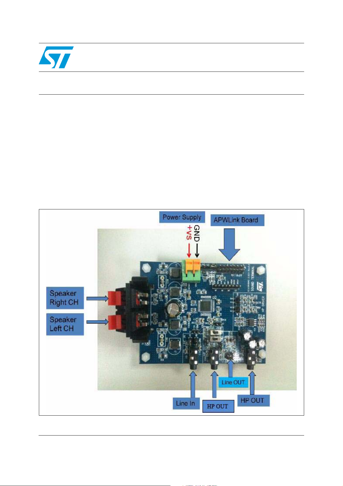
Figure 1. STA381BW/STA381BWS 2.0-channel demonstration board
AN3959
December 2011 Doc ID 022081 Rev 3 1/65
www.st.com
Page 2

Contents AN3959
Contents
1 Functional description of the demonstration board . . . . . . . . . . . . . . . 6
1.1 Connections . . . . . . . . . . . . . . . . . . . . . . . . . . . . . . . . . . . . . . . . . . . . . . . . 6
1.2 Output configuration . . . . . . . . . . . . . . . . . . . . . . . . . . . . . . . . . . . . . . . . . . 6
1.3 Schematic and block diagrams, bill of material, PCB layout . . . . . . . . . . . . 7
2 STA381BWS power section test results . . . . . . . . . . . . . . . . . . . . . . . . 16
3 STA381BW power section test results . . . . . . . . . . . . . . . . . . . . . . . . . 20
4 Analog section test results . . . . . . . . . . . . . . . . . . . . . . . . . . . . . . . . . . 24
5 Thermal performance . . . . . . . . . . . . . . . . . . . . . . . . . . . . . . . . . . . . . . . 26
5.1 Thermal results - test 1 . . . . . . . . . . . . . . . . . . . . . . . . . . . . . . . . . . . . . . 26
5.2 Thermal results - test 2 . . . . . . . . . . . . . . . . . . . . . . . . . . . . . . . . . . . . . . 27
6 Design guidelines for schematic and PCB layout . . . . . . . . . . . . . . . . 28
6.1 Schematic . . . . . . . . . . . . . . . . . . . . . . . . . . . . . . . . . . . . . . . . . . . . . . . . . 28
6.1.1 Criteria for selection of components . . . . . . . . . . . . . . . . . . . . . . . . . . . 28
6.1.2 Decoupling capacitors . . . . . . . . . . . . . . . . . . . . . . . . . . . . . . . . . . . . . . 28
6.1.3 Output filter . . . . . . . . . . . . . . . . . . . . . . . . . . . . . . . . . . . . . . . . . . . . . . 28
6.1.4 Snubber filter . . . . . . . . . . . . . . . . . . . . . . . . . . . . . . . . . . . . . . . . . . . . . 29
6.1.5 Main filter . . . . . . . . . . . . . . . . . . . . . . . . . . . . . . . . . . . . . . . . . . . . . . . . 30
6.1.6 Dumping network . . . . . . . . . . . . . . . . . . . . . . . . . . . . . . . . . . . . . . . . . . 30
6.1.7 Recommended power-up and power-down sequence . . . . . . . . . . . . . 31
6.2 Layout . . . . . . . . . . . . . . . . . . . . . . . . . . . . . . . . . . . . . . . . . . . . . . . . . . . . 31
7 Software setup to use the STA381BW/STA381BWS devices (ST Map)
. . . . . . . . . . . . . . . . . . . . . . . . . . . . . . . . . . . . . . . . . . . . . . . . . . . . . . . . . . 38
7.1 Processing configuration . . . . . . . . . . . . . . . . . . . . . . . . . . . . . . . . . . . . . 38
7.2 STCompressor
TM . . . . . . . . . . . . . . . . . . . . . . . . . . . . . . . . . . . . . . . . . . . . . . . . . . . . . . . 39
7.2.1 STCompressor settings . . . . . . . . . . . . . . . . . . . . . . . . . . . . . . . . . . . . . 41
7.2.2 Configuring and enabling the STCompressor . . . . . . . . . . . . . . . . . . . . 41
7.2.3 Example settings of the STCompressor . . . . . . . . . . . . . . . . . . . . . . . . 42
7.2.4 Test results with APWorkbench . . . . . . . . . . . . . . . . . . . . . . . . . . . . . . . 44
2/65 Doc ID 022081 Rev 3
Page 3

AN3959 Contents
7.3 CRC computation . . . . . . . . . . . . . . . . . . . . . . . . . . . . . . . . . . . . . . . . . . . 45
7.3.1 Biquad CRC computation . . . . . . . . . . . . . . . . . . . . . . . . . . . . . . . . . . . 45
7.3.2 Crossover CRC computation . . . . . . . . . . . . . . . . . . . . . . . . . . . . . . . . . 45
7.3.3 STCompressor
TM
CRC computation . . . . . . . . . . . . . . . . . . . . . . . . . . . 46
7.4 Startup . . . . . . . . . . . . . . . . . . . . . . . . . . . . . . . . . . . . . . . . . . . . . . . . . . . 47
7.5 Short-circuit protection for the STA381BW/STA381BWS . . . . . . . . . . . . . 49
7.6 Settings for bridge power-up . . . . . . . . . . . . . . . . . . . . . . . . . . . . . . . . . . 49
8 Examples of code (TV SoC) . . . . . . . . . . . . . . . . . . . . . . . . . . . . . . . . . . 50
8.1 FFX381X_Sample.h . . . . . . . . . . . . . . . . . . . . . . . . . . . . . . . . . . . . . . . . . 50
8.2 FFX381X_Sample.C . . . . . . . . . . . . . . . . . . . . . . . . . . . . . . . . . . . . . . . . 53
Appendix A Mono BTL schematic. . . . . . . . . . . . . . . . . . . . . . . . . . . . . . . . . . . . . 63
9 Revision history . . . . . . . . . . . . . . . . . . . . . . . . . . . . . . . . . . . . . . . . . . . 64
Doc ID 022081 Rev 3 3/65
Page 4

List of figures AN3959
List of figures
Figure 1. STA381BW/STA381BWS 2.0-channel demonstration board . . . . . . . . . . . . . . . . . . . . . . . . 1
Figure 2. Schematic-1 . . . . . . . . . . . . . . . . . . . . . . . . . . . . . . . . . . . . . . . . . . . . . . . . . . . . . . . . . . . . . 7
Figure 3. Schematic-2 . . . . . . . . . . . . . . . . . . . . . . . . . . . . . . . . . . . . . . . . . . . . . . . . . . . . . . . . . . . . . 8
Figure 4. Top view of PCB layout . . . . . . . . . . . . . . . . . . . . . . . . . . . . . . . . . . . . . . . . . . . . . . . . . . . 11
Figure 5. Inner layer2 view of PCB layout . . . . . . . . . . . . . . . . . . . . . . . . . . . . . . . . . . . . . . . . . . . . . 12
Figure 6. Inner layer3 view of PCB layout . . . . . . . . . . . . . . . . . . . . . . . . . . . . . . . . . . . . . . . . . . . . . 13
Figure 7. Bottom view of PCB layout . . . . . . . . . . . . . . . . . . . . . . . . . . . . . . . . . . . . . . . . . . . . . . . . . 14
Figure 8. Block diagram of test connections with equipment . . . . . . . . . . . . . . . . . . . . . . . . . . . . . . . 15
Figure 9. Frequency response, V
Figure 10. Crosstalk, V
Figure 11. SNR, V
CC
= 18 V, RL = 8 ohm, 0 dB (Pout = 1 W) . . . . . . . . . . . . . . . . . . . . . . . . . . . 16
CC
= 18 V, RL = 8 ohm, 0 dB (Pout = 1 W) . . . . . . . . . . . . . . . . . . . . . . . . . . . . . . . 17
Figure 12. THD vs. frequency, V
Figure 13. FFT (0 dBFS), V
Figure 14. FFT (-60 dBFS), V
= 18 V, RL = 8 ohm, 0 dBFS (Pout = 1 W) . . . . . . . . . . . . . . . . . . . . . 18
CC
CC
Figure 15. THD vs. output power, V
Figure 16. THD vs. output power at different power supplies, R
Figure 17. Frequency response, V
Figure 18. Crosstalk, V
Figure 19. SNR, V
CC
= 24 V, RL = 8 ohm, 0 dB (Pout = 1 W) . . . . . . . . . . . . . . . . . . . . . . . . . . . 20
CC
= 24 V, RL = 8 ohm, 0 dB (Pout = 1 W) . . . . . . . . . . . . . . . . . . . . . . . . . . . . . . . 21
Figure 20. THD vs. frequency, V
Figure 21. FFT (0 dBFS), V
Figure 22. FFT (-60 dBFS), V
= 24 V, RL = 8 ohm, 0 dBFS (Pout = 1 W) . . . . . . . . . . . . . . . . . . . . . 22
CC
CC
Figure 23. THD vs. output power, V
Figure 24. THD vs. output power at different power supplies, R
Figure 25. Temperature test 1 . . . . . . . . . . . . . . . . . . . . . . . . . . . . . . . . . . . . . . . . . . . . . . . . . . . . . . . 26
Figure 26. Temperature test 2 . . . . . . . . . . . . . . . . . . . . . . . . . . . . . . . . . . . . . . . . . . . . . . . . . . . . . . . 27
Figure 27. Output filter (BTL) . . . . . . . . . . . . . . . . . . . . . . . . . . . . . . . . . . . . . . . . . . . . . . . . . . . . . . . . 28
Figure 28. Differential-mode snubber circuit . . . . . . . . . . . . . . . . . . . . . . . . . . . . . . . . . . . . . . . . . . . . 29
Figure 29. Common-mode snubber circuit. . . . . . . . . . . . . . . . . . . . . . . . . . . . . . . . . . . . . . . . . . . . . . 29
Figure 30. Main filter . . . . . . . . . . . . . . . . . . . . . . . . . . . . . . . . . . . . . . . . . . . . . . . . . . . . . . . . . . . . . . 30
Figure 31. Dumping network . . . . . . . . . . . . . . . . . . . . . . . . . . . . . . . . . . . . . . . . . . . . . . . . . . . . . . . . 30
Figure 32. Recommended power-up and power-down sequence . . . . . . . . . . . . . . . . . . . . . . . . . . . . 31
Figure 33. Snubber network soldered as close as possible to the respective IC pin . . . . . . . . . . . . . . 31
Figure 34. Electrolytic capacitor used first to separate the V
Figure 35. Path between V
and ground pin minimized in order to avoid inductive paths . . . . . . . . 32
CC
Figure 36. Large ground plane on the top side . . . . . . . . . . . . . . . . . . . . . . . . . . . . . . . . . . . . . . . . . . 33
Figure 37. Large ground plane on inner layer2 . . . . . . . . . . . . . . . . . . . . . . . . . . . . . . . . . . . . . . . . . . 33
Figure 38. Large ground plane on inner layer3 . . . . . . . . . . . . . . . . . . . . . . . . . . . . . . . . . . . . . . . . . . 34
Figure 39. Large ground plane on bottom side . . . . . . . . . . . . . . . . . . . . . . . . . . . . . . . . . . . . . . . . . . 35
Figure 40. Symmetrical paths created for output stage, for differential applications . . . . . . . . . . . . . . 35
Figure 41. Coils separated in order to avoid crosstalk . . . . . . . . . . . . . . . . . . . . . . . . . . . . . . . . . . . . . 36
Figure 42. V
filter for high frequency . . . . . . . . . . . . . . . . . . . . . . . . . . . . . . . . . . . . . . . . . . . . . . . . 36
CC
Figure 43. Thermal layout with large ground . . . . . . . . . . . . . . . . . . . . . . . . . . . . . . . . . . . . . . . . . . . . 37
Figure 44. Processing path . . . . . . . . . . . . . . . . . . . . . . . . . . . . . . . . . . . . . . . . . . . . . . . . . . . . . . . . . 38
Figure 45. 2.1-channel with STCompressor
Figure 46. STCompressor - overview . . . . . . . . . . . . . . . . . . . . . . . . . . . . . . . . . . . . . . . . . . . . . . . . . 39
Figure 47. STCompressor - mapper . . . . . . . . . . . . . . . . . . . . . . . . . . . . . . . . . . . . . . . . . . . . . . . . . . 39
Figure 48. STCompressor - compression ratio . . . . . . . . . . . . . . . . . . . . . . . . . . . . . . . . . . . . . . . . . . 40
= 18 V, RL = 8 ohm, 0 dB (Pout = 1 W) . . . . . . . . . . . . . . . . . . 16
CC
= 18 V, RL = 8 ohm, Pout = 1 W . . . . . . . . . . . . . . . . . . . . . . . . . 17
CC
= 18 V, RL = 8 ohm, 0 dBFS (Pout = 1 W) . . . . . . . . . . . . . . . . . . . . 18
= 18 V, RL = 8 ohm, f = 1 kHz . . . . . . . . . . . . . . . . . . . . . . . . 19
CC
= 24 V, RL = 8 ohm, 0 dB (Pout = 1 W) . . . . . . . . . . . . . . . . . . 20
CC
= 24 V, RL = 8 ohm, Pout = 1 W . . . . . . . . . . . . . . . . . . . . . . . . . 21
CC
= 8 ohm, f = 1 kHz . . . . . . . . . . . . . 19
L
= 24 V, RL = 8 ohm, 0 dBFS (Pout = 1 W) . . . . . . . . . . . . . . . . . . . . 22
= 24 V, RL = 8 ohm, f = 1 kHz . . . . . . . . . . . . . . . . . . . . . . . . 23
CC
TM . . . . . . . . . . . . . . . . . . . . . . . . . . . . . . . . . . . . . . . . . . . . . . . . . . . . . . 38
= 8 ohm, f = 1 kHz . . . . . . . . . . . . . 23
L
branches . . . . . . . . . . . . . . . . . . . . . . 32
CC
4/65 Doc ID 022081 Rev 3
Page 5

AN3959 List of figures
Figure 49. STCompressor - limiter threshold . . . . . . . . . . . . . . . . . . . . . . . . . . . . . . . . . . . . . . . . . . . . 40
Figure 50. STCompressor - offset control . . . . . . . . . . . . . . . . . . . . . . . . . . . . . . . . . . . . . . . . . . . . . . 41
Figure 51. APWorkbench results for STC example . . . . . . . . . . . . . . . . . . . . . . . . . . . . . . . . . . . . . . . 44
Figure 52. F3X output . . . . . . . . . . . . . . . . . . . . . . . . . . . . . . . . . . . . . . . . . . . . . . . . . . . . . . . . . . . . . 48
Figure 53. F3X for HPout . . . . . . . . . . . . . . . . . . . . . . . . . . . . . . . . . . . . . . . . . . . . . . . . . . . . . . . . . . . 48
Figure 54. Mono BTL schematic . . . . . . . . . . . . . . . . . . . . . . . . . . . . . . . . . . . . . . . . . . . . . . . . . . . . . 63
Doc ID 022081 Rev 3 5/65
Page 6

Functional description of the demonstration board AN3959
1 Functional description of the demonstration board
The following terms used in this application note are defined as follows:
● THD+N vs. Freq: Total harmonic distortion (THD) plus noise versus frequency curve
● THD+N vs. Pout: Total harmonic distortion (THD) plus noise versus output power
● S/N ratio: Signal-to-noise ratio
● FFT: Fast Fourier Transform algorithm (method)
● CT: Channel separation L to R, or R to L channel crosstalk
The equipment used includes the following:
● Audio Precision (System 2700) by AP Co., USA
● DC power supply (4.5 V to 25.5 V operating range)
● Digital oscilloscope (TDS3034B by Tektronix)
● MS Windows-based PC with APWorkbench GUI control software installed. For the
APWorkbench software setup, please refer to the APW UserManualR1.0.pdf
Reference documents include:
● STA381BW and STA381BWS datasheets
● Demonstration board schematic, PCB layout and test curves
1.1 Connections
Power supply and interface connection
1. Connect the positive voltage of the 18 V DC power supply to the +VS pin and negative
to GND (note that the operating voltage range of the DC power supply is from 4.5 V to
25.5 V).
2. Connect the APWLink board to the J1 connector of the STA380BWS demonstration
board.
3. Connect the S/PDIF signal cable to the RCA jack on the APWLink board, the other side
connects to the signal source such as Audio Precision or a DVD player.
1.2 Output configuration
The STA381BW/STA381BWS demonstration board is specifically configured in 2 BTL
channels.
6/65 Doc ID 022081 Rev 3
Page 7
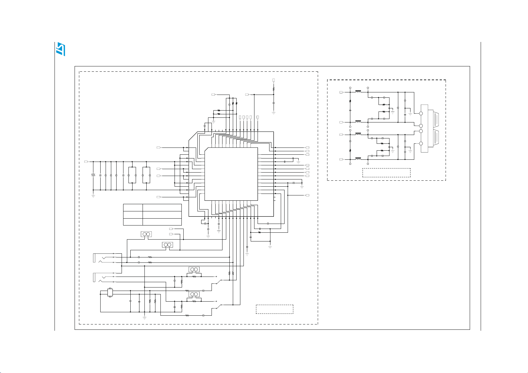
1.3 Schematic and block diagrams, bill of material, PCB layout
Figure 2. Schematic-1
+3V3
R5
10K
C4
1nF
SDI1
49
48
47
36
46
35
45
34
33
32
31
30
29
28
27
26
25
32
C9
1uF/10V
0ohm
C3
2u2/10V
44
43
42
41
40
39
38
37
36
35
34
33
C8
1uF/10V
STA381BWS
LRCKI
BICKI
MCLK
FFX4B
FFX4A
FFX3B
FFX3A
C5
100nF
+3V3
Doc ID 022081 Rev 3 7/65
+3V3
R3
0 ohm
R1
0 ohm
C11
100nF
63
64
606162
47
OUT2B
+VS
C428
470U/35V
+
C35
100nF
C33NSC14
1uF/50V
C429
C426A
C34
NS
NS
NS
OUT2A
100nF
100nF
1uF/50V
OUT1B
C427B
C427A
C426B
OUT1A
NOTE:
NS
C30
1uF/10V
C31
1uF/10V
C7
3.3nF/10V
CONFIGURATION
2.0CH & 2.1CH
MONO BT L
J15
1
2
J16
R6
11K
R7
11K
47K
47K
3.3nF/10V
R40
R39
F3XR
F3XL
1
HPJCKX3.5-06
Line in
J2
HPJCKX3.5-06
HEADER2X2
2
Line out
C56
100nF
J19
1
2
3
1
2
3
J7
1
34
C6
1
2
3
4
5
6
7
8
9
10
11
12
13
14
15
16
2
1
J14
R35
1K
C54
100nF
R46
470R
R37
1
J18
R44
1K
C55
100nF
R45
470R
R38
48
1
VDDDIG2
GNDDIG2
VCC_REG
TESTMODE
2
VSS_REG
3
OUT2B
4
GND2
5
VCC2
6
OUT2A
7
OUT1B
8
VCC1
9
GND1
10
OUT1A
11
VDD_REG
12
GND_REG
HALFVDD14F3XL15F3XR16HPIN_L17HPIN_R18LINEHPOUT_L19LINEHPOUT_R20GNDA21SOFTMUTE22VDD3V323CPVSS24CPM
13
171819202122232425262728293031
C1
1uF/10V
100nF
NS
C56
*
2
47R
2
47R
1
3
10uF/10V
C51
1
3
10uF/10V
C52
59
C53
2
SW2
2
SW3
58
44
45SA46
SCL
STA381BWS
STA381BWS_NEW
R8
27K
RESET
NS
NS
100nF
R4
R2
C2
SDA
SCL
INT_LINE
PWRDN
53
54
505152
555657
37
38
39
40
41
42
43
SDI
SDA
IC1
IC3
BICKI
LRCKI
PWDN
RESET
INTLINE
R9
27K
1uF/10V
SOFTMUTE
AGNDPLL
VREGFILT
GNDDIG1
VDDDIG1
VDD3V3CHP
GNDPSUB
C29
100nF
C10
MCLK
FFX4B
FFX4A
FFX3B
FFX3A
CPP
R36
OUT1A
R42
20(S)
C44
330P(S)
L1
SWPA6045S220MT
OUT1B
OUT2A
OUT2B
C45
330P(S)
R43
20(S)
SWPA6045S220MT
L2
SWPA6045S220MT
L4
C37
C32
NS
220nF
R10
0R
0R
R11
220nF
NS
C36
C38
NS
C41
C43
0R
220nF
R41
0R
R30
220nF
NS
C40
C42
C47
1N(S)
C46
220nF
220nF
4
C50
1N(S)
3
2
C48
1N(S)
1
C39
C49
1N(S)
SPEAKJA CK2X2
J9
L3
SWPA6045S220MT
OUTPUT FILTER
Note 1:
The output filter for the line/HP output
path is optional (not required for the STA381BW/S).
If the 2x 47 ohm resistors (R35 and R44) are
bypassed through J14 and J18, the 2x 100 nF
capacitors (C54 and C55) must also be removed.
Note 2:
C56 is not soldered when the STA 381BW/S
is configured in 2.0 or 2.1 channels; C56 is 100 nF
when the STA 381BW/S is configured in mono BTL.
Refer to the s
for an example of a mono BTL application.
chematic in Appendix A on page 63
AN3959 Functional description of the demonstration board
Page 8
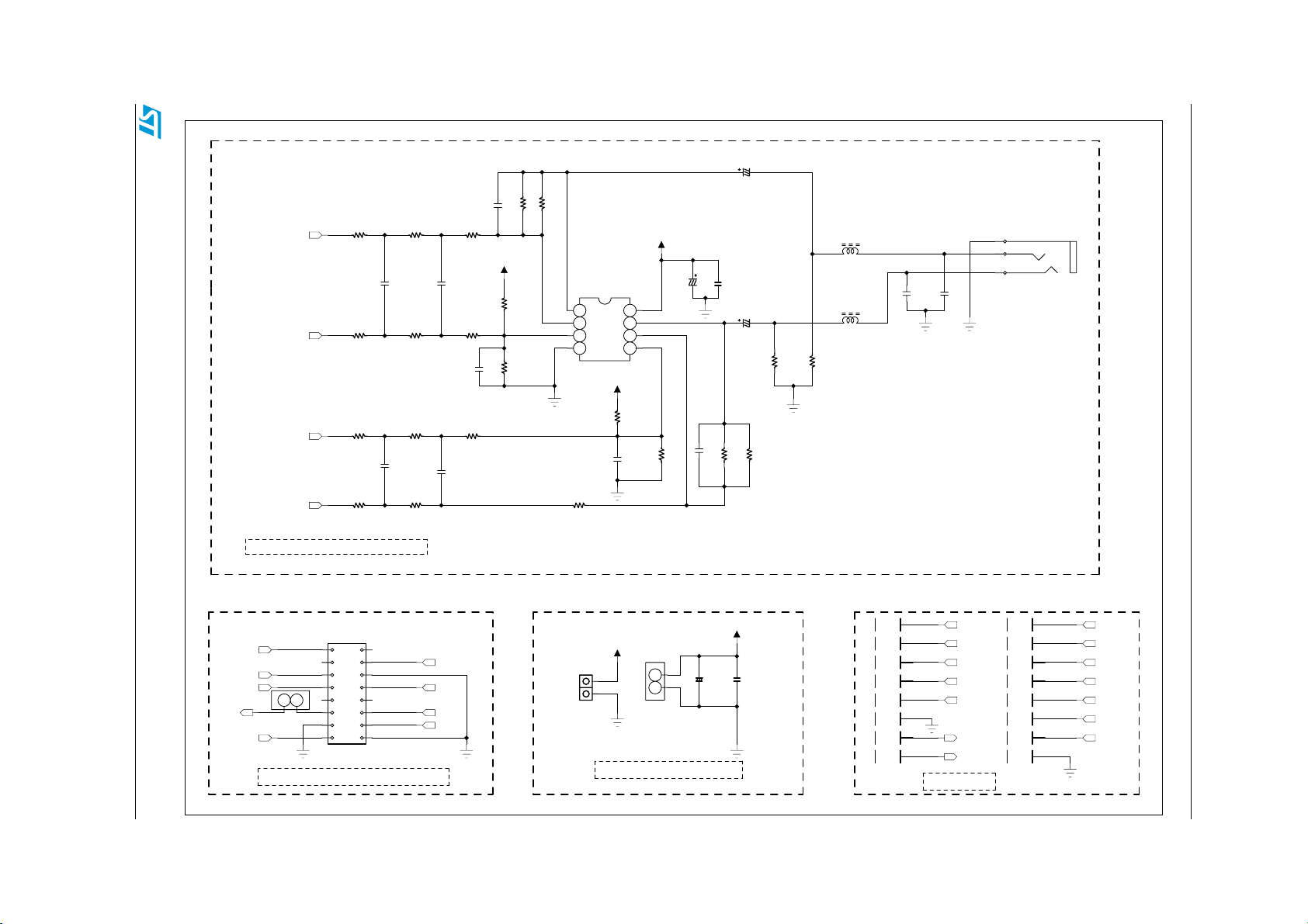
Figure 3. Schematic-2
Doc ID 022081 Rev 3 8/65
R12
FFX3B
FFX3A
FFX4B
FFX4A
4K7
C16
470PF
R13
4K7
R20
4K7
C19
470PF
R21
4K7
STEREO HEA DPHONE DRIVER
AN3959 Functional description of the demonstration board
C15
100uF
35V
10K
10K
C22
220PF
R29
R31
+VS
+VS
IC2
R27
4K7
LM833
1
2
3
4
OUTA
INA1
OUTB
INA2
VSS5INB2
VDD
INB1
+VS
R24
10K
220PF
C21
10K
R16
10K
R17
220PF
C28
47uF
8
7
6
10K
R25
C27
100nF
50V
C25
100uF
35V
10K
R34
220PF
C23
10K
10K
R33
R32
BD3
BEAD or 33R
C26
C24
100PF
100PF
BD4
BEAD o r 33R
10K
R28
1
2
3
HEADPHONE O/P
J13
C17
150PF
C20
150PF
R18
4K7
R19
4K7
C18
R26
4K7
R14
4K7
R15
4K7
R22
4K7
R23
4K7
+3V3
SDI1
BICKI
J17
MCLK
12
1
2
11 12
13 14
15 16
TO AP INTERFACE
AP INTERFACE CONNECTOR
J1
HEADER8X2
34
56
78
910
LRCKI
SDASCL
RESET
PWRDN
+VS
CN1
CN2
CN-5-02P
1
2
+
1
2
C12
10uF/10V
The r ange of +Vs is f rom +5V t o +24V
POWER SUPPLY INPUT
+3V3
C13
100nF
J3-1
J4-1
J3-2
J4-2
J6-1
J6-2
SDA
J5-1
SCL
J5-2
MCLK
LRCKI
BICKI
SDI1
INT_LINE
SDA
SCL
J8-1
J8-2
J10-1
J10-2
J11-1
J11-2
J12-1
J12-2
FFX3A
FFX3B
FFX4A
FFX4B
F3XL
F3XR
SOFTMUTE
TEST PINS
Page 9
AN3959 Functional description of the demonstration board
Table 1. Bill of material
No. Type Footprint Description Qty Reference Manufacturer
1 Jack Speaker jack MP4-16 1 J9 Songchen
Headphone
2
3Switch
4 Terminal Through-hole
5 Header Through-hole 4P (2x2 row) 2.54 mm header 1 J7 Any source
6 Header Through-hole 2P (2x1 row) 2.54 mm header 14
7 Header Through-hole 16P (8x2 row) 2.54 mm header 1 J1 Any source
8 CCAP CAP0603 50 Volt NPO 100 pF +/-10% 2 C24, C26 Murata
9 CCAP CAP0603 50 Volt NPO 150 pF +/-10% 2 C17, C20 Murata
10 CCAP CAP0603 50 Volt NPO 220 pF +/-10% 4 C18, C21, C22, C23 Murata
11 CCAP CAP0603 50 Volt NPO 330 pF +/-10% 2 C44, C45 Murata
12 CCAP CAP0603 50 Volt NPO 470 pF +/-10% 2 C16, C19 Murata
13 CCAP CAP0603 50 Volt 1 nF +/-10% 5 C4, C47, C48, C49, C50 Murata
14 CCAP CAP0603 50 Volt 3.3 nF +/-10% 2 C6, C7 Murata
15 CCAP CAP0603 50 Volt 100 nF +/-10% 12
16 CCAP CAP0603 50 Volt 220 nF +/-10% 4 C32, C36, C42, C43 Murata
17 CCAP CAP0603 NS 5 C37, C38, C40, C41, C56 Murata
jack
Phone jack
Deviator
switch
SONGCHEN CKX-3.5-06
3-pin
Deviator switch 2 SW2, SW3 Any source
2P pitch: 5mm connector
terminal
3 J2, J13, J19 Songchen
1 CN2
J3, J4, J5, J6, J8, J10,
J11, J12, J14, J15, J16,
J17, CN1, J18
C1, C2, C5, C11, C13,
C27, C29, C54, C55,
C429, C427A, C427B
Phoenix
Contact
Any source
Murata
18 CCAP CAP0805 10 Volt 1 µF +/-10% 5
19 CCAP CAP0805 10 Volt 2.2U +/-10% 1 C3 Murata
20 CCAP CAP1206 50 Volt 220 nF +/-10% 2 C39, C46 Murata
21 CCAP CAP1206 50 Volt 1U +/-10% 2 C426A, C426B Murata
22 CCAP CAP1206 10 Volt 10 µF +/-10% 2 C51, C52 Murata
23 CCAP CAP1206 NS 4 C14, C33, C34, C35 Murata
24 ECAP CAP1206 10µF/10V 1 C12 Samsung
25 ECAP Through-hole 47µF/35V 105 Centigrade 1 C28
26 ECAP Through-hole 100µF/35V 105 Centigrade 2 C15, C25
27 ECAP Through-hole
470µF/25V, pitch = 5 mm,
φ 10 mm
Doc ID 022081 Rev 3 9/65
C8, C9, C10, C30,
C31, C53
1C428
Murata
Rubycon/
Panasonic
Rubycon/
Panasonic
Rubycon/
Panasonic
Page 10
Functional description of the demonstration board AN3959
Table 1. Bill of material (continued)
No. Type Footprint Description Qty Reference Manufacturer
28 RES R1206 0R 4 R10, R11, R30, R41 Murata
29 RES R1206 20 +/-5% 1/8W 2 R42, R43 Murata
30 RES R0603 0 ohm 1/16W R1, R3, R36 Murata
31 RES R0603 47R +/-5% 1/16W 2 R35, R44 Murata
32 RES R0603 470R +/-5% 1/16W 2 R37, R38 Murata
33 RES R0603 1K +/-5% 1/16W 2 R45, R46 Murata
R5, R16, R17, R24, R25,
34 RES R0603 10K +/-5% 1/16W 11
35 RES R0603 11K +/-5% 1/16W 2 R6, R7 Murata
36 RES R0603 4.7K +/-5% 1/16W 12
37 RES R0603 47K +/-5% 1/16W 2 R39, R40 Murata
38 RES R0603 NS R2, R4 Murata
R28, R29, R31, R32,
R33, R34
R12, R13, R14, R15,
R18, R19, R20, R21,
R22, R23, R26, R27
Murata
Murata
39 RES R0805 27K +/-5% 1/16W 2 R8, R9 Murata
40 Bead L0805
41 Plastic rod
42 Plastic rod
43 IC
44 IC SOP8 LM833D (SOP8) 1 IC2 ST
45 Coil SMD SWPA6045S220MT, 22 µH 4 L1, L2, L3, L4 Sunlord
46 PCB STA381BWS 2.0CH REV2.2 1 Fastprint
QFN48 or
QFP64
Bead 600 ohm at 100 MHz or
33R
Hexagonal rod 15 mm length,
male type
Hexagonal rod 8 mm length,
female type
STA381BWS (QFN48 or
QFP64)
2BD3, BD4 Murata
4 Four corners Any source
4 Four corners Any source
1 IC1 or IC3 ST
10/65 Doc ID 022081 Rev 3
Page 11
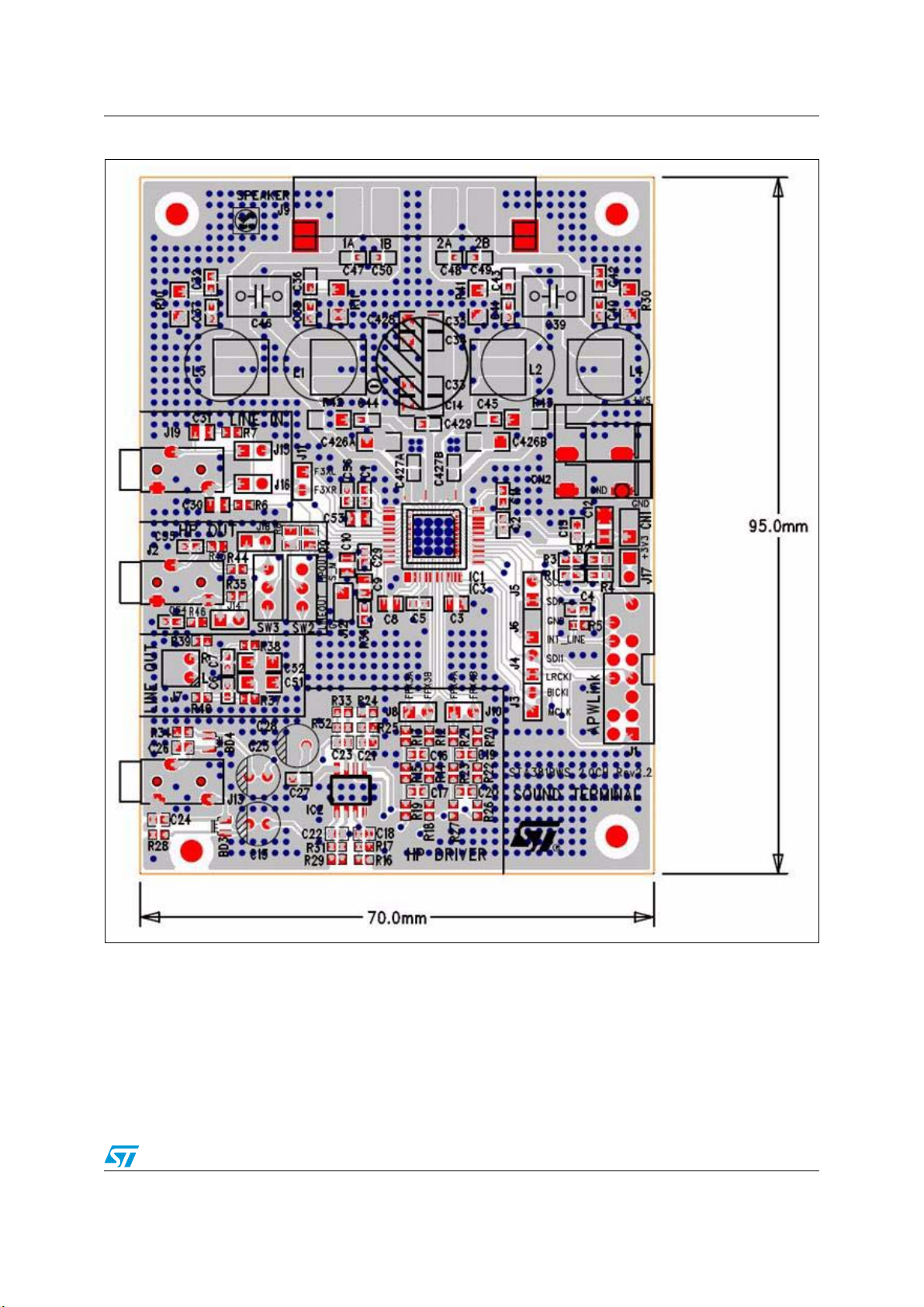
AN3959 Functional description of the demonstration board
Figure 4. Top view of PCB layout
Doc ID 022081 Rev 3 11/65
Page 12
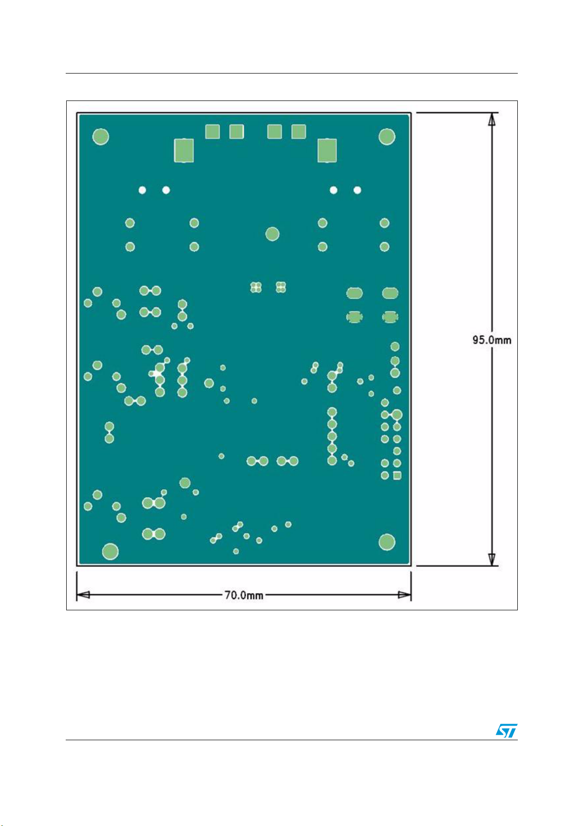
Functional description of the demonstration board AN3959
Figure 5. Inner layer2 view of PCB layout
12/65 Doc ID 022081 Rev 3
Page 13
AN3959 Functional description of the demonstration board
Figure 6. Inner layer3 view of PCB layout
Doc ID 022081 Rev 3 13/65
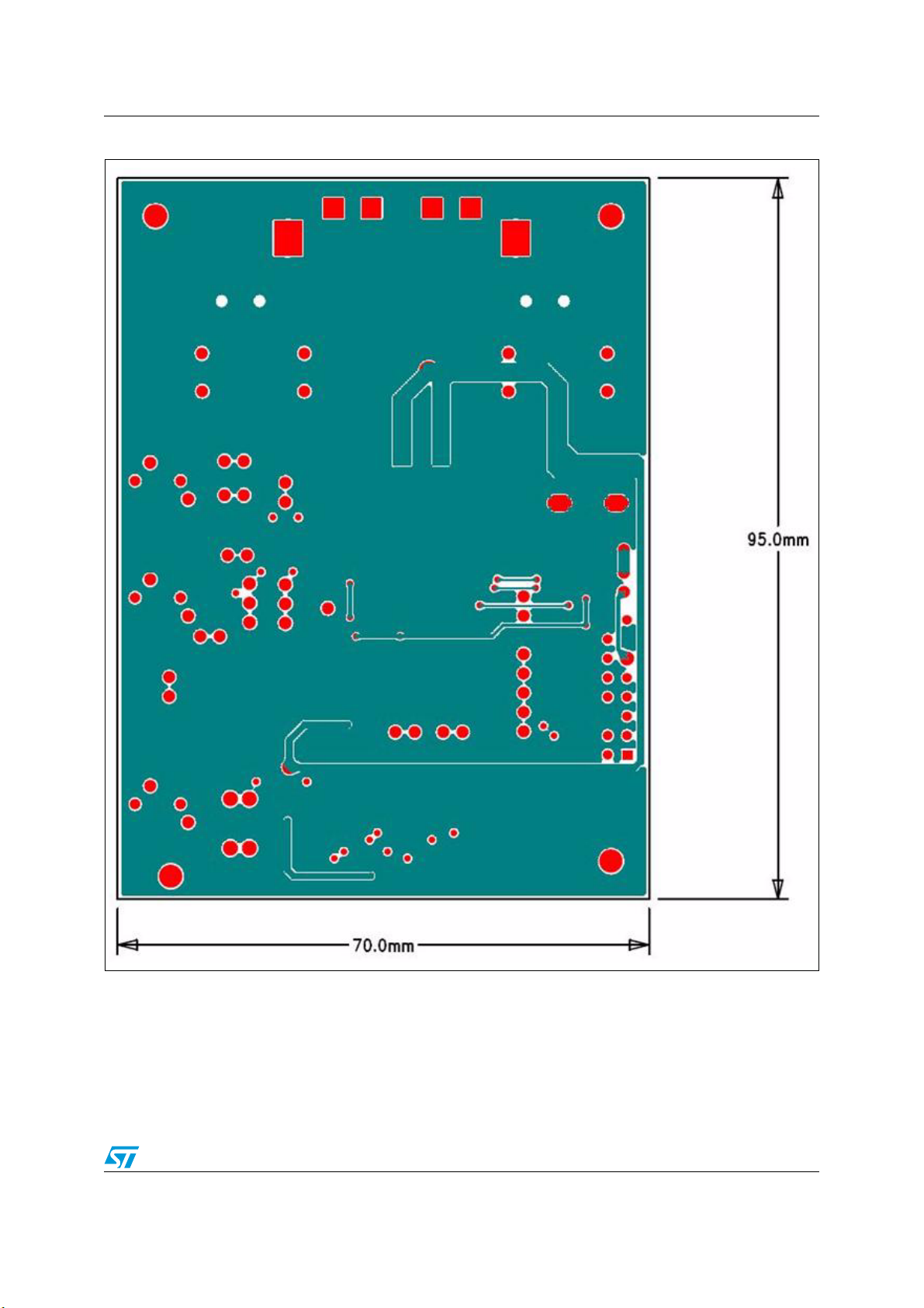
Page 14
Functional description of the demonstration board AN3959
Figure 7. Bottom view of PCB layout
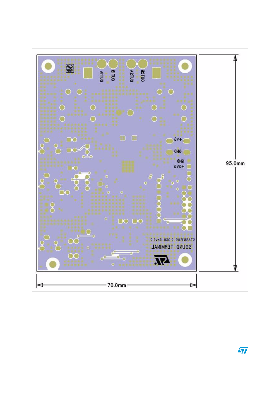
14/65 Doc ID 022081 Rev 3
Page 15
AN3959 Functional description of the demonstration board
g
(
(
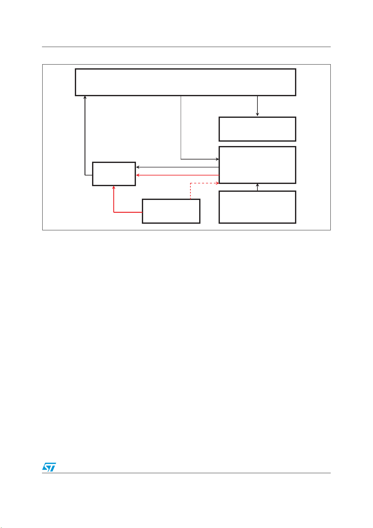
Figure 8. Block diagram of test connections with equipment
Output
to AP
STA380BWS
2.0CH
Demo
Board
From 4.5V to24V
Audio Precision Equipment
S/PDIF
nal
Si
I2S Input
DC3V3)
DC7V)
DC Power Supply
Monitor
Digital Oscilloscope
TDS3034B Tektronix
APWLink Board
PC with GUI to control the
chipset
Doc ID 022081 Rev 3 15/65
Page 16
STA381BWS power section test results AN3959
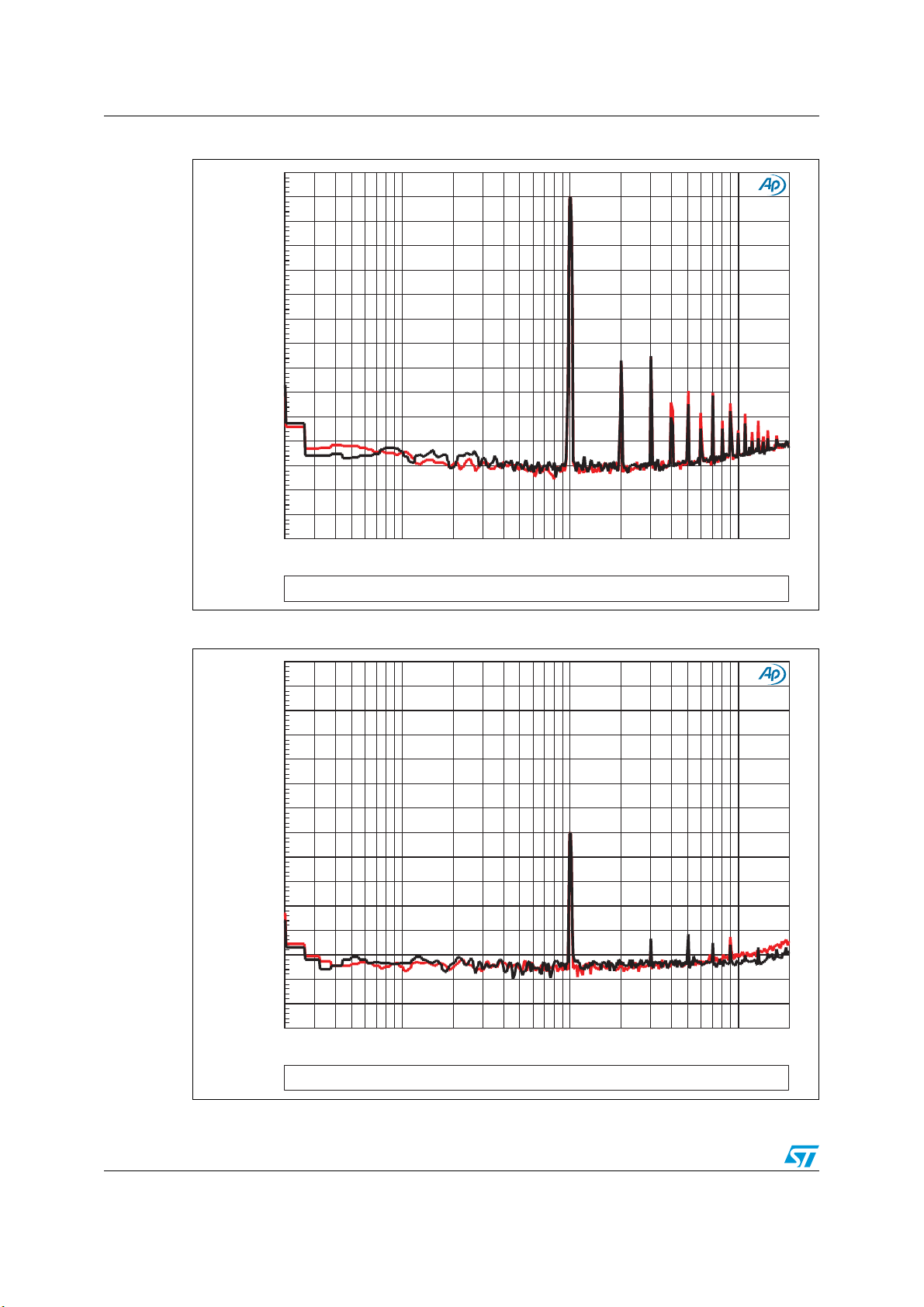
2 STA381BWS power section test results
Figure 9. Frequency response, VCC = 18 V, RL = 8 ohm, 0 dB (Pout = 1 W)
+3
+2.5
+2
+1.5
+1
+0.5
d
B
+0
r
A
-0.5
-1
-1.5
-2
-2.5
-3
20 20k50 100 200 500 1k 2k 5k 10k
Test Conditions: VCC=18V, Rl=8ohm, Dual BTL, Input Signal=-14dBFS, Pout=1W, Volum e: +3dB
Figure 10. Crosstalk, V
+0
-10
-20
-30
-40
d
B
r
-50
A
-60
-70
-80
-90
Hz
= 18 V, RL = 8 ohm, 0 dB (Pout = 1 W)
CC
-100
20 20k50 100 200 500 1k 2k 5k 10k
Test Conditions: VCC=18V, Rl=8ohm, Dual BTL, Pout=1W, Volum e: +3dB
16/65 Doc ID 022081 Rev 3
Hz
Page 17
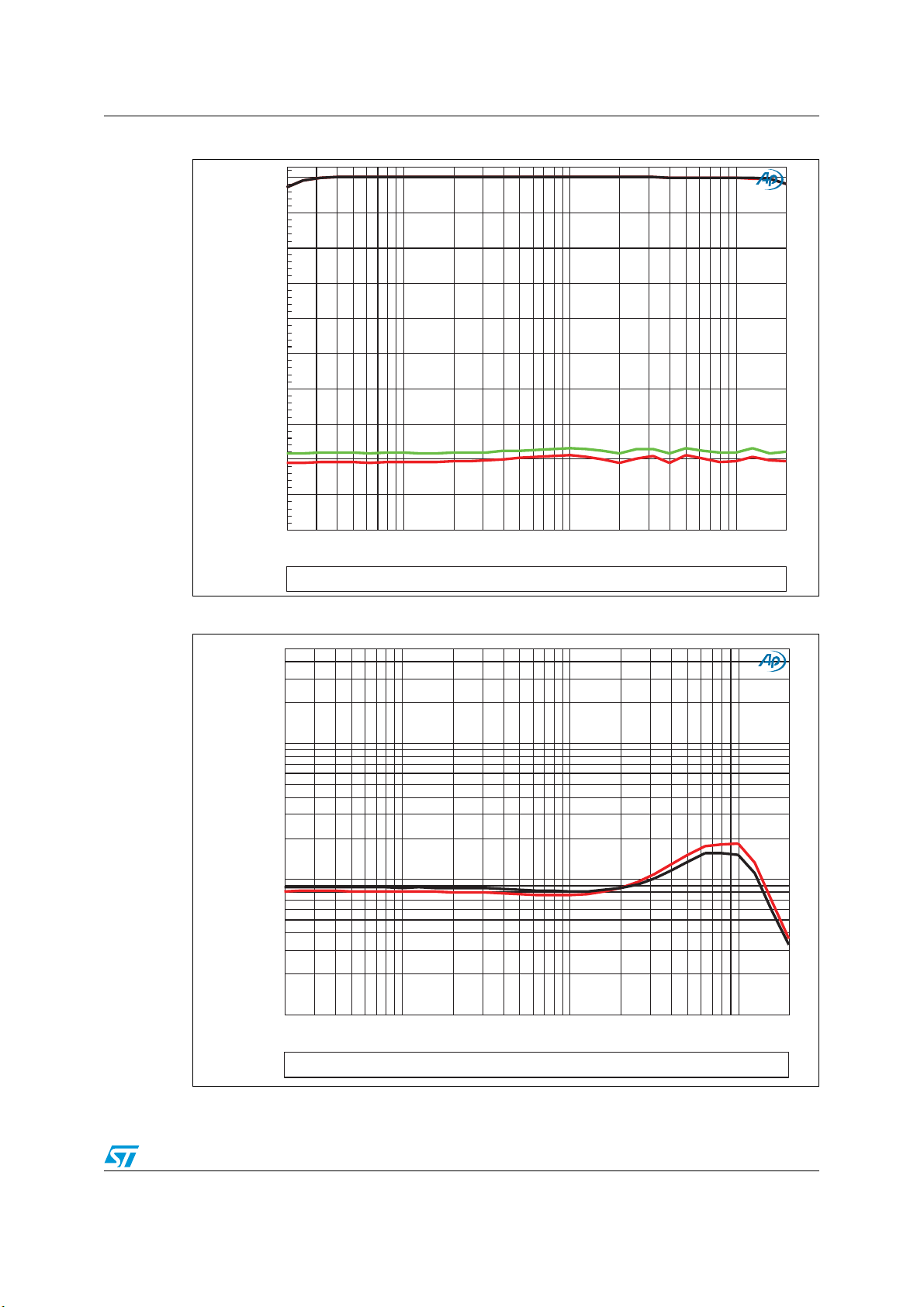
AN3959 STA381BWS power section test results
Figure 11. SNR, VCC = 18 V, RL = 8 ohm, 0 dB (Pout = 1 W)
+0
-10
-20
-30
-40
d
B
r
-50
A
-60
-70
-80
-90
-100
20 20k50 100 200 500 1k 2k 5k 10k
Hz
Test Conditions: VCC=18V, Rl=8ohm, Dual BTL, Pout=1W, Volume: +3dB
Figure 12. THD vs. frequency, V
5
2
1
0.5
%
0.2
0.1
0.05
0.02
0.01
20 20k50 100 200 500 1k 2k 5k 10k
Test Conditions: VCC=18V, Rl=8ohm, Dual BTL, Pout=1W, Volum e: +3dB
= 18 V, RL = 8 ohm, Pout = 1 W
CC
Hz
Doc ID 022081 Rev 3 17/65
Page 18
STA381BWS power section test results AN3959
Figure 13. FFT (0 dBFS), VCC = 18 V, RL = 8 ohm, 0 dBFS (Pout = 1 W)
+10
+0
-10
-20
-30
-40
-50
d
B
-60
r
-70
A
-80
-90
-100
-110
-120
-130
-140
20 20k50 100 200 500 1k 2k 5k 10k
Hz
Test Conditions: VCC=18V, Rl=8ohm, f=1KHz, Dual BTL, Input Signal=0dBFS, Pout=1W, Volum e: -11.5dB
Figure 14. FFT (-60 dBFS), V
+10
+0
-10
-20
-30
-40
-50
d
B
-60
r
-70
A
-80
-90
-100
-110
-120
-130
-140
20 20k50 100 200 500 1k 2k 5k 10k
Test Conditions: VCC=18V, Rl=8ohm, f=1KHz, Dual BTL, Input Signal=-60dBFS, Volume: -11.5dB
= 18 V, RL = 8 ohm, 0 dBFS (Pout = 1 W)
CC
Hz
18/65 Doc ID 022081 Rev 3
Page 19
AN3959 STA381BWS power section test results
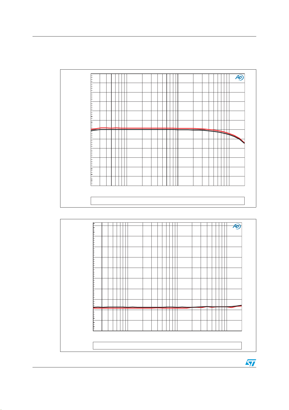
Figure 15. THD vs. output power, VCC = 18 V, RL = 8 ohm, f = 1 kHz
10
5
2
1
0.5
%
0.2
0.1
0.05
0.02
0.01
10m 2020m 50m 100m 200m 500m 1 2 5 10
W
Test Conditions: VCC=18V, Rl=8ohm, Dual BTL, Volum e: +3dB
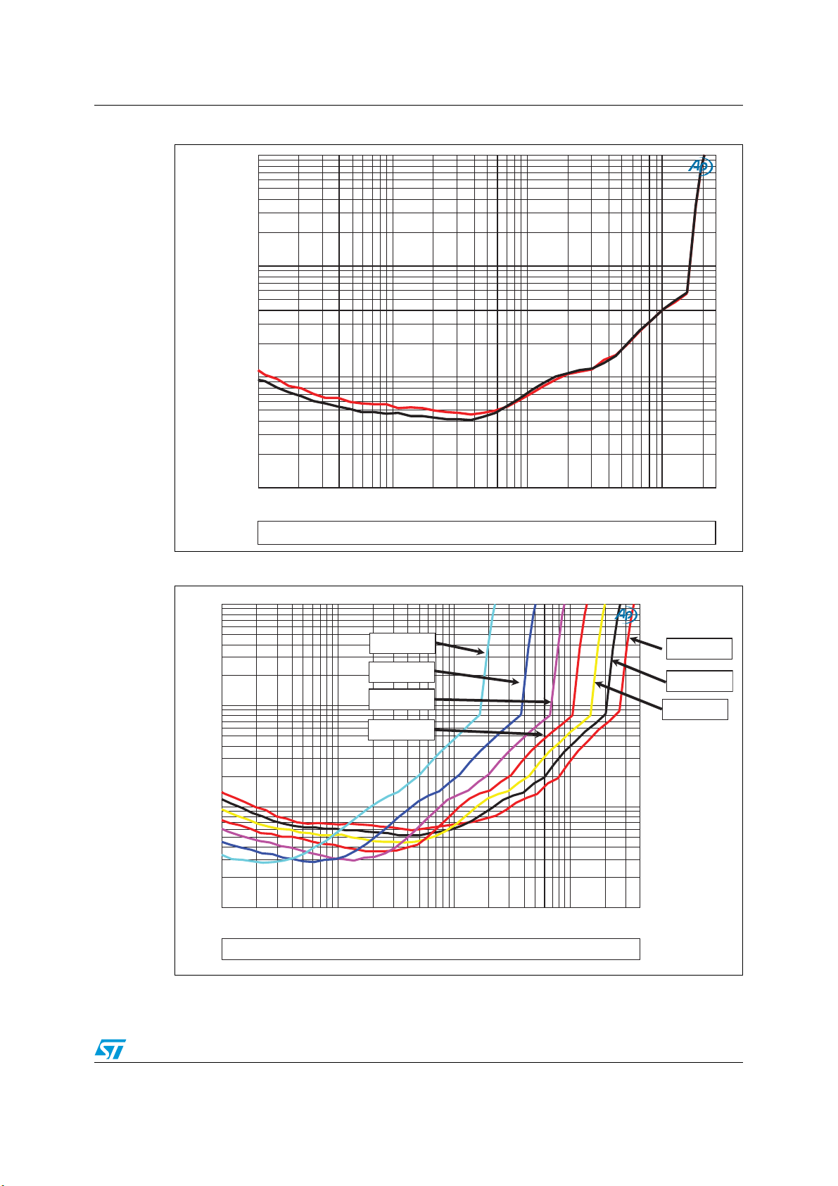
Figure 16. THD vs. output power at different power supplies, R
10
5
2
1
0.5
%
0.2
0.1
0.05
0.02
0.01
10m 4020m 50m 100m 200m 500m 1 2 5 10 20
Test Conditions: Rl=8ohm, Dual BTL, Volum e: +3dB
VCC=6V
VCC=9V
VCC=12V
VCC=15V
W
= 8 ohm, f = 1 kHz
L
VCC=24V
VCC=21V
VCC=18V
Doc ID 022081 Rev 3 19/65
Page 20
STA381BW power section test results AN3959
3 STA381BW power section test results
Figure 17. Frequency response, VCC = 24 V, RL = 8 ohm, 0 dB (Pout = 1 W)
+3
+2.5
+2
+1.5
+1
+0.5
d
B
+0
r
A
-0.5
-1
-1.5
-2
-2.5
-3
20 20k50 100 200 500 1k 2k 5k 10k
Test Conditions: VCC=24V, Rl=8ohm, Dual BTL, Input Signal=-17dBFS, Pout=1W, Volume: +3dB
Figure 18. Crosstalk, V
+0
-10
-20
-30
-40
d
B
r
-50
A
-60
-70
-80
Hz
= 24 V, RL = 8 ohm, 0 dB (Pout = 1 W)
CC
-90
-100
20 20k50 100 200 500 1k 2k 5k 10k
Test Conditions: VCC=24V, Rl=8ohm, Dual BTL, Pout=1W, Volum e: +3dB
20/65 Doc ID 022081 Rev 3
Hz
Page 21

AN3959 STA381BW power section test results
Figure 19. SNR, VCC = 24 V, RL = 8 ohm, 0 dB (Pout = 1 W)
+0
-10
-20
-30
-40
d
B
r
-50
A
-60
-70
-80
-90
-100
20 20k50 100 200 500 1k 2k 5k 10k
Hz
Test Conditions: VCC=24V, Rl=8ohm, Dual BTL, Pout=1W, Volum e: +3dB
Figure 20. THD vs. frequency, V
5
2
1
0.5
%
0.2
0.1
0.05
0.02
0.01
20 20k50 100 200 500 1k 2k 5k 10k
Test Conditions: VCC=24V, Rl=8ohm, Dual BTL, Pout=1W, Volum e: +3dB
= 24 V, RL = 8 ohm, Pout = 1 W
CC
Hz
Doc ID 022081 Rev 3 21/65
Page 22

STA381BW power section test results AN3959
Figure 21. FFT (0 dBFS), VCC = 24 V, RL = 8 ohm, 0 dBFS (Pout = 1 W)
+10
+0
-10
-20
-30
-40
-50
d
B
-60
r
-70
A
-80
-90
-100
-110
-120
-130
-140
20 20k50 100 200 500 1k 2k 5k 10k
Hz
Test Conditions: VCC=24V, Rl=8ohm, f=1KHz, Dual BTL, Input Signal=0dBFS, Pout=1W, Volume: -13.5dB
Figure 22. FFT (-60 dBFS), V
+10
+0
-10
-20
-30
-40
-50
d
B
-60
r
-70
A
-80
-90
-100
-110
-120
-130
-140
20 20k50 100 200 500 1k 2k 5k 10k
Test Conditions: VCC=24V, Rl=8ohm, f=1KHz, Dual BTL, Input Signal=0dBFS, Pout=1W, Volume: -13.5dB
= 24 V, RL = 8 ohm, 0 dBFS (Pout = 1 W)
CC
Hz
22/65 Doc ID 022081 Rev 3
Page 23

AN3959 STA381BW power section test results
Figure 23. THD vs. output power, VCC = 24 V, RL = 8 ohm, f = 1 kHz
10
5
2
1
0.5
%
0.2
0.1
0.05
0.02
0.01
10m 4020m 50m 100m 200m 500m 1 2 5 10 20
W
Test Conditions: VCC=24V, Rl=8ohm, Dual BTL, Volume: +3dB
Figure 24. THD vs. output power at different power supplies, R
10
5
2
1
0.5
%
0.2
0.1
0.05
0.02
0.01
60m 50100m 200m 500m 1 2 5 10 20
Test Conditions: Rl=8ohm, Dual BTL, Volum e: +3dB
VCC=6V
VCC=9V
VCC=12V
VCC=15V
W
= 8 ohm, f = 1 kHz
L
VCC=27V
VCC=24V
VCC=21V
VCC=18V
Doc ID 022081 Rev 3 23/65
Page 24

Analog section test results AN3959
4 Analog section test results
The line/headphone out can be fed either with an external analog source, or with the F3X
output, allowing the audio content to come from the digital interface on both the power
output and on the line/headphone out.
Table 2. Test conditions
Conditions Input Output
J15, J16 short-circuit & SW2, SW3 switch to HPOUT STA381BWS F3X F3X HP OUT
J15, J16 short-circuit & SW2, SW3 switch to LINEOUT STA381BWS F3X LINE OUT
J15, J16 open circuit & SW2, SW3 switch to HPOUT LINE IN F3X HP OUT
J15, J16 open circuit & SW2, SW3 switch to LINEOUT LINE IN LINE OUT
Table 3. Headphone section test results
Filter: 22K LPF Ext. Res: 18K + 43K
Headphone Unit Spec. Test results
Reference mVrms 75 mVrms reference
Maximum output level
Left
Right
H/P frequency response
Right
H/P THD+N vs. frequency
Left
Right
H/P THD+N vs. level
Left
Right
H/P signal-to-noise (20-bit)
Left
Right
mVrms 540 mVrms(10 mW) 542 mV
-3 dB↑, +0.5 dB 30 Hz
~20 kHz
dBr -57 77
dBr -57 77
dBr -60
548 mV
-0.4 ~ -0.28Left
77
77
78
78
24/65 Doc ID 022081 Rev 3
Page 25

AN3959 Analog section test results
Table 4. Line out section test results
Filter: 22K LPF Ext Res: 18K + 43K
Line out Unit Spec. Test results
Reference 200 mV +/-20%
Maximum output level
Left
Right
Frequency response
Left
Right
THD+N vs. frequency
Left
Right
TH+N vs. level
Left
Right
Signal-to-noise (20-bit)
Left
Right
Channel separation
Left
Right
L/R CH phase difference deg 5↓ 0.02
Dynamic range (20-bit)
mVrms 2.0 V↓ 1.86
1.87
-1 dB↑,+0.5dB↓ 20Hz
~20 kHz
dBr -60
dBr -60 -78 dB at 200 mV
dBr -70 79
dBr -70 99
-0.87 dB at 20 Hz
-0.83 dB at 20 Hz
-71 dB at 20 Hz
-71 dB at 20 Hz
-78 dB at 200 mV
79
80
Left
Right
Residual noise mV 7↓ 0.021 mV
dBr -85 100
100
Doc ID 022081 Rev 3 25/65
Page 26

Thermal performance AN3959
5 Thermal performance
5.1 Thermal results - test 1
Figure 25. Temperature test 1
Testing conditions:
● V
● 1 kHz sine wave
● 8 ohm
= 12 V
CC
Output power: 2 x 7 W
Table 5. Thermal results - test 1
Result Tamb = 25 °C Tamb = 40°C
IC temp 39.2 °C 54.2 °C
26/65 Doc ID 022081 Rev 3
Page 27

AN3959 Thermal performance
5.2 Thermal results - test 2
Figure 26. Temperature test 2
Testing conditions:
● V
● 1 kHz sine wave
● 8 ohm
= 24 V
CC
Output power: 2 x 15 W
Table 6. Thermal results - test 2
Result Tamb = 25 °C Tamb = 40°C
IC temp 74.5 °C 89.5 °C
Doc ID 022081 Rev 3 27/65
Page 28

Design guidelines for schematic and PCB layout AN3959
6 Design guidelines for schematic and PCB layout
6.1 Schematic
6.1.1 Criteria for selection of components
● Absolute maximum rating: STA381BWS V
● Bypass capacitor 100 nF in parallel to 1 µF for each power V
dielectric is X7R.
● Coil saturation current compatible with the peak current of application
6.1.2 Decoupling capacitors
For the decoupling capacitor(s), one decoupling system can be used with 2 capacitors per
channel. The decoupling capacitors must be as close as possible to the IC pins, in order to
avoid parasitic inductance with the copper wire on the PC board.
6.1.3 Output filter
Figure 27. Output filter (BTL)
IN xA
C90
330p
R36
20
IN xB
22u
L11
L13 22u
C89
100n
C95
100n
C101
100n
C105
100n
= 27 V
CC
R34
6.2
R37
6.2
C98
470n
branch. Preferable
CC
C91
1000p
C99
1000p
C103
1000p
J7
1
2
CON2
SNUBBER
Main Filter
1. The key function of a snubber network is to absorb energy from the reactance in the
power circuit. The purpose of the snubber RC network is to avoid unnecessary high
pulse energy such as a spike in the power circuit which is dangerous to the system.
The snubber network allows the energy (big spike) to be transferred to and from the
snubber network in order for the system to work safely.
2. The purpose of the main filter is to cut off the frequency above the audible range of
20 kHz, which is mandatory in order to have a clean amplifer response. The main filter
is designed using the Butterworth formula to define the cutoff frequency.
3. The purpose of the damping network is to avoid the high-frequency oscillation issue on
the output circuit. The damping network allows the THD to be improved and also allows
avoiding the inductive copper on the PCB route when the system is working at high
frequency with PWM or PCM.
28/65 Doc ID 022081 Rev 3
Dumping Network
Page 29

AN3959 Design guidelines for schematic and PCB layout
6.1.4 Snubber filter
The snubber circuit must be optimized for the specific application. Starting values are
330 pF in series to 22 ohm. The power on this network is dependent on the power supply,
frequency and capacitor value according to the following formula:
P=C*f*(2*V)
2
This power is dissipated on the series resistance.
Figure 28. Differential-mode snubber circuit
INxA
C126
330p
R44
22
INxB
For the common-mode snubber the formula to evaluate power is:
P=C*f*2*(V
2
)
This power is dissipated on the series resistance.
Figure 29. Common-mode snubber circuit
INxA
C127
330p
R45
22
R46
22
C130
INxB
330p
Doc ID 022081 Rev 3 29/65
Page 30

Design guidelines for schematic and PCB layout AN3959
6.1.5 Main filter
The main filter is an L and C based Butterworth filter. The cutoff frequency must be chosen
between the upper limit of the audio band (≈20 kHz) and the carrier frequency (384 kHz).
Figure 30. Main filter
6.1.6 Dumping network
The C-R-C is a dumping network. It is mainly intended for high inductive loads such as
disconnecting the speaker load.
Figure 31. Dumping network
C dump -S
C dump -P
C dump -P
C dump -S
Table 7. Recommended values
Rload 16 ohm 12 ohm 8 ohm 6 ohm 4 ohm
Lload 47 µH 33 µH 22 µH 15 µH 10 µH
Cload 220 nF 330 nF 470 nF 680 nF 1 µF
R dump
Rdump
C dump-S 100 nF 100 nF 100 nF 100 nF 220 nF
C dump-P 100 nF 100 nF 100 nF 100 nF 220 nF
R dump 10 8.2 6.2 4.7 2.7
30/65 Doc ID 022081 Rev 3
Page 31

AN3959 Design guidelines for schematic and PCB layout
6.1.7 Recommended power-up and power-down sequence
There is no constraint regarding power supply voltages while it is required to release the
reset line (RST) only after the master clock (MCLK) is stable, after the power-down (PWDN)
is already set high and before any I
Figure 32. Recommended power-up and power-down sequence
2
C commands.
6.2 Layout
The following figures illustrate layout recommendations.
Figure 33. Snubber network soldered as close as possible to the respective IC pin
Doc ID 022081 Rev 3 31/65
Page 32

Design guidelines for schematic and PCB layout AN3959
Figure 34. Electrolytic capacitor used first to separate the VCC branches
Figure 35. Path between V
and ground pin minimized in order to avoid inductive paths
CC
32/65 Doc ID 022081 Rev 3
Page 33
AN3959 Design guidelines for schematic and PCB layout
Thermal dissipation
It is mandatory to have a large ground plane on the top layer, inner layer2, inner layer3, and
bottom layer and solder the slug on the PCB.
Figure 36. Large ground plane on the top side
Figure 37. Large ground plane on inner layer2
Doc ID 022081 Rev 3 33/65
Page 34

Design guidelines for schematic and PCB layout AN3959
Figure 38. Large ground plane on inner layer3
34/65 Doc ID 022081 Rev 3
Page 35

AN3959 Design guidelines for schematic and PCB layout
Figure 39. Large ground plane on bottom side
Figure 40. Symmetrical paths created for output stage, for differential applications
Doc ID 022081 Rev 3 35/65
Page 36
Design guidelines for schematic and PCB layout AN3959
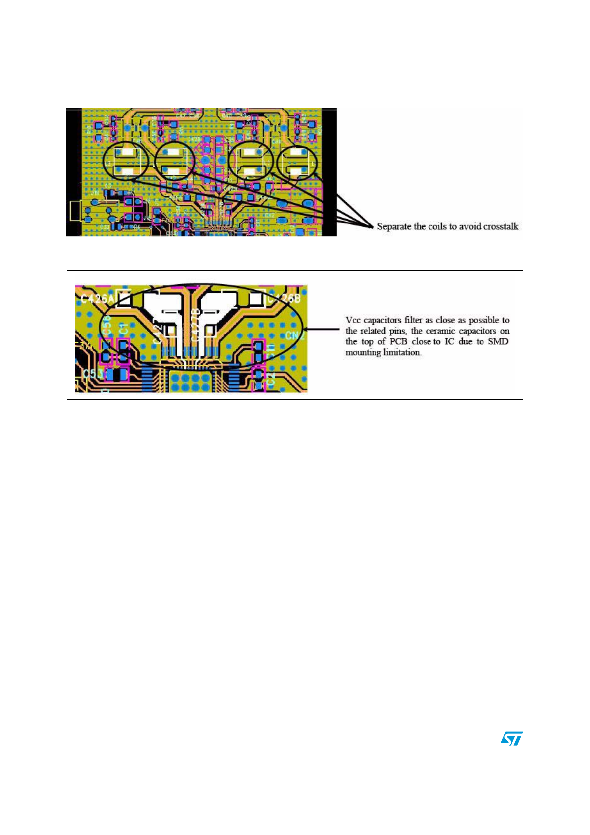
Figure 41. Coils separated in order to avoid crosstalk
Figure 42. V
filter for high frequency
CC
Placing the V
filter capacitors close to the pins avoids an inductive coil generated by the
CC
copper wire, because the system is working in PWM with fast switching (the frequency is
384 kHz with fs = 48 kHz) so the longer copper wire easily becomes an inductor. To improve
this we suggest using the ceramic capacitor to balance the reactance. It's mandatory to put
the ceramic capacitor as close as possible to the related pins. The distance between the
capacitor to the related pins is recommended to be within 5 mm.
36/65 Doc ID 022081 Rev 3
Page 37

AN3959 Design guidelines for schematic and PCB layout
Figure 43. Thermal layout with large ground
The thermal resistance junction in the bottom of the STA381BWS to ambient, obtainable
with a ground copper area of 5.6 x 5.6 mm and with 16 via holes is shown in Figure 43 as an
example.
Doc ID 022081 Rev 3 37/65
Page 38

Software setup to use the STA381BW/STA381BWS devices (ST Map) AN3959
7 Software setup to use the STA381BW/STA381BWS
devices (ST Map)
7.1 Processing configuration
Figure 44. Processing path
Proc essing Frequency = 2xFs
I2S In p ut
Interface
X2Ov er-
-sampling
FIR
X2Ov er-
-sampling
FIR
Proc essing Frequency = 2xFs
Pre-
-scale
Pre-
-scale
Hi-Pass
Filter
By de fault tw o ch an nels
Hi-Pass
Filter
Biquad#1Biquad#2Biquad#3Biquad
are link ed
Biquad#1Biquad#2Biquad#3Biquad
● By default, the post-scale is linked (all channels use the channel-1 coefficient value)
– To use different coefficients, bit D3 register 0x03 must be set to 0
● By default, all 8 biquads are enabled
● By default, all biquads are linked (all channels use the channel-1 coefficient values)
– To use different coefficients, bit D4 register 0x03 must be set to 0
● By default, bass and treble are bypassed
– To use bass, bit D1 register 0x36 must be set to 0
– To use treble, bit D0 register 0x36 must be set to 0
Figure 45. 2.1-channel with STCompressor
L
C1Mx1
+
R
C1Mx2
Channel ½
Biquad #8
--------------
Hi-pass XO
Filter
User D efined Filters
User D efined Filters
TM
STCompressor
#4
#4
Volum e
And
Limiter
Biquad #5
De-emph
By d efault two c han nels
Biquad #5
Or
De-emph
Or
are link ed
Biquad #6
Bass
Biquad #6
Bass
DC Cut
Filter
Or
Tone Control
Or
Tone Control
By d efault the ch annels
Biquad #7
or
Treble
Biquad #7
or
Treble
are link ed
Pos t Scale
L
R
C2Mx1
+
C2Mx2
C3Mx1
+
C3Mx2
User-Defined
Mix Coefficients
Channel ½
Biquad #8
--------------
Hi-pass XO
Filter
Channel 3
Biquad #8
--------------
Low -pass XO
filte r
Crossov er Frequency
Determ ined by XO Setting
(User D efined If
XO=0000)
STCompressor
38/65 Doc ID 022081 Rev 3
Volum e
And
Limiter
Volum e
And
Limiter
DC Cut
Filter
DC Cut
Filter
Pos t Scale
Pos t Scale
Page 39

AN3959 Software setup to use the STA381BW/STA381BWS devices (ST Map)
7.2 STCompressor
TM
Figure 46. STCompressor - overview
BQ0 BQ1
Input
Ch0
BQ0
BQ1
Band Splitter
BQ2 BQ3
Input
Ch1
BQ2
BQ3
Band Splitter
Level
Meter
Level
Meter
Level
Meter
Level
Meter
DRC0
Mapper
Mapper
DRC1
DRC2
Mapper
Mapper
DRC3
Offset
Attenuator
Attenuator
Offset
Offset
Attenuator
Attenuator
Offset
X
Output
Ch0
+
X
X
Output
Ch1
+
X
Figure 47. STCompressor - mapper
● Linear zone
– Standard operation, input and output are linked to volume
● Compression zone
– The signal is compressed with a programmable ratio
● Compression ratio
– The ratio changes the compression slope
● Limiting zone
– The signal is limited to avoid unpredictable effects or damages
Doc ID 022081 Rev 3 39/65
Page 40

Software setup to use the STA381BW/STA381BWS devices (ST Map) AN3959
Figure 48. STCompressor - compression ratio
● The compression ratio is user-programmable
● By default the rate is 1:1 (no variable ratio)
● There are 16 different settings (from 0 to 15) and the ratio varies from 1:1 to 1:16
Figure 49. STCompressor - limiter threshold
● The limiter threshold is user-programmable
● By default the threshold is set to 0 dB
● There are 144 different settings (from -24 to +12 dB) with 0.25 dB/step
40/65 Doc ID 022081 Rev 3
Page 41

AN3959 Software setup to use the STA381BW/STA381BWS devices (ST Map)
Figure 50. STCompressor - offset control
● The offset is a user-programmable gain or volume control
● When the STC is used, it is better to use offset instead of volume for location in the
processing path
There are 192 different settings (from 0 to +48) with 0.25 dB/step
7.2.1 STCompressor settings
● By default the STCompressor is enabled and in pass-through
– Bit D4 of register 0x5A (STC_EN) is set to 1. This means STC is enabled
– Bit D5 of register 0x5A (STC_BYP) is set to 1. This means STC is in pass-through
● By default the STC band recombination is disabled
– Bit D0 register 0x5B (BRC_EN) is set to 0
7.2.2 Configuring and enabling the STCompressor
● Write the STC configuration
– Define the band splitter filtering
– Define the limiter threshold [-24, +12] dB with 0.25 dB/step
– Define the max. linear zone (compression threshold) [-48, 0] dB with 0.25 dB/step
– Define the compression ratio [1:1, 1:16]
– Define the attack rate [0, +16] dB/msec with 0.25 dB/ms step
– Define the release rate [0.0078, 1) dB/msec with 0.0039dB/msec step
– Define the dynamic attack
– Define the offset
● Enable the STC
– Set the STC_BYP bit (register 0x5A bit D1) to 0
Doc ID 022081 Rev 3 41/65
Page 42

Software setup to use the STA381BW/STA381BWS devices (ST Map) AN3959
7.2.3 Example settings of the STCompressor
Band splitter:
● Biquad 0, biquad 1 of band 0: low-pass filter with Fc = 200 Hz
Write in RAM the following values.
BQ0 band 0:
0x40→0x000059
0x41→0x000059
0x42→0x1FB47A
0x43→0xE095A7
0x44→0x000002
BQ1 band0
0x45→0x000059
0x46→0x000059
0x47→0x1FB47A
0x48→0xE095A7
0x49→0x000002
● Biquad 0, biquad 1 of band 1: high pass filter with Fc = 200 Hz
Write in RAM the following values.
BQ0 band 1:
0x4A→0xE04B2D
0x4B→0x1FB4D3
0x4C→0x1FB47A
0x4D→0xE095A7
0x4E→0x0FDA69
BQ1 band 1:
0x4F→0xE04B2D
0x50→0x1FB4D3
0x51→0x1FB47A
0x52→0xE095A7
0x53→0x0FDA69
Limiter threshold = +2 dB
● Coefficient value = HEX (+2/2
● Write in RAM:
0x56→0x040000
0x60→0x040000
Compression threshold= -2 dB
● Coefficient value = HEX [2
● Write in RAM:
0x58→0xFC0000
0x62→0xFC0000
24
- (2/26) * 223] = HEX (16515072) = 0xFC0000
6
*)223 = 0x040000
42/65 Doc ID 022081 Rev 3
Page 43

AN3959 Software setup to use the STA381BW/STA381BWS devices (ST Map)
Compression ratio - 1:2 = 4
● Coefficient value = HEX [(4/2
● Write in RAM:
– 0x57→0x080000
– 0x61→0x080000
6
) * 223] = HEX (524288) = 0x080000
Attack rate: +4 dB/msec
● Coefficient value = HEX [(4/2
● Write in RAM:
0x55→0x080000
0x5F→0x080000
6
) * 223] = HEX (524288) = 0x080000
Release rate: 0.01953 dB/msec
● Coefficient value = HEX (Value * 2
● Write in RAM:
0x54→0x027EF9
0x5E→0x027EF9
23
) = HEX (0.01953*223) = 0x027EF9
Dynamic attack rate: 0.039 dB/msec
● Coefficient value = HEX (Value * 2
● Write in RAM:
0x71→0x04FDF3
23
) = HEX (0.039*223) = 0x04FDF3
Offset: 0.5 dB for all DRC
● Coefficient value = HEX [(0.5/2
● Write in RAM:
0x68→0x010000
0x69→0x010000
0x6A→0x010000
0x6B→0x010000
6
) * 223] = 0x010000
Doc ID 022081 Rev 3 43/65
Page 44

Software setup to use the STA381BW/STA381BWS devices (ST Map) AN3959
7.2.4 Test results with APWorkbench
The following figure shows the APWorkbench results for the example settings given in
Section 7.2.3.
Figure 51. APWorkbench results for STC example
44/65 Doc ID 022081 Rev 3
Page 45

AN3959 Software setup to use the STA381BW/STA381BWS devices (ST Map)
7.3 CRC computation
In the STA381BW/STA381BWS there are three different CRCs:
● Biquad
● Crossover
● STCompressor
7.3.1 Biquad CRC computation
● Download into RAM the biquad filter coefficients (address 0x00-0x27)
● The XOR function calculates bit-to-bit the downloaded coefficients
● Write the calculated coefficients in register BQCHKR (0x66-0x67-0x68)
● Enable the BCGO bit (bit D0 register 0x6C). The checksum XOR of the biquad filter will
be exposed on the BQCHECKE registers (0x60-0x61-0x62)
● Enable the CRC comparison, setting the BCCMP bit (bit D1 register 0x6C). The
comparison will be done on each audio frame and the result is written in BCCRES (bit
D2 register 0x6C)
– BC_RES = 0 means that the checksum is OK, no errors
– BC_RES = 1 means that checksum errors are detected
● It is possible to reset the device if BC_RES = 1, enabling bit D3 of register 0x6C
(BCAUTO). By default, this function is disabled (BCAUTO=0)
7.3.2 Crossover CRC computation
● Download into RAM the Xover filter coefficients (address 0x28-0x31)
● The XOR function calculates bit-to-bit the downloaded coefficients
● Write the calculated coefficients in register XCCKR (0x69-0x6A-0x6B)
● Enable the XCGO bit (bit D4 register 0x6C). The checksum XOR of the Xover filter will
be exposed on the XCCKE registers (0x63-0x64-0x65)
● Enable the CRC comparison, setting the XCCMP bit (bit D5 register 0x6C). The
comparison will be done on each audio frame and the result is written in XCRES (bit D6
register 0x6C).
– XCRES=0 means that the checksum is OK, no errors
– XCRES=1 means that checksum errors are detected
● It is possible to reset the device if XCRES = 1, enabling bit D7 of register 0x6C
(XCAUTO). By default, this function is disabled (XCAUTO=0)
Doc ID 022081 Rev 3 45/65
Page 46

Software setup to use the STA381BW/STA381BWS devices (ST Map) AN3959
7.3.3 STCompressorTM CRC computation
● Download into RAM the STC band splitter filter coefficients into the RAM (address
0x40-0x53)
● The XOR function calculates bit-to-bit the downloaded coefficients
● Write into RAM the expected value (address 0x72 – CRC expected)
● Enable the NP_CRC_GO bit (bit D0 register 0x5A). The checksum XOR of the band
splitter filter coefficients will be exposed in RAM on the computed CRC (address 0x73)
● It is possible to see the CRC result in register 0x5A bit D2 (NP_CRCRES)
– NP_CRCRES = 0, CRC STCompressor OK
– NP_CRCRES = 1, CRC STCompressor with error
46/65 Doc ID 022081 Rev 3
Page 47

AN3959 Software setup to use the STA381BW/STA381BWS devices (ST Map)
7.4 Startup
ST map selection
● Select register map (ST Map)
– 0x7E (MISC4) bit D7 (SMAP) set to 0 (default is 1)
Clock and SAI configuration
● Set clock selection (register 0x00)
– For each Fs, if BICKI=32*Fs or 64*Fs, MCLK is ignored and the oversampling
clock is BICKI
– If the multiplier is different from 32 or 64, MCLK is mandatory and the
configuration must be written in register 0x00
● Set SAI interface
– Select right digital interface (the default setting is I
0x01
Output configuration
● Select configuration
– 2.0-channel is the default configuration
– 2.1-channel configuration (2 single-ended + 1 BTL)
Register 0x05 (CONFF) bit D1 and D0 (OCFG) must be set to 01
– 2.1-channel configuration with external PWM and controls on auxiliary PWM (2
BTL + external PWM)
Register 0x05 (CONFF) bit D1 and D0 (OCFG) must be set to 10
– 1-channel configuration (for subwoofer application)
Register 0x05 (CONFF) bit D1 and D0 (OCFG) must be set to 11
2
S 24-bit), writing the register
Settings for class-AB
● Select output configuration
– Lineout: default setting (0) bit D7 (HPLN) register 0x55 (HPCFG)
– Headphone: set bit D7 (HPLN) register 0x55 to 1 (HPCFG)
● Enable class-AB
– Set to 0 (default is 1) bit D5 (MUTE) of register 0x55 (HPCFG)
● To verify that the device works properly read register 0x55
– Bit D0 must be 1 (charge pump OK)
– Bit D1 must be 0 (class-AB not in FAULT)
– Bit D2 must be 1 (1.8 V core power supply OK)
Settings for enable F3X
● Set register 0x59 (F3XCFG2) to 0x6D
The default value is 0x6E. This means bit D0 must be set to 1and bit D0 to 0.
– After setting these bits, in F3XL there is analog output of channel 1 and in F3XR
there is analog output of ch 2. The volume control is bypassed.
– To also control the volume it is mandatory to change the LOC1 and LOC0 bits (bit
D6 and D7 reg. 0x06)
Doc ID 022081 Rev 3 47/65
Page 48

Software setup to use the STA381BW/STA381BWS devices (ST Map) AN3959
Figure 52. F3X output
Note: If the digital input is 0 dBFs, the F3X output is 1.8 Vpp (that means 0.64 Vrms).
F3X for HPout
● Write in register 0x58 (F3XCFG1) the value 0x80 (default value 0x00) which enables
the F3XLNK function.
– Setting this bit, the ON/OFF of F3X is due to the power on/off of class-AB
– Setting F3XLNK, bit D1 of register 0x59 (F3X_MUTE) is ignored
● The power on/off is dependent on bit D5 of register 0x55 (MUTE)
● Unset bit D0 of register 0x59 (F3X_ENA)
Figure 53. F3X for HPout
48/65 Doc ID 022081 Rev 3
Page 49

AN3959 Software setup to use the STA381BW/STA381BWS devices (ST Map)
7.5 Short-circuit protection for the STA381BW/STA381BWS
The device is protected to short circuit at power-on:
● Enable the short-circuit check enable bit (SHEN, bit D0 register 0x4C)
● When the device switches from EAPD = 0 to EAPD = 1 (bit D7 register 0x05), the
protection checks the short-circuit
● It is possible to verify the short, reading register 0x47
– Bit D0 = 0 (OUTSH) means that OUT1B is shorted to OUT2A
– Bit D1 = 0 (VCCSH) means that one output pin is shorted with Vcc
– Bit D2 = 0 (GNDSH) means that one output pin is shorted with GND
● This function is verified ONLY when EAPD toggles from 0 to 1
● The feature is enabled in BTL mode. It is not effective in single-ended mode
7.6 Settings for bridge power-up
● Switch on the bridge
– Register 0x05 bit D7 set to 1 (default is 0)
● Change master volume to desired value (e.g. 0 dB)
– Register 0x07 from 0xFF (mute) to 0x00 (0 dB)
● Change channel volume to desired value (e.g. +3 dB)
– Register 0x08 (Ch1 vol) from 0x60 (0dB) to 0x5A (+3 dB)
– Register 0x09 (Ch2 vol) from 0x60 (0dB) to 0x5A (+3dB)
● By default, the timing between the bridge power-on in seconds and the real bridge on is
1 sec
● To modify this timing it is mandatory to change the value in register 0x2B and 0x2C
– The default value is 0x300C (= 12300)
– The timing is 12300 * 0.083 * 10
● For example, to have 100 msec for power-on, the number that must be witten in register
is 1205 (dec) = 0x04B5
– Write in register 0x2B the value 0x04
– Write in register 0x2C the value 0xB5
-3
= 1.0209 sec
Doc ID 022081 Rev 3 49/65
Page 50

Examples of code (TV SoC) AN3959
8 Examples of code (TV SoC)
8.1 FFX381X_Sample.h
#ifndef FFX_38X_H
#define FFX_38X_H
//#define FFX_I2C_ADDR 0x34
#define FFX_I2C_ADDR 0x38
#define FFX_CONFIGURE_A 0x00
#define FFX_CONFIGURE_B 0x01
#define FFX_CONFIGURE_C 0x02
#define FFX_CONFIGURE_D 0x03
#define FFX_CONFIGURE_E 0x04
#define FFX_CONFIGURE_F 0x05
#define FFX_MUTE 0x06
#define FFX_MAIN_VOLUME 0x07
#define FFX_CHANNEL1_VOL 0x08
#define FFX_CHANNEL2_VOL 0x09
#define FFX_CHANNEL3_VOL 0x0a
#define FFX_AUTO1 0x0b
#define FFX_AUTO2 0x0c
//#define FFX_AUTO3 0x0d
#define FFX_CHANNEL1_CFG 0x0e
#define FFX_CHANNEL2_CFG 0x0f
#define FFX_CHANNEL3_CFG 0x10
#define FFX_TONEBASS 0x11
#define FFX_L1AR_RATE 0x12
#define FFX_L1AR_THRESHOLD 0x13
50/65 Doc ID 022081 Rev 3
Page 51

AN3959 Examples of code (TV SoC)
#define FFX_L2AR_RATE 0x14
#define FFX_L2AR_THRESHOLD 0x15
#define STA381BWX_NEWMAP 0x80
#define STA381BWX_STMAP 0x00
#define STA381BWX_MAPSEL 0x7E
#define STA381BWX_Cross_userdefine 0x00
#define STA381BWX_Cross_80Hz 0x01
#define STA381BWX_Cross_100Hz 0x02
#define STA381BWX_Cross_120Hz 0x03
#define STA381BWX_Cross_140Hz 0x04
#define STA381BWX_Cross_160Hz 0x05
#define STA381BWX_Cross_180Hz 0x06
#define STA381BWX_Cross_200Hz 0x07
#define STA381BWX_Cross_220Hz 0x08
#define STA381BWX_Cross_240Hz 0x09
#define STA381BWX_Cross_260Hz 0x0A
#define STA381BWX_Cross_280Hz 0x0B
#define STA381BWX_Cross_300Hz 0x0C
#define STA381BWX_Cross_320Hz 0x0D
#define STA381BWX_Cross_340Hz 0x0E
#define STA381BWX_Cross_360Hz 0x0F
#define STA381BWX_2_0_HP_Config 0x00
#define STA381BWX_2_1_SE_Config 0x01
#define STA381BWX_0_1_Mono_Config 0x03
void STA381BWX_init(void);
void STA381BWX_OutputConfiguration(unsigned char
FFX_Configuration);
void STA381BWX_SetMasterVolume(unsigned char MasterVolume);
void STA381BWX_SetMasterMute(unsigned char Mute);
void STA381BWX_SetLeftVolume(unsigned char LeftVolume);
Doc ID 022081 Rev 3 51/65
Page 52

Examples of code (TV SoC) AN3959
void STA381BWX_SetRightVolume(unsigned char RightVolume);
void STA381BWX_SetSubWooferVolume(unsigned char SubWooferVolume);
void STA381BWX_CrossOver(unsigned char FFX_CrossOverValue);
void STA381BWX_Poweronoff(unsigned char FFX_Powerflag);
void STA381BWX_Powerdownonoff(unsigned char FFX_Powerflag);
void STA381BWX_DSPBypass(unsigned char DSPBypassFlag);
void STA381BWX_DeEmphasis(unsigned char DeEmphasisFlag);
void STA381BWX_FilterLink(unsigned char FilterlinkFlag);
void STA381BWX_PostscaleLink(unsigned char PostscalelinkFlag);
void STA381BWX_Bass(unsigned char basssetting);
void STA381BWX_Treble(unsigned char treblesetting);
void STA381BWX_CoefficientWrite(unsigned char FilterIndex);
void STA381BWX_CoefficientRead(unsigned char FilterIndex);
#endif
52/65 Doc ID 022081 Rev 3
Page 53

AN3959 Examples of code (TV SoC)
8.2 FFX381X_Sample.C
#include "FFX38X_Sample.h"
/* This is the reference source code of STA381BWX series FFX
amplifier
function reference:
I2Cm_Tx(&valueReg,RegAddress,1,DeviceAddress);//write the data to
I2C register,DeviceAddress=FFX_I2C_ADDR
I2Cm_Rx(&valueReg,RegAddress,1,DeviceAddress);//Read the data
from I2C register,DeviceAddress=FFX_I2C_ADDR
*/
unsigned char oldMasterVolume;
unsigned char oldLeftVolume;
unsigned char oldRightVolume;
unsigned char oldSubWooferVolume;
unsigned char oldMute;
unsigned char MUTEVolSave;
unsigned char I2C_buf1;
/******************************************************************
Global Function Declarations.
*******************************************************************
/
unsigned char
STA381BWX_EQ[]={0x00,0x00,0x00,0x00,0x00,0x00,0x00,0x00,0x00,0x00,0
x00,0x00,0x40,0x00,0x00};
/*
Intial the EQ curve for coefficient data Write
Read Filter data to STA381_EQ[],Filter address FilterIndex=0~4
*/
void STA381BWX_CoefficientRead(unsigned char FilterIndex){
unsigned char STA381BWX_tempj;
//clear 0x17~0x25 IIC register
for(STA381BWX_tempj=0;STA381BWX_tempj<15;STA381BWX_tempj++){
I2C_buf1=0x00;
I2Cm_Tx(&I2C_buf1,(0x17+STA381BWX_tempj),1,FFX_I2C_ADDR);
}
//Set coefficient data address
Doc ID 022081 Rev 3 53/65
Page 54

Examples of code (TV SoC) AN3959
I2C_buf1=FilterIndex*5;
I2Cm_Tx(&I2C_buf1,0x16,1,FFX_I2C_ADDR);
//Write the command to 0x26(3 times)
I2C_buf1=0x08;
I2Cm_Tx(&I2C_buf1,0x26,1,FFX_I2C_ADDR);
I2Cm_Tx(&I2C_buf1,0x26,1,FFX_I2C_ADDR);
I2Cm_Tx(&I2C_buf1,0x26,1,FFX_I2C_ADDR);
Wait(10);//10-20ms delay
//read bank data from 0x17~0x25
for(STA381BWX_tempj=0;STA381BWX_tempj<15;STA381BWX_tempj++){
I2Cm_Rx(&I2C_buf1,(0x17+STA381BWX_tempj),1,FFX_I2C_ADDR);
STA381BWX_EQ[STA381BWX_tempj]=I2C_buf1;
}
}
/*
Intial the EQ curve for coefficient data Write
write Filter data from STA381_EQ[],Filter address FilterIndex=0~4
*/
void STA381BWX_CoefficientWrite(unsigned char FilterIndex)
{
unsigned char STA381BWX_tempj;
//clear 0x17~0x25 IIC register
for(STA381BWX_tempj=0;STA381BWX_tempj<15;STA381BWX_tempj++){
I2C_buf1=0x00;
I2Cm_Tx(&I2C_buf1,(0x17+STA381BWX_tempj),1,FFX_I2C_ADDR);
}
//Set coefficient data address
I2C_buf1=FilterIndex*5;
I2Cm_Tx(&I2C_buf1,0x16,1,FFX_I2C_ADDR);
//write bank data to 0x17~0x25
for(STA381BWX_tempj=0;STA381BWX_tempj<15;STA381BWX_tempj++){
I2C_buf1=STA381BWX_EQ[STA381BWX_tempj];
I2Cm_Tx(&I2C_buf1,(0x17+STA381BWX_tempj),1,FFX_I2C_ADDR);
}
54/65 Doc ID 022081 Rev 3
Page 55

AN3959 Examples of code (TV SoC)
//Write the command to 0x26(3 times)
I2C_buf1=0x02;
I2Cm_Tx(&I2C_buf1,0x26,1,FFX_I2C_ADDR);
}
/*
initial the system output configuration as below
FFX_Configuration=0; 2.0 2*BTL setting with HP
FFX_Configuration=1; 2.1 2*SE+1*BTL setting
FFX_Configuration=2; 2.1 2*BTL+1*PWMoutput(driver Power stage)
setting
FFX_Configuration=3; .1 mono BTL setting
*/
void STA381BWX_OutputConfiguration(unsigned char
FFX_Configuration){
I2Cm_Rx(&I2C_buf1,FFX_CONFIGURE_F,1,FFX_I2C_ADDR);
I2C_buf1&=0xFC;
I2C_buf1+=FFX_Configuration;
I2Cm_Tx(&I2C_buf1,FFX_CONFIGURE_F,1,FFX_I2C_ADDR);
}
/*
Set the FFX power stage open or close as below
FFX_Powerflag=0;close output power
FFX_Powerflag=1;open output power
*/
void STA381BWX_Poweronoff(unsigned char FFX_Powerflag){
I2Cm_Rx(&I2C_buf1,FFX_CONFIGURE_F,1,FFX_I2C_ADDR);
I2C_buf1&=0x7F;
I2C_buf1+=((FFX_Powerflag)<<7);
I2Cm_Tx(&I2C_buf1,FFX_CONFIGURE_F,1,FFX_I2C_ADDR);
}
/*
Set the FFX power down or not
FFX_Powerflag=0;system standby
FFX_Powerflag=1;system running
Doc ID 022081 Rev 3 55/65
Page 56

Examples of code (TV SoC) AN3959
*/
void STA381BWX_Powerdownonoff(unsigned char FFX_Powerflag){
I2Cm_Rx(&I2C_buf1,FFX_CONFIGURE_F,1,FFX_I2C_ADDR);
I2C_buf1&=0xBF;
I2C_buf1+=((FFX_Powerflag)<<6);
I2Cm_Tx(&I2C_buf1,FFX_CONFIGURE_F,1,FFX_I2C_ADDR);
}
/*
Set Crossover
FFX_CrossOver value have define as constant value
*/
void STA381BWX_CrossOver(unsigned char FFX_CrossOverValue){
I2Cm_Rx(&I2C_buf1,FFX_AUTO2,1,FFX_I2C_ADDR);
I2C_buf1&=0x0F;
I2C_buf1+=(FFX_CrossOverValue<<4);
I2Cm_Tx(&I2C_buf1,FFX_AUTO2,1,FFX_I2C_ADDR);
}
/* the volume system consist of main volume and channel volume, the
main volume is responsible for the overall system control, it's
range from -127.5dB to 0dB, every step as 0.5dB,
Mastervolume=|dbrequest*2|;
0=0dB 0*2
255=-127.5dB 127.5*2
*/
void STA381BWX_SetMasterVolume(unsigned char MasterVolume)
{
I2C_buf1=MasterVolume;
I2Cm_Tx(&I2C_buf1,FFX_MAIN_VOLUME,1,FFX_I2C_ADDR);
return;
}
void STA381BWX_SetMasterMute(unsigned char Mute)
{
unsigned char Tempdata1,Tempdata2,Tempdata3,Tempdata;
if(Mute==0)
{
56/65 Doc ID 022081 Rev 3
Page 57

AN3959 Examples of code (TV SoC)
I2Cm_Rx(&I2C_buf1,FFX_MAIN_VOLUME,1,FFX_I2C_ADDR);
MUTEVolSave = I2C_buf1; // Save the current Gain
I2C_buf1=0xFE;
I2Cm_Tx(&I2C_buf1,FFX_MAIN_VOLUME,1,FFX_I2C_ADDR);
Wait(10);//10-20ms delay
}
else
{
I2Cm_Tx(&MUTEVolSave,FFX_MAIN_VOLUME,1,FFX_I2C_ADDR);
Wait(10);//10-20ms delay
}
return;
}
/*the channel volume is responsible for the each channel volume
control, it's range from -79.5dB to 48dB, every step as 0.5dB,
channelvolume=255-((dbrequest+79.5)*2);
0=48dB (255-(48+79.5)*2)
255=-79.5dB (255-(-79.5+79.5)*2)
0x60=0dB (255-(0+79.5)*2)
*/
void STA381BWX_SetLeftVolume(unsigned char LeftVolume)
{
I2C_buf1 =LeftVolume;
I2Cm_Tx(&I2C_buf1,FFX_CHANNEL1_VOL,1,FFX_I2C_ADDR);
return;
}
void STA381BWX_SetRightVolume(unsigned char RightVolume)
{
I2C_buf1 =RightVolume;
I2Cm_Tx(&I2C_buf1,FFX_CHANNEL2_VOL,1,FFX_I2C_ADDR);
return;
}
void STA381BWX_SetSubWooferVolume(unsigned char SubWooferVolume)
{
I2C_buf1 =SubWooferVolume;
I2Cm_Tx(&I2C_buf1,FFX_CHANNEL3_VOL,1,FFX_I2C_ADDR);
Doc ID 022081 Rev 3 57/65
Page 58

Examples of code (TV SoC) AN3959
return;
}
/*
Set the FFX DSP bypass or not
DSPBypassFlag=0;DSP not bypass
DSPBypassFlag=1;DSP bypass
*/
void STA381BWX_DSPBypass(unsigned char DSPBypassFlag)
{
I2Cm_Rx(&I2C_buf1,FFX_CONFIGURE_D,1,FFX_I2C_ADDR);
I2C_buf1&=0xFB;
I2C_buf1+=(DSPBypassFlag<<2);
I2Cm_Tx(&I2C_buf1,FFX_CONFIGURE_D,1,FFX_I2C_ADDR);
}
/*
Set the FFX DeEmphasis or not
DeEmphasisFlag=0; DeEmphasis disable
DeEmphasisFlag=1; DeEmphasis enable
*/
void STA381BWX_DeEmphasis(unsigned char DeEmphasisFlag)
{
I2Cm_Rx(&I2C_buf1,FFX_CONFIGURE_D,1,FFX_I2C_ADDR);
I2C_buf1&=0xFD;
I2C_buf1+=(DeEmphasisFlag<<1);
I2Cm_Tx(&I2C_buf1,FFX_CONFIGURE_D,1,FFX_I2C_ADDR);
}
/*
Set the FFX Filter Linker or not
FilterlinkFlag=0;each channel use the own filter
FilterlinkFlag=1;each channel's filter setting same as channel1's
*/
void STA381BWX_FilterLink(unsigned char FilterlinkFlag)
{
I2Cm_Rx(&I2C_buf1,FFX_CONFIGURE_D,1,FFX_I2C_ADDR);
I2C_buf1&=0xEF;
58/65 Doc ID 022081 Rev 3
Page 59

AN3959 Examples of code (TV SoC)
I2C_buf1+=(FilterlinkFlag<<4);
I2Cm_Tx(&I2C_buf1,FFX_CONFIGURE_D,1,FFX_I2C_ADDR);
}
/*
Set the FFX PostScale Link or not
PostscalelinkFlag=0;each channel use the own filter
PostscalelinkFlag=1;each channel's filter setting same as
channel1's
*/
void STA381BWX_PostscaleLink(unsigned char PostscalelinkFlag)
{
I2Cm_Rx(&I2C_buf1,FFX_CONFIGURE_D,1,FFX_I2C_ADDR);
I2C_buf1&=0xF7;
I2C_buf1+=(PostscalelinkFlag<<3);
I2Cm_Tx(&I2C_buf1,FFX_CONFIGURE_D,1,FFX_I2C_ADDR);
}
void STA381BWX_Bass(unsigned char basssetting)
{
basssetting=basssetting+1;
I2Cm_Rx(&I2C_buf1,FFX_TONEBASS,1,FFX_I2C_ADDR);
I2C_buf1&=0xF0;
I2C_buf1+=basssetting;
I2Cm_Tx(&I2C_buf1,FFX_TONEBASS,1,FFX_I2C_ADDR);
}
/*
Set the FFX Treble value, 2dB every step
treblesetting=0=-12dV
treblesetting=12=+12dB
*/
void STA381BWX_Treble(unsigned char treblesetting)
{
treblesetting=treblesetting+1;
I2Cm_Rx(&I2C_buf1,FFX_TONEBASS,1,FFX_I2C_ADDR);
I2C_buf1&=0x0F;
Doc ID 022081 Rev 3 59/65
Page 60

Examples of code (TV SoC) AN3959
I2C_buf1+=(treblesetting<<4);
I2Cm_Tx(&I2C_buf1,FFX_TONEBASS,1,FFX_I2C_ADDR);
}
/* Write coefficient into the FFX controller using the IIC driver */
void STA381BWX_init(void)
{
unsigned char I2C_buf1;
I2C_buf1=STA381BWX_STMAP;
I2Cm_Tx(&I2C_buf1,STA381BWX_MAPSEL,1,FFX_I2C_ADDR);
/* the master clock select, 256fs, fault detect enable */
I2C_buf1=0x63;
I2Cm_Tx(&I2C_buf1,FFX_CONFIGURE_A,1,FFX_I2C_ADDR);
/* the serial input format select, I2s format, MSB first*/
I2C_buf1=0x80;
I2Cm_Tx(&I2C_buf1,FFX_CONFIGURE_B,1,FFX_I2C_ADDR);
/* Use default output mode*/
I2C_buf1=0x9F;//=0x97; When STA381BWS application
I2Cm_Tx(&I2C_buf1,FFX_CONFIGURE_C,1,FFX_I2C_ADDR);
/* High pass enbale, No De-emphasis, No DSP by pass, Anti-Clipping
Mode,coefficient Link,PostScale link*/
// STA381BWX_DSPBypass(0);
// STA381BWX_DeEmphasis(0);
// STA381BWX_FilterLink(1);
// STA381BWX_PostscaleLink(1);
/* Use standard MPC, AM mode disable, normal output speed*/
// I2C_buf1=0xc2;
// I2Cm_Tx(&I2C_buf1,FFX_CONFIGURE_E,1,FFX_I2C_ADDR);
60/65 Doc ID 022081 Rev 3
Page 61

AN3959 Examples of code (TV SoC)
/* Switching frequency determined by AMAM setting and set the
crossover as 260Hz*/
// STA381BWX_CrossOver(STA381BWX_Cross_260Hz);
/* flat mode EQ*/
// I2C_buf1=0x00;
// I2C_sendbuf(1,&I2C_buf1,FFX_I2C_WRITE_ADD,FFX_AUTO3);
/* channel1 no limit, tone and treble control enable*/
// I2C_buf1=0x00;
// I2Cm_Tx(&I2C_buf1,FFX_CHANNEL1_CFG,1,FFX_I2C_ADDR);
/* channel2 no limit, tone and treble control enable*/
// I2C_buf1=0x40;
// I2Cm_Tx(&I2C_buf1,FFX_CHANNEL2_CFG,1,FFX_I2C_ADDR);
/* channel3 no limit, tone and treble control enable*/
// I2C_buf1=0x80;
// I2Cm_Tx(&I2C_buf1,FFX_CHANNEL3_CFG,1,FFX_I2C_ADDR);
/* tone and treble are 0 dB*/
// STA381BWX_Treble(6);
// STA381BWX_Bass(6);
/* Limiter1 attack and rease rate*/
// I2C_buf1=0x6a;
// I2Cm_Tx(&I2C_buf1,FFX_L1AR_RATE,1,FFX_I2C_ADDR);
/* Limiter1 attack=+3dB and rease threshold=-3dB*/
// I2C_buf1=0x8c;
// I2Cm_Tx(&I2C_buf1,FFX_L1AR_THRESHOLD,1,FFX_I2C_ADDR);
/* Limiter2 attack and rease rate*/
// I2C_buf1=0x6a;
// I2Cm_Tx(&I2C_buf1,FFX_L2AR_RATE,1,FFX_I2C_ADDR);
Doc ID 022081 Rev 3 61/65
Page 62

Examples of code (TV SoC) AN3959
/* Limiter2 attack=+4dB and rease threshold=-2dB*/
// I2C_buf1=0x9d;
// I2Cm_Tx(&I2C_buf1,FFX_L2AR_THRESHOLD,1,FFX_I2C_ADDR);
STA381BWX_OutputConfiguration(STA381BWX_2_0_HP_Config);
STA381BWX_Poweronoff(1);
STA381BWX_SetMasterVolume(0);
STA381BWX_SetLeftVolume(0x60);
STA381BWX_SetRightVolume(0x60);
// STA381BWX_SetSubWooferVolume(0x60);
return;
}
62/65 Doc ID 022081 Rev 3
Page 63

Appendix A Mono BTL schematic
Figure 54. Mono BTL schematic
+3V3
R3
0 ohm
R1
0 ohm
C11
100nF
626364
RESET
NS
NS
100nF
R4
R2
C2
SCL
5758596061
AN3959 Mono BTL schematic
+3V3
R5
10K
C4
1nF
SDI1
SDA
INT_LINE
PWRDN
495051
5253545556
OUT+
OUT-
SWPA6045S220MT
20(S)
330P(S)
SWPA6045S220MT
L3
C32
C37
100nF
100nF
R42
C44
L1
R10
6R2
6R2
R11
100nF
100nF
C36
C38
C47
1N(S)
C46
470nF
C50
1N(S)
1
2
J9
Doc ID 022081 Rev 3 63/65
41
46
43
44
45
47
2
47R
2
47R
1
2
3
4
5
6
7
8
9
10
11
12
C1
100nF
*
10uF/10V
C51
10uF/10V
C52
48
VDDDIG2
VCC_REG
VSS_REG
OUT2B
GND2
VCC2
OUT2A
OUT1B
VCC1
GND1
OUT1A
VDD_REG
GND_REG
HALFVDD
13
14
1718192021
C56
100nF
1
3
1
3
GNDDIG2
F3XL15F3XR16HPIN_L
1uF/10V
TESTMODE
SA
SCL
SDA
IC1
STA381BWS
IC3
STA381BWS_NEW
HPIN_R18LINEHPOUT_L
17
2223242526
C53
R8
27K
2
SW2
2
SW3
OUT-
+VS
NS
NS
NS
C428
470U/35V
+
C34
C33NSC14
C35
J19
HPJCKX3.5-06
Line in
1
2
3
J2
HPJCKX3.5-06
1
2
3
J7
HEADER2X2
2
1
34
Line out
100nF
1uF/50V
C429
C426A
NOTE:
C56
100nF
C6
NS
100nF
C427A
C30
1uF/10V
C31
1uF/10V
C7
3.3nF/10V
100nF
1uF/50V
C427B
C426B
OUT+
CONFIGURATION
2.0CH & 2.1CH
MONO BT L
J15
1
2
J16
R6
11K
R7
11K
47K
47K
3.3nF/10V
R39
R40
F3XR
F3XL
1
1
2
3
4
5
6
7
8
9
10
11
12
13
14
15
16
2
1
J14
R35
1K
C54
100nF
R46
470R
R37
1
J18
R44
1K
C55
100nF
R45
470R
R38
42
INTLINE
LINEHPOUT_R20GNDA21SOFTMUTE
19
R9
27K
40
SDI
PWDN
RESET
VDD3V323CPVSS
22
2728293031
37
38
39
BICKI
LRCKI
36
MCLK
35
AGNDPLL
34
VREGFILT
33
FFX4B
32
FFX4A
31
FFX3B
30
FFX3A
29
GNDDIG1
28
VDDDIG1
27
VDD3V3CHP
26
CPP
25
GNDPSUB
CPM
24
32
SOFTMUTE
C9
1uF/10V
R36
0ohm
C29
100nF
C10
1uF/10V
STA381BWS
48
47
46
45
C3
2u2/10V
44
43
42
41
40
39
38
37
36
35
34
33
LRCKI
BICKI
MCLK
FFX4B
FFX4A
FFX3B
FFX3A
C5
100nF
Note 1:
The output filter for the line/HP output
+3V3
path is optional (not required for the STA381BW/S).
If the 2x 47 ohm resistors (R35 and R44) are
bypassed through J14 and J18, the 2x 100 nF
C8
1uF/10V
capacitors (C54 and C55) must also be removed.
Note 2:
C56 is not soldered when the STA 381BW/S
is configured in 2.0 or 2.1 channels; C56 is 100 nF
when the STA 381BW/S is configured in mono BTL.
OUTPUT FILTER
Page 64

Revision history AN3959
9 Revision history
Table 8. Document revision history
Date Revision Changes
02-Sep-2011 1 Initial release.
11-Nov-2011 2
05-Dec-2011 3 Updated Section 8.1: FFX381X_Sample.h and Section 8.2: FFX381X_Sample.C
Updated Figure 2: Schematic-1 on page 7
Added Appendix A: Mono BTL schematic on page 63
64/65 Doc ID 022081 Rev 3
Page 65

AN3959
Please Read Carefully:
Information in this document is provided solely in connection with ST products. STMicroelectronics NV and its subsidiaries (“ST”) reserve the
right to make changes, corrections, modifications or improvements, to this document, and the products and services described herein at any
time, without notice.
All ST products are sold pursuant to ST’s terms and conditions of sale.
Purchasers are solely responsible for the choice, selection and use of the ST products and services described herein, and ST assumes no
liability whatsoever relating to the choice, selection or use of the ST products and services described herein.
No license, express or implied, by estoppel or otherwise, to any intellectual property rights is granted under this document. If any part of this
document refers to any third party products or services it shall not be deemed a license grant by ST for the use of such third party products
or services, or any intellectual property contained therein or considered as a warranty covering the use in any manner whatsoever of such
third party products or services or any intellectual property contained therein.
UNLESS OTHERWISE SET FORTH IN ST’S TERMS AND CONDITIONS OF SALE ST DISCLAIMS ANY EXPRESS OR IMPLIED
WARRANTY WITH RESPECT TO THE USE AND/OR SALE OF ST PRODUCTS INCLUDING WITHOUT LIMITATION IMPLIED
WARRANTIES OF MERCHANTABILITY, FITNESS FOR A PARTICULAR PURPOSE (AND THEIR EQUIVALENTS UNDER THE LAWS
OF ANY JURISDICTION), OR INFRINGEMENT OF ANY PATENT, COPYRIGHT OR OTHER INTELLECTUAL PROPERTY RIGHT.
UNLESS EXPRESSLY APPROVED IN WRITING BY TWO AUTHORIZED ST REPRESENTATIVES, ST PRODUCTS ARE NOT
RECOMMENDED, AUTHORIZED OR WARRANTED FOR USE IN MILITARY, AIR CRAFT, SPACE, LIFE SAVING, OR LIFE SUSTAINING
APPLICATIONS, NOR IN PRODUCTS OR SYSTEMS WHERE FAILURE OR MALFUNCTION MAY RESULT IN PERSONAL INJURY,
DEATH, OR SEVERE PROPERTY OR ENVIRONMENTAL DAMAGE. ST PRODUCTS WHICH ARE NOT SPECIFIED AS "AUTOMOTIVE
GRADE" MAY ONLY BE USED IN AUTOMOTIVE APPLICATIONS AT USER’S OWN RISK.
Resale of ST products with provisions different from the statements and/or technical features set forth in this document shall immediately void
any warranty granted by ST for the ST product or service described herein and shall not create or extend in any manner whatsoever, any
liability of ST.
ST and the ST logo are trademarks or registered trademarks of ST in various countries.
Information in this document supersedes and replaces all information previously supplied.
The ST logo is a registered trademark of STMicroelectronics. All other names are the property of their respective owners.
© 2011 STMicroelectronics - All rights reserved
STMicroelectronics group of companies
Australia - Belgium - Brazil - Canada - China - Czech Republic - Finland - France - Germany - Hong Kong - India - Israel - Italy - Japan -
Malaysia - Malta - Morocco - Philippines - Singapore - Spain - Sweden - Switzerland - United Kingdom - United States of America
www.st.com
Doc ID 022081 Rev 3 65/65
 Loading...