

AN394
®
APPLICATION NOTE
MICROWIRE EEPROM COMMON I/O OPERATION
Within STMicroelectronics’ broad spectrum of different types of serial access EEPROM product, the MICROWIRE® family is based on a 4-wire interface. The four lines consist of: the Clock Input (C), the Chip
Select Input (S), the Serial Data Input (D), and the Serial Data Output (Q).
Some microprocessor chips, such as ST’s microcontroller series, include an on-chip Serial Peripheral Interface (SPI). The MICROWIRE interface is ideally suited to use with these devices. However, the MICROWIRE EEPROM devices can also be used with any general purpose microcontroller, provided that care is
taken not to allow signal conflicts to res ult. This document discusses how to avoid such conf licts when
tying the D and Q lines together as a single bus.
While commands, addresses or data are being shifted into the D serial input of the EEPROM device, the
Q output is h eld in t he high impedance state. It sho uld b e pos sibl e, th erefore, to tie the D and Q pi ns to gether to provide a common D/Q bus , as depic ted in Figu re 1. The dev ice can, indeed , opera te correctly
in this configuration, provided that appropriate design rules are followed.
The potentially troublesome situations are during commands which activate the Q output (such as
READ,WRITE, ERASE, WRAL and ERAL). This document considers these cases, and recommends the
most conservative solution to each problem. In order to provide the designer with a safe design guide, all
calculations are based on worst case values, as found in the data sheets for these EEPROM devices.
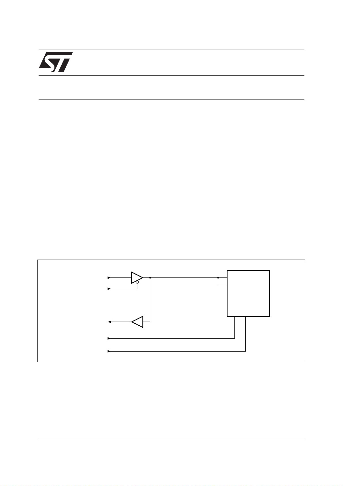
Figure 1. Typical Application of the Common-D/Q Approach
D Driver
Common D/Q Bus
Data In
Driver Enable
(active low)
Q Receiver
Data Out
Clock In
Chip Select In
EEPROM Device
D
Q
CS
Ai02419
READ INSTRUCTION
The D driver and the Q receiver, in Figure 1, can be discrete logic, or part of a microcontroller I/O port, or
any equivalent circuit ry. The READ command and its address bits are clocked into the chi p, th rough the
D pin, on the rising edges of the C clock. Each bit must be kept valid for a minimum hold time (tDVCH) as
specified in the data sheet for the memory device. The device holds the Q pin in the high impedance state
during most of the input operation. However, as Figure 2 shows, the Q pin is taken out of this state at the
1/10June 1998
AN394 - APPLICATION NOTE
start of the last address bit (A0) of the instruction (signalle d by t he rising edge of C ), and starts to output
the leading zero that precedes the 16-bit data string. The data sheets specify the maximum delay (tCHQL)
between the rising edge of C and the leading zero data bit.
Figure 2. Timing Sequence for a Read Instruction
C
S
D
Q
1
1 0 A5 A4 A3 A2 A1 A0
High Impedance
0
Bus Conflict
D15 D14 D13 D12 D11 D10 D9
Ai02420
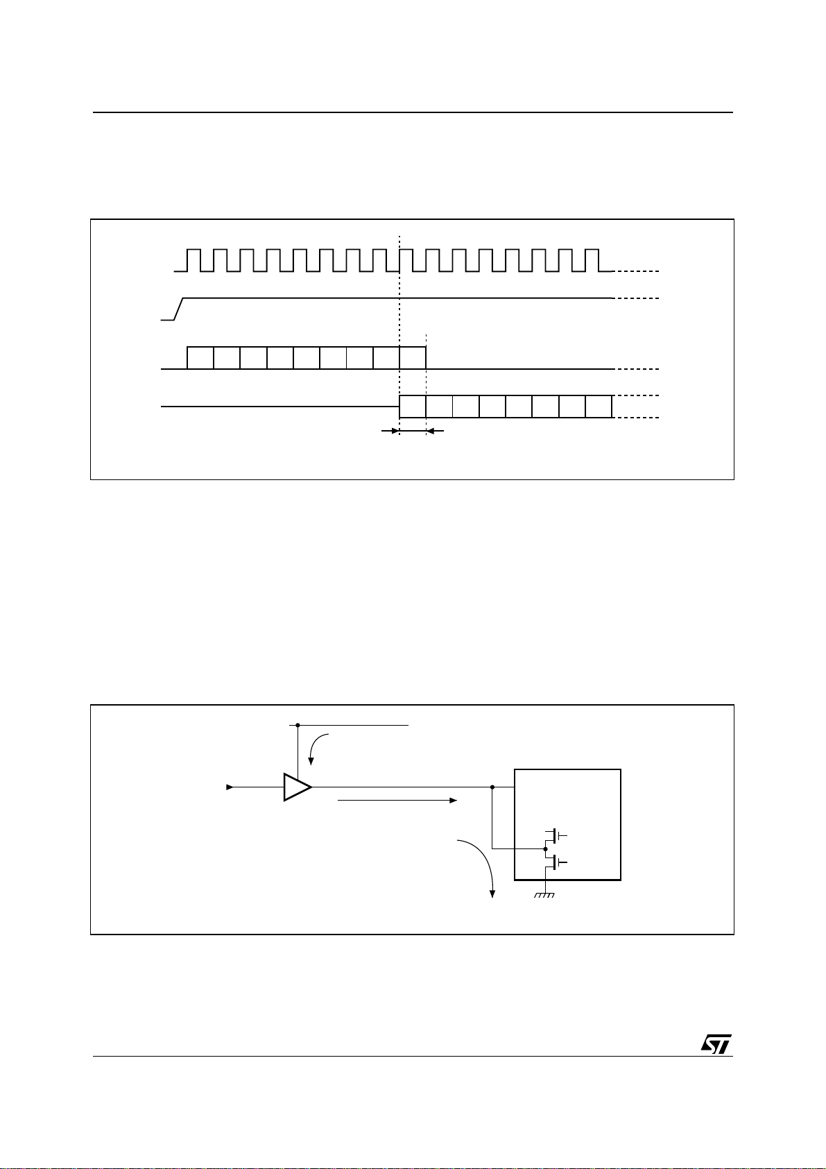
Since the D driver must remain ena bled with the A0 bit for a minimum of tDVCH (t he hold time), a bus
conflict occurs whenever the A0 bit is a “1”, as it would be for all odd addressed registers). The consequences are:
– A low impedance path is created between Vcc and ground through the D driver and the on-chip Q output
buffer (as depicted in Figure 3). This short-circuit may produce glitches on the power supply which can
disturb all the circuits on the board.
– The logic level on the D/Q bus is not well-defi ned: the potent ial divider chain, so created, can end up
producing a voltage level anywhere between Vcc and 0 V. Thus access to the odd addressed registers
will probably be impossible.
Figure 3. Short-Circuit Created Between Vcc and Ground
V
CC
D Driver
Common D/Q Bus
A0="1"
EEPROM Device
D
2/10
Low Impedance Path
Q
Output
Buffer
Ai02424
AN394 - APPLICATION NOTE
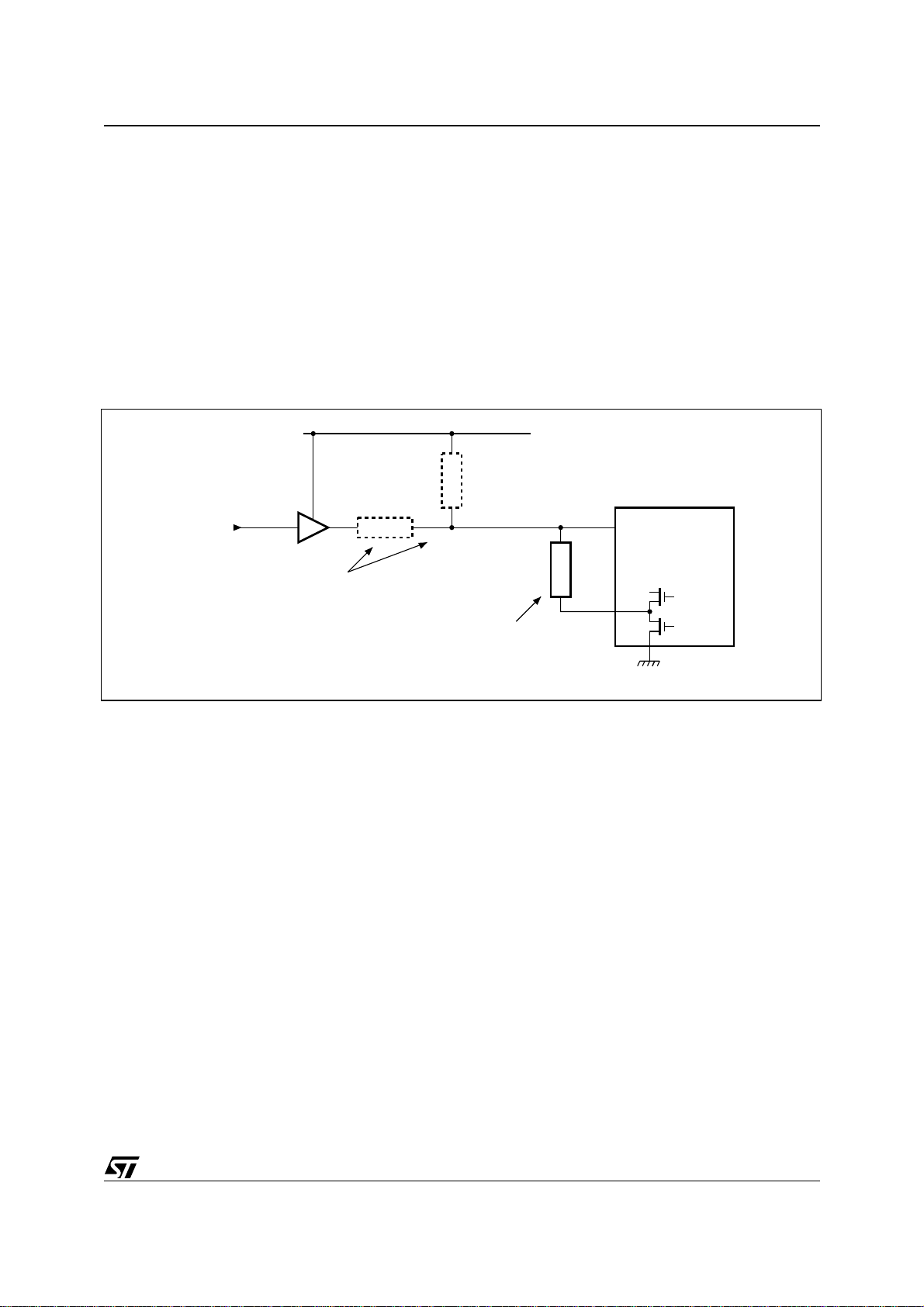
This problem can be avoided by inserting a current limiting resistor in the current sink path. Figure 4 shows
some possible locations for this resistor. However, the best location is between the Q output and the D/Q
bus for the following reasons:
– During the overlap time, only the D driver is providing useful information. The Q driver simply outputs a
constant zero. By p lacing th e resist or i n this position, the D driver overrides t he Q driver at setting the
logic level on the D/Q bus, thereby allowing the last address bit to be presented on the D p in for the
specified hold time (tDVCH).
– The R resistor slows down the propagat ion time of the Q output signals on the D/Q bus, as discussed
later in this document. In this position, the resistor only slows down the transmission of the 16 bits of
data during a READ operation. If R were in series with the D drive r, all operations would be slowed
down.
Figure 4. Possible Locations for the Current Limiting Resistor
V
CC
(If D driver is an
open collector type)
R
Recommended
Location
EEPROM Device
D
Q
Output
Buffer
Ai02421
A0="1"
D Driver
R
R
Not Recommended
Locations
The R resistor does not have any effect as long as Q is in its high impedance state. During the execution
of a READ instruc tion, R s in ks s ome current f rom th e D driver during the short overlap time. Then t he D
driver is disabled and Q output takes control of the D/Q bus through the R resistor.
Because of the bus capacitance, C, the signals are distorted, as shown in Figure 5 (on the next page): the
rising and falling edges of the Q output are transformed into exponential curves whose shape depends on
the time constant RC.
3/10

AN394 - APPLICATION NOTE
Figure 5. Exponential Charge and Discharge of the Bus Capacitance
% of the
Voltage Swing
95%
86%
63%
37%
13%
5%
0 RC 2xRC 3xRC
RC = Time Constant
0 RC 2xRC 3xRC
Ai02422
As a consequence, the logic level on the D/Q bus is not stable until some time after the rising edge of the
C clock. The delay in reading the bus should be at least 3xRC.
In a typical data sheet for a 5 V device, VOH(min) = 2.4 V and VOL(max) = 0.4 V, so giving a voltage swing
of 2 V. Using the 3xRC approximation, the D/Q bus levels will be:
– logical “1” = 2.3 V minimum after a delay of 3xRC
– logical “0” = 0.5 V maximum after the C rising edge
It might be necessary to reduce the C clock frequency, when shifting the 16 data bits out from the EEP-
ROM during a READ operation, by an amount that is directly related to the RC time constant of the D/Q
bus. All other operations can be performed at the nominal clock rate.
Figures 6, 7, 8 show some experimental exampl es, plotted from the oscillosc ope, with different va lues of
R and C. In the last example, the maximum clock frequency is: 1/(3xRC) = 100 kHz, assuming that the D/
Q bus is sampled by the Q receiver circuitry just before the rising edge of the C clock.
4/10

Figure 6. Oscilloscope Plot, R = 10 kΩ, C = 100 pF, RC = 1 µs
AN394 - APPLICATION NOTE
Ai02425
AO bit
is '1'
Q output
a '0' bit
D/Q bus is now driven by Q
D driver is disabled here
Figure 7. Oscilloscope Plot, R = 5 kΩ, C = 100 p F, RC = 500 ns
10 µS
5V
C clock
D/Q bus
Q output
D driver enable
(1 = disabled)
5/10

AN394 - APPLICATION NOTE
Figure 8. Oscilloscope Plot, R = 10 kΩ, C = 330 pF, RC = 3.3 µs
Ai02427
10 µS
5V
C clock
D/Q bus
Q output
D driver enable
(1 = disabled)
In order to avoid over reducing the clock frequency, the following techniques can be used to minimize the
R and C values:
■ To minimize the bus capacitance:
– the EEPROM device should be position as close as possible to the D-driver/Q-receiver circuitry (the ca-
pacitance is proportional to the surface area of the bus line).
– As few devices as possible should share the D/Q bus (the capacitance is proportional to the number of
input gates connected to the bus).
■ To minimize the resistor value:
– Find, from the data sheet, the maximum current that the D driver can source, and divide this value into
the value of Vcc.
– Find the maximum transient current that the power supply can source without glitches being introduced
on to the power lines, and divide this value into the value of Vcc.
– It is up to the designer to decide the best trade-off, based upon his specific application’s requirements,
but the resistor value should not be less than the higher of the two values calculated above.
INTERFACE WITH CMOS CIRCUITS
The MICROWIRE EEPROM spec ification makes these devices compa tible with TTL input/output levels.
When interfacing these devices to CMOS circui ts, howe ve r, s ome precaut ion s m ust be ta ken, to ens ure
the correct interpretation of the logic levels.
Since the output-high level is close to VCC, and the output-low level is close to 0 V, there are no difficulties
in driving the D, S and C inputs of the EEPROM devices.
For the Q ou tput, though, the minimum output-high l ev el is specified as being 2.4 V, which is lower than
the minimum input-high level of CMOS (3.5 V for Vcc = 5 V). A common practice is to connect a pull-up
resistor, Rp, between the Q output and Vcc.
This solution works well when D and Q a re s eparate. However, it raises some difficulties when D and Q
are tied together.
6/10

AN394 - APPLICATION NOTE
When the Q output is at a “zero” level (VOL= 0.4 V), during the overlap period, the R and Rp resistors form
a potential divider chain, as shown in Figure 9. Rp must have a resistance greater than 5 times that of R.
This means that the “zero” level on the D/Q bus is: 0.4 V + (5 V -0.4 V) x R / (R + Rp) = 1.17 V. Although
this value is 330 mV below the 1.5 V maximum input-low level for CMOS, it does mean losing the wide
noise margin that is traditionally associated with the CMOS specification.
Figure 9. D/Q Bu s Configu ration with Pull-up Resistor (R p)
V
CC
R
D Driver
(CMOS)
Data In
P
EEPROM Device
D
Driver Enable
(active low)
Q Receiver
(CMOS)
Data Out
R
Q
Output
Buffer
Ai02423
For a high to low transition, the Q on-chip output buffer has to discharge the bus capacitance through the
R resistor and to sink some current from Vcc through the Rp resistor. The new time constant, when compared to that calculated earlier in this document, is reduced by 17%, because of the parallel combination
of R and Rp. However, the steady low level is not 0.4 V, as had been assumed for TTL levels, but 1.17 V,
as calculated above for Rp = 5xR. Despite this smaller time constant, the voltage swing between high and
low is greater in this case, as d escribed la ter in t his do cumen t, so i t is advisabl e to k eep the sam e del ay
(3xRC) between the C clock rising edge and the first sampling of the data line.
A greater problem is faced during the low to high transition, though. At first, the bus capacitance is charged
by the Q output through R, and from the Vcc power supply via Rp, again leading to a time constant for Rp
connected in parallel with R. But once the D/Q bus reaches the Q output voltage level, the Q on-chip buffer
automatically turns off, and the Rp resistor remains the only contributor to the charge of the bus capacitance. This results in a much higher time constant: RpxC =5xRC.
For the worst case output-high level for Q (VOH= 2.4 V), combined with the minimum input-high level for
CMOS, the charging delay, after the Q driver cuts out, needs t o be at least 0.55xRpC: that is, 2.75xRC.
This is still assuming Vcc = 5 V, and allowing for a noise margin of 300 or 400 mV.
As a result, the minimum delay be tween the rising edge of C and the sampling of the D/Q bus sh ould be
2 or 3 times longer than t he o ne we have found for the TTL level s (without Rp), and t he clo ck frequ ency
must be reduced accordingly. (A typical oscilloscope plot is shown in Figure 10).
It is possible to avoid this situation by using a TTL-compatible CMOS device as the Q receiver circuit, and
thereby to remove the need for the Rp resistor. Suitable devices include:
■ members of the 74HCTXXX family
■ a CMOS microcontroller that provides an option for “TTL input levels” on its I/O ports, such as the ST9
series.
7/10

AN394 - APPLICATION NOTE
Figure 10. Oscilloscope Plot, R = 10 kΩ, C = 100 pF, Rp = 50 kΩ
Ai02428
10 µS
5V
C clock
D/Q bus
Q output
D driver enable
(1 = disabled)
PROGRAMMING MODE: ACKNOWLEDGEMENT OF READY/BUSY STATUS
During a self-time d progr am min g cycle , MICROWIRE EEPRO M device s us e the Q output to indi ca te th e
ready/busy status of the chip. This occurs during the execution of comma nds such as: WRITE, E RASE,
WRAL and ERAL.
The self-timed programming cycle begin s with the falling edge of S, at the end of a programming command. The S pin must be kept low for a minimum of tSLSH (as described in the data sheet). T he Q output
remains in its high impedance state as long as S is low. If S is brought high for clocking-in a new command,
Q comes out of its high impedance state, and indi cates the Ready/Busy status of t he chip (0 = Busy,
1 = Ready).
Figure 11. Acknowledgement of the Ready/Busy Signal on the Q Output
8/10
Ai02429
10 µS
5V
C clock
D/Q bus
D driver enable
(1 = disabled)

AN394 - APPLICATION NOTE
In applications where D and Q are tied toget her, t his m ay a gain crea te bus c onflicts . Theref ore, it i s rec ommended that this s tatus sig nal be c ancelle d as s oon as possible: this can be achieved very simply by
applying a single clock pulse on the C input while S is high, as depicted in Figure 11.
The operation is scheduled as follows:
– shift the write command into the chip
– bring S low for the minimum period of tSLSH
– bring S high
– monitor the D/Q bus until a high level (Ready) is detected
–clock C once
– bring S low
– the chip i s now re ady to accept the n ext instruction
It should also be noted that, on power-up, the Ready/Busy status be initially in the active state. Therefore,
it is recommended to clock C once (with S = 1) prior to the issue of the first command.
IMPROVING ON THE CALCULATIONS IN THIS DOCUMENT
This document has discussed how MICROWIRE devices can be used in a configuration in which the D
and Q lines are tied together as a single bus. For safety, and for generality, the worst case and most conservative conditions have been assumed in all calculations.
In particular circumstances, however, it might be possible for the design er to do better than this. In the
designer’s own particular application, it might be reasonable to rule out some worst-case situations as never occurring, and to adapt the calculations accordingly.
9/10

AN394 - APPLICATION NOTE
If you have any qu estions or sugg estions concerning t he matters raised i n this document, pl ease send
them to the following electronic mail address:
apps.eeprom@st.com
Please remember to include your name, company, location, telephone numbe r and fax numbe r.
Information furnished is believed to be accurate and reliable. However, STMicroelectronics assumes no responsibility for the consequences
of use of such information nor for any infringement of patents or other rights of third parties which may result from its use. No license is granted
by implic ation or otherwise und er any patent or patent ri ghts of STMi croelectronics. Speci f i cations menti oned in this publicatio n are subjec t
to change without notice. Th i s publication sup ersedes and repl aces all information previousl y supplied. STMicroelectronics products are not
authori zed for use as criti cal component s in life support devices or sys tems without ex press written approval of STM i croelectroni cs.
© 1998 STM i croelectroni cs - All Right s Reserved
The ST log o i s a registered trademark of STM i croelectronics.
All other nam es are the property of their respective owne rs.
STMicroelectronics GROUP OF COMPANIES
Austra lia - Brazil - China - France - Ger m any - Italy - Japan - Korea - Malaysia - Malta - Morocco - The N et herlands - Singapore - Spain -
Sweden - Switzerland - Taiwan - Thailand - United Kingdom - U.S.A.
10/10
 Loading...