

Page 1

1 Introduction
For designers of STM32 microcontroller applications, it is important to be able to easily
replace one microcontroller type by another one in the same product family. Migrating an
application to a different microcontroller is often needed, when product requirements grow,
putting extra demands on memory size, or increasing the number of I/Os. On the other
hand, cost reduction objectives may force you to switch to smaller components and shrink
the PCB area.
This application note is written to help you and analyze the steps you need to migrate from
an existing STM32F1 devices based design to STM32F2 devices. It groups together all the
most important information and lists the vital aspects that you need to address.
To migrate your application from STM32 F1 series to F2 series, you have to analyze the
hardware migration, the peripheral migration and the firmware migration.
AN3427
Application note
Migrating a microcontroller application
from STM32F1 to STM32F2 series
To benefit fully from the information in this application note, the user should be familiar with
the STM32 microcontroller family. Available from www.st.com.
● The STM32F1 family reference manuals (RM0008 and RM0041), the STM32F1
datasheets, and the STM32F1 Flash programming manuals (PM0075, PM0063 and
PM0068).
● The STM32F2 family reference manual (RM0033), the STM32F2 datasheets, and the
STM32F2 Flash programming manual (PM0059).
For an overview of the whole STM32 series and a comparision of the different features of
each STM32 product series, please refer to AN3364 'Migration and compatibility guidelines
for STM32 microcontroller applications'
July 2011 Doc ID 019001 Rev 1 1/52
www.st.com
Page 2

Contents AN3427
Contents
1 Introduction . . . . . . . . . . . . . . . . . . . . . . . . . . . . . . . . . . . . . . . . . . . . . . . . 1
2 Hardware migration . . . . . . . . . . . . . . . . . . . . . . . . . . . . . . . . . . . . . . . . . . 6
3 Peripheral migration . . . . . . . . . . . . . . . . . . . . . . . . . . . . . . . . . . . . . . . . . 9
3.1 STM32 product cross-compatibility . . . . . . . . . . . . . . . . . . . . . . . . . . . . . . 9
3.2 System architecture . . . . . . . . . . . . . . . . . . . . . . . . . . . . . . . . . . . . . . . . . 12
3.2.1 32-bit multi-AHB bus matrix . . . . . . . . . . . . . . . . . . . . . . . . . . . . . . . . . . 12
3.2.2 Adaptive real-time memory accelerator (ART Accelerator™) . . . . . . . . 12
3.2.3 Dual SRAM . . . . . . . . . . . . . . . . . . . . . . . . . . . . . . . . . . . . . . . . . . . . . . 13
3.3 Memory mapping . . . . . . . . . . . . . . . . . . . . . . . . . . . . . . . . . . . . . . . . . . . 13
3.4 RCC . . . . . . . . . . . . . . . . . . . . . . . . . . . . . . . . . . . . . . . . . . . . . . . . . . . . . 16
3.5 DMA . . . . . . . . . . . . . . . . . . . . . . . . . . . . . . . . . . . . . . . . . . . . . . . . . . . . . 23
3.5.1 Interrupts . . . . . . . . . . . . . . . . . . . . . . . . . . . . . . . . . . . . . . . . . . . . . . . . 26
3.6 GPIO . . . . . . . . . . . . . . . . . . . . . . . . . . . . . . . . . . . . . . . . . . . . . . . . . . . . 29
3.6.1 Alternate function mode . . . . . . . . . . . . . . . . . . . . . . . . . . . . . . . . . . . . . 30
3.7 EXTI source selection . . . . . . . . . . . . . . . . . . . . . . . . . . . . . . . . . . . . . . . 31
3.8 FLASH . . . . . . . . . . . . . . . . . . . . . . . . . . . . . . . . . . . . . . . . . . . . . . . . . . . 31
3.9 ADC . . . . . . . . . . . . . . . . . . . . . . . . . . . . . . . . . . . . . . . . . . . . . . . . . . . . . 33
3.10 PWR . . . . . . . . . . . . . . . . . . . . . . . . . . . . . . . . . . . . . . . . . . . . . . . . . . . . . 35
3.11 RTC . . . . . . . . . . . . . . . . . . . . . . . . . . . . . . . . . . . . . . . . . . . . . . . . . . . . . 36
3.12 Miscellaneous . . . . . . . . . . . . . . . . . . . . . . . . . . . . . . . . . . . . . . . . . . . . . . 37
3.12.1 Ethernet PHY interface selection . . . . . . . . . . . . . . . . . . . . . . . . . . . . . . 37
3.12.2 TIM2 internal trigger 1 (ITR1) remapping . . . . . . . . . . . . . . . . . . . . . . . 37
4 Firmware migration using the library . . . . . . . . . . . . . . . . . . . . . . . . . . 38
4.1 Migration steps . . . . . . . . . . . . . . . . . . . . . . . . . . . . . . . . . . . . . . . . . . . . . 38
4.2 RCC . . . . . . . . . . . . . . . . . . . . . . . . . . . . . . . . . . . . . . . . . . . . . . . . . . . . . 38
4.3 FLASH . . . . . . . . . . . . . . . . . . . . . . . . . . . . . . . . . . . . . . . . . . . . . . . . . . . 40
4.4 GPIO . . . . . . . . . . . . . . . . . . . . . . . . . . . . . . . . . . . . . . . . . . . . . . . . . . . . 43
4.4.1 Output mode . . . . . . . . . . . . . . . . . . . . . . . . . . . . . . . . . . . . . . . . . . . . . 43
4.4.2 Input mode . . . . . . . . . . . . . . . . . . . . . . . . . . . . . . . . . . . . . . . . . . . . . . . 43
4.4.3 Analog mode . . . . . . . . . . . . . . . . . . . . . . . . . . . . . . . . . . . . . . . . . . . . . 43
2/52 Doc ID 019001 Rev 1
Page 3

AN3427 Contents
4.4.4 Alternate function mode . . . . . . . . . . . . . . . . . . . . . . . . . . . . . . . . . . . . . 43
4.5 EXTI . . . . . . . . . . . . . . . . . . . . . . . . . . . . . . . . . . . . . . . . . . . . . . . . . . . . . 45
4.6 DMA . . . . . . . . . . . . . . . . . . . . . . . . . . . . . . . . . . . . . . . . . . . . . . . . . . . . . 46
4.7 ADC . . . . . . . . . . . . . . . . . . . . . . . . . . . . . . . . . . . . . . . . . . . . . . . . . . . . . 47
4.8 Backup data registers . . . . . . . . . . . . . . . . . . . . . . . . . . . . . . . . . . . . . . . . 49
4.9 Miscellaneous . . . . . . . . . . . . . . . . . . . . . . . . . . . . . . . . . . . . . . . . . . . . . . 49
4.9.1 Ethernet PHY interface selection . . . . . . . . . . . . . . . . . . . . . . . . . . . . . . 49
4.9.2 TIM2 internal trigger 1 (ITR1) remapping . . . . . . . . . . . . . . . . . . . . . . . 50
5 Revision history . . . . . . . . . . . . . . . . . . . . . . . . . . . . . . . . . . . . . . . . . . . 51
Doc ID 019001 Rev 1 3/52
Page 4

List of tables AN3427
List of tables
Table 1. STM32 F1 series and STM32 F2 series pinout differences . . . . . . . . . . . . . . . . . . . . . . . . . 6
Table 2. STM32 peripheral compatibility analysis F1 versus F2 series . . . . . . . . . . . . . . . . . . . . . . . 9
Table 3. IP bus mapping differences between STM32 F1 and STM32 F2 series. . . . . . . . . . . . . . . 13
Table 4. RCC differences between STM32 F1 and STM32 F2 series . . . . . . . . . . . . . . . . . . . . . . . 16
Table 5. Example of migrating system clock configuration code from F1 to F2 series . . . . . . . . . . . 20
Table 6. RCC registers used for peripheral access configuration. . . . . . . . . . . . . . . . . . . . . . . . . . . 21
Table 7. DMA request differences between STM32 F1 series and STM32 F2 series . . . . . . . . . . . 23
Table 8. Interrupt vector differences between STM32 F1 series and STM32 F2 series . . . . . . . . . . 27
Table 9. GPIO differences between STM32 F1 series and STM32 F2 series . . . . . . . . . . . . . . . . . 30
Table 10. FLASH differences between STM32 F1 series and STM32 F2 series . . . . . . . . . . . . . . . . 32
Table 11. ADC differences between STM32 F1 series and STM32 F2 series . . . . . . . . . . . . . . . . . . 33
Table 12. PWR differences between STM32 F1 series and STM32 F2 series. . . . . . . . . . . . . . . . . . 35
Table 13. STM32F10x and STM32F2xx FLASH driver API correspondence . . . . . . . . . . . . . . . . . . . 41
Table 14. Document revision history . . . . . . . . . . . . . . . . . . . . . . . . . . . . . . . . . . . . . . . . . . . . . . . . . 51
4/52 Doc ID 019001 Rev 1
Page 5

AN3427 List of figures
List of figures
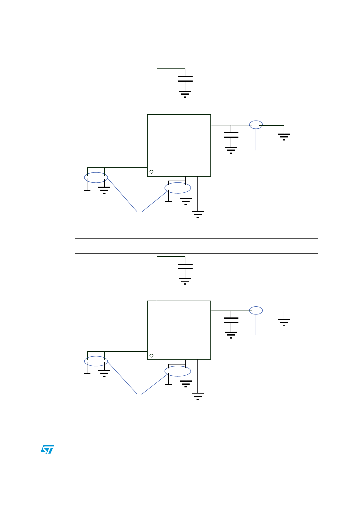
Figure 1. Compatible board design: LQFP144 . . . . . . . . . . . . . . . . . . . . . . . . . . . . . . . . . . . . . . . . . . 7
Figure 2. Compatible board design: LQFP100 . . . . . . . . . . . . . . . . . . . . . . . . . . . . . . . . . . . . . . . . . . 7
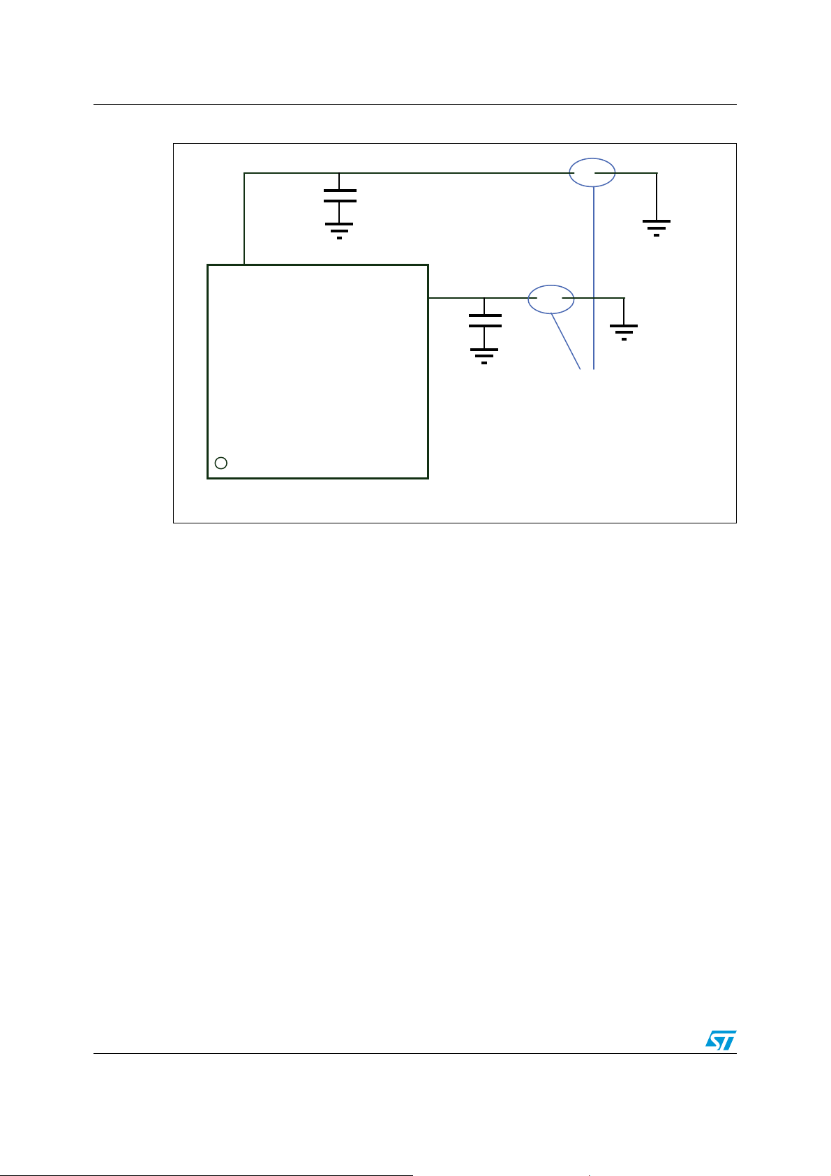
Figure 3. Compatible board design: LQFP64 . . . . . . . . . . . . . . . . . . . . . . . . . . . . . . . . . . . . . . . . . . . 8
Figure 4. STM32 F2 series system architecture . . . . . . . . . . . . . . . . . . . . . . . . . . . . . . . . . . . . . . . . 12
Doc ID 019001 Rev 1 5/52
Page 6

Hardware migration AN3427
2 Hardware migration
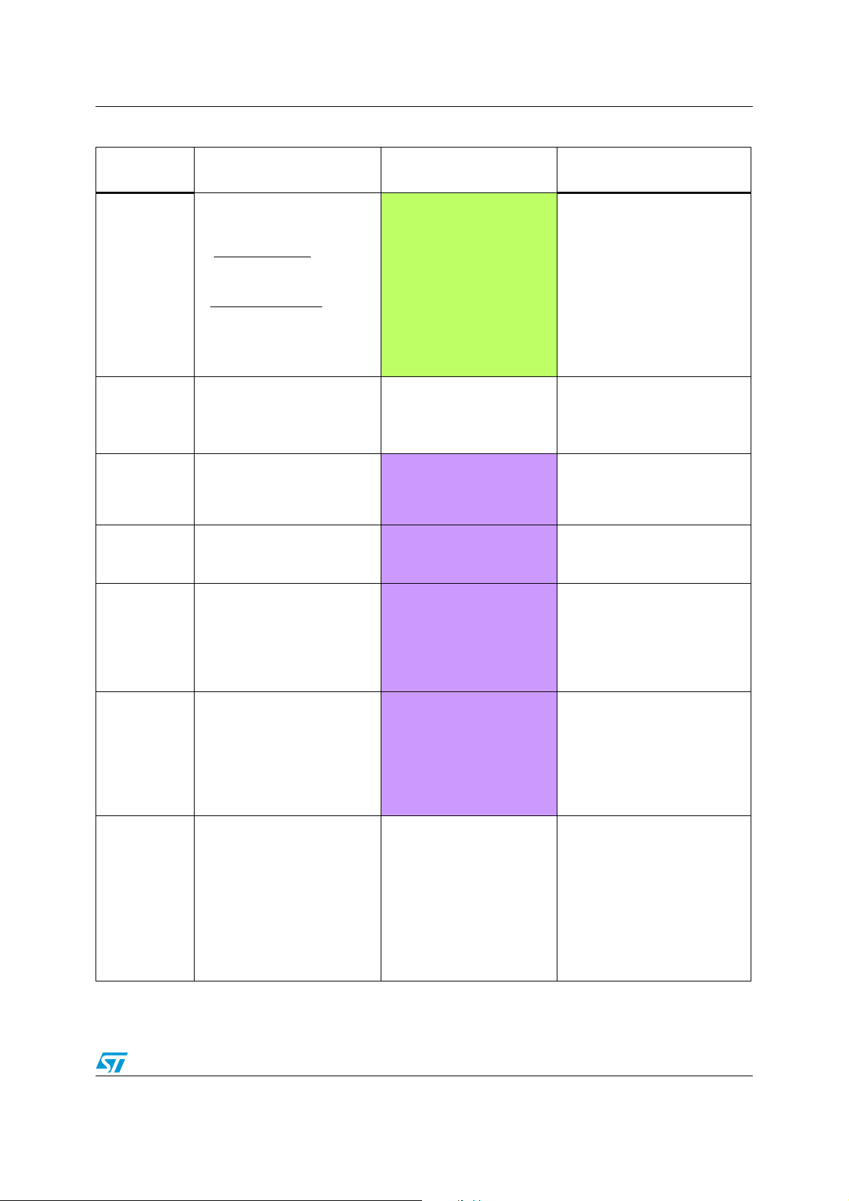
All peripherals shares the same pins in the two families, but there are some minor
differences between packages.
In fact, the STM32 F2 series maintains a close compatibility with the whole STM32 F1
series. All functional pins are pin-to-pin compatible. The STM32 F2 series, however, are not
drop-in replacements for the STM32 F1 series: the two families do not have the same power
scheme, and so their power pins are different. Nonetheless, transition from the STM32 F1
series to the STM32 F2 series remains simple as only a few pins are impacted (impacted
pins are in bold in the table below).
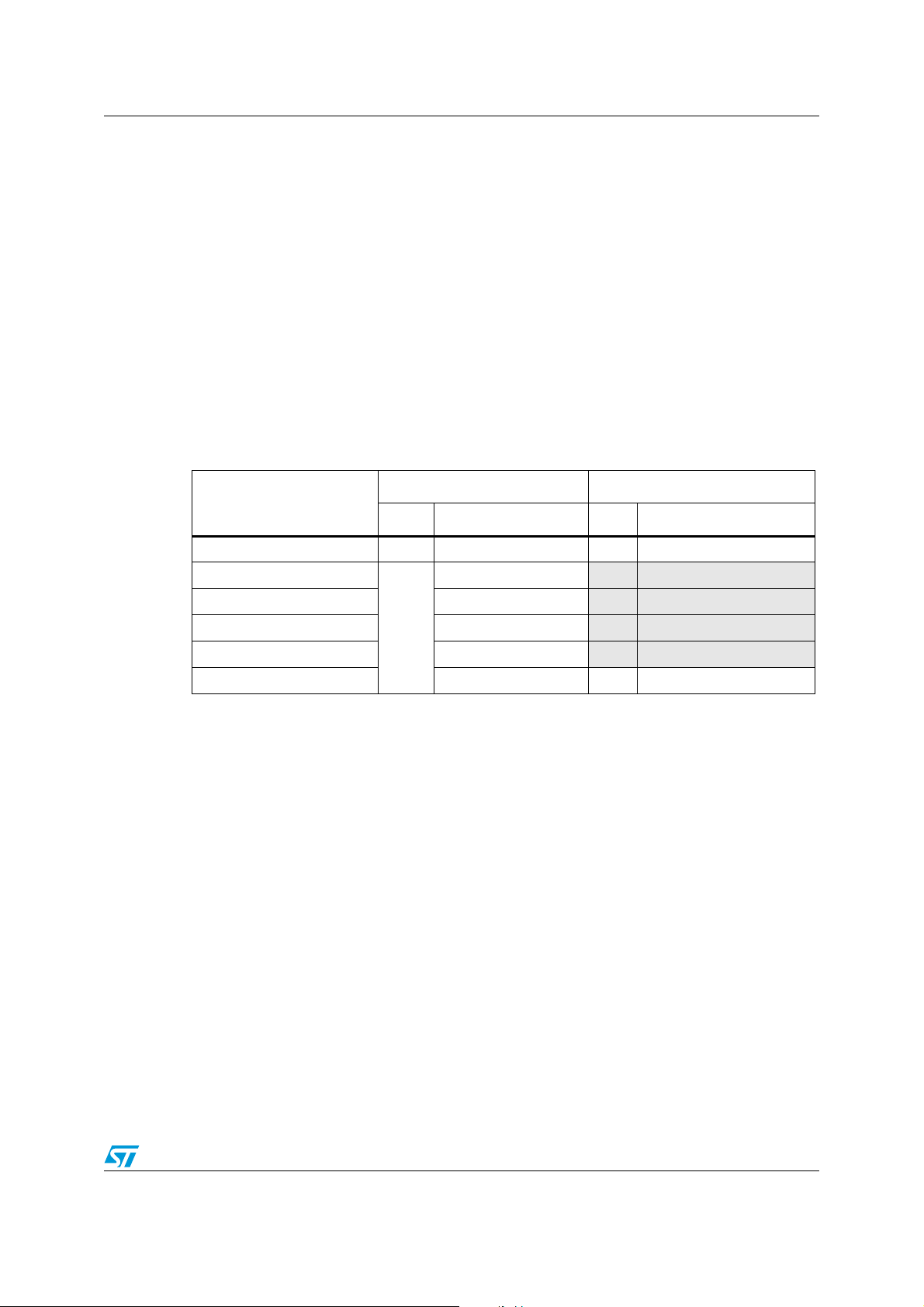
Table 1. STM32 F1 series and STM32 F2 series pinout differences
QFP64 QFP100 QFP144 Pinout QFP64 QFP100 QFP144 Pinout
51223PD0 - OSC_IN 5 12 23 PH0 - O SC_ IN
61324PD1 - OSC_OUT 6 13 24 PH1 - O S C _ O U T
12 19 30 VSSA 19 30 VDD
STM32 F1 series STM32 F2 series
20 31 VREF- 12 20 31 VSSA
31 49 71 VSS_1 31 49 71 VCAP1
73 106 NC 47 73 106 VCAP2
47 74 107 VSS_2 74 107 VSS2
63 99 143 VSS_3 63 VSS_3
The figures below show examples of board designs that are compatible with both the F1 and
the F2 series.
6/52 Doc ID 019001 Rev 1
Page 7
AN3427 Hardware migration
AIC
6
$$
6
33
6
33
RESISTORORSOLDERINGBRIDGE
PRESENTFORTHE34-&XXX
CONFIGURATIONNOTPRESENTINTHE
34-&XXXCONFIGURATION
4WO RESISTORSCONNECTEDTO
2&5
6$$633OR.#FORTHE34-&XX
6
$$
FORFUTUREPRODUCTS
PS7
33
Ȱ
Ȱ
6
33
6
33
6
33
6
$$
6
33
633FORTHE34-&X
AIB
6
$$
6
33
6
33
RESISTORORSOLDERINGBRIDGE
PRESENTFORTHE34-&XXX
CONFIGURATIONNOTPRESENTINTHE
34-&XXXCONFIGURATION
4WO RESISTORSCONNECTEDTO
2&5
6$$633OR.#FORTHE34-&XX
6
$$
FORFUTUREPRODUCTS
PS7
33
Ȱ
Ȱ
6
33
6
33
6
33
6
$$
6
33
Figure 1. Compatible board design: LQFP144
Figure 2. Compatible board design: LQFP100
Doc ID 019001 Rev 1 7/52
Page 8
Hardware migration AN3427
½RESISTORORSOLDERINGBRIDGE
AI
6
33
6
33
6
33
6
33
Ȱ
½
PRESENTFORTHE34-&XXX
CONFIGURATIONNOTPRESENTINTHE
34-&XXXCONFIGURATION
Figure 3. Compatible board design: LQFP64
8/52 Doc ID 019001 Rev 1
Page 9

AN3427 Peripheral migration
3 Peripheral migration
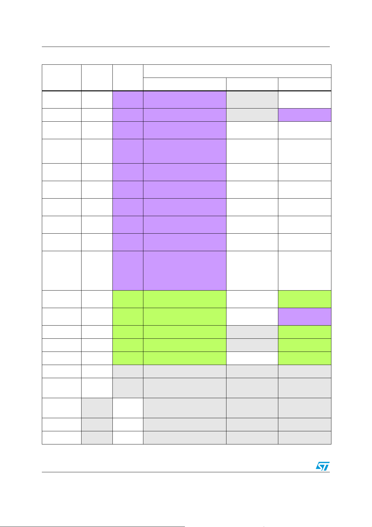
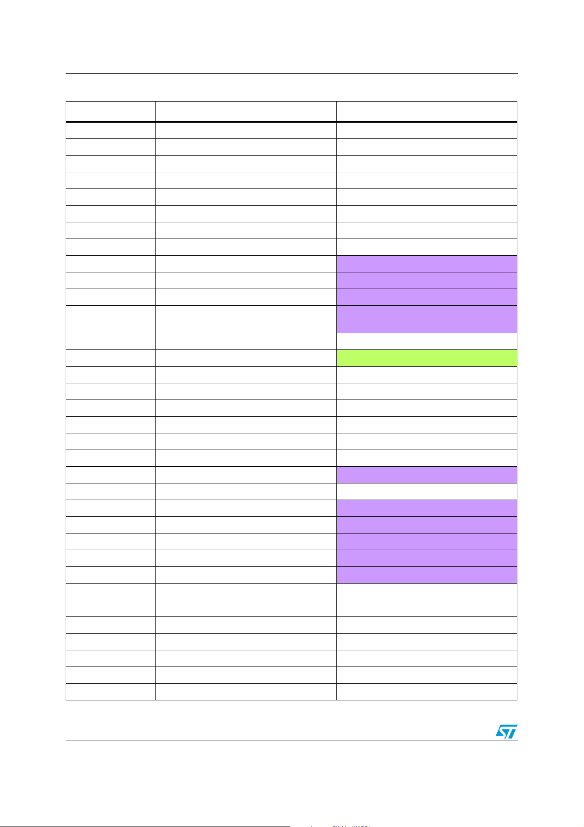
As shown in Table 2 on page 9, there are three categories of peripherals. The common
peripherals are supported with the dedicated firmware library without any modification,
except if the peripheral instance is no longer present, you can change the instance and of
course all the related features (clock configuration, pin configuration, interrupt/DMA
request).
The modified peripherals such as: FLASH, ADC, RCC, DMA, GPIO and RTC are different
from the F1 series ones and should be updated to take advantage of the enhancements and
the new features in F2 series.
All these modified peripherals in the F2 series are enhancements in performance and
features designed to meet new market requirements and to fix some limitations present in
the F1 series.
3.1 STM32 product cross-compatibility
The STM32 series embeds a set of peripherals which can be classed in three categories:
● The first category is for the peripherals which are by definition common to all products.
Those peripherals are identical, so they have the same structure, registers and control
bits. There is no need to perform any firmware change to keep the same functionality at
the application level after migration. All the features and behavior remain the same.
● The second category is for the peripherals which are shared by all products but have
only minor differences (in general to support new features), so migration from one
product to another is very easy and does not need any significant new development
effort.
● The third category is for peripherals which have been considerably changed from one
product to another (new architecture, new features...). For this category of peripherals,
migration will require new development at application level.
Ta bl e 2 below gives a general overview of this classification:
Table 2. STM32 peripheral compatibility analysis F1 versus F2 series
Peripheral F1 series F2 series
FSMC Yes Yes Same features Identical Full compatibility
WWDG
IWDG
DBGMCU
CRC
EXTI
CAN
Compatibility
Comments Pinout SW compatibility
Ye s Yes Same features NA Full compatibility
Ye s Yes Same features NA Full compatibility
Ye s Yes Same features NA Full compatibility
Ye s Yes Same features NA Full compatibility
Ye s Yes Same features Identical Full compatibility
Ye s Yes Same features Identical Full compatibility
Doc ID 019001 Rev 1 9/52
Page 10
Peripheral migration AN3427
Table 2. STM32 peripheral compatibility analysis F1 versus F2 series (continued)
Compatibility
Peripheral F1 series F2 series
Comments Pinout SW compatibility
PWR Ye s Ye s + Enhancement NA
RCC
SPI
USART Ye s Ye s +
I2C
TIM
DAC
Ethernet
SDIO Ye s Ye s + Limitation fix Identical
USB OTG FS Ye s Ye s +
RTC
ADC
Ye s Ye s + Enhancement NA Partial compatibility
Ye s Ye s + TI mode / Max baudrate Identical
Limitation fix / Max baudrate /
One Sample Bit / Oversampling
by 8
Ye s Ye s + Limitation fix Identical
Ye s Ye s +
Ye s Ye s + DMA underrun interrupt Identical
Ye s Ye s +
Ye s Yes++ New peripheral
Ye s Yes++ New peripheral
32-bit Counter in TIM2 and
TIM5
IEEE1588 v2 / Enhanced DMA
descriptor
- Dynamic trimming capability of
SOF framing period in Host
mode
- Embeds a VBUS sensing
control
Identical
Identical
Identical
Identical
Identical for the
same feature
Identical for the
same feature
Full compatibility for
the same feature
Full compatibility for
the same feature
Full compatibility for
the same feature
Full compatibility for
the same feature
Full compatibility for
the same feature
Full compatibility for
the same feature
Full compatibility for
the same feature
Full compatibility for
the same feature
Full compatibility for
the same feature
Not compatible
Partial compatibility
FLASH
DMA
GPIO
CEC
USB FS
Device
Crypto/hash
processor
RNG
DCMI
10/52 Doc ID 019001 Rev 1
Ye s Yes++ New peripheral NA Not compatible
Ye s Yes++ New peripheral NA Not compatible
Ye s Yes++ New peripheral Identical Not compatible
Ye s NA NA NA NA
Ye s NA NA NA NA
NA Ye s NA NA NA
NA Ye s NA NA NA
NA Ye s NA NA NA
Page 11
AN3427 Peripheral migration
Color key:
= New feature or new architecture (Yes++)
= Same feature, but specification change or enhancement (Yes+)
= Feature not available (NA)
Table 2. STM32 peripheral compatibility analysis F1 versus F2 series (continued)
Compatibility
Peripheral F1 series F2 series
Comments Pinout SW compatibility
USB OTG HS NA Ye s NA NA NA
SYSCFG
NA Ye s NA NA NA
Doc ID 019001 Rev 1 11/52
Page 12

Peripheral migration AN3427
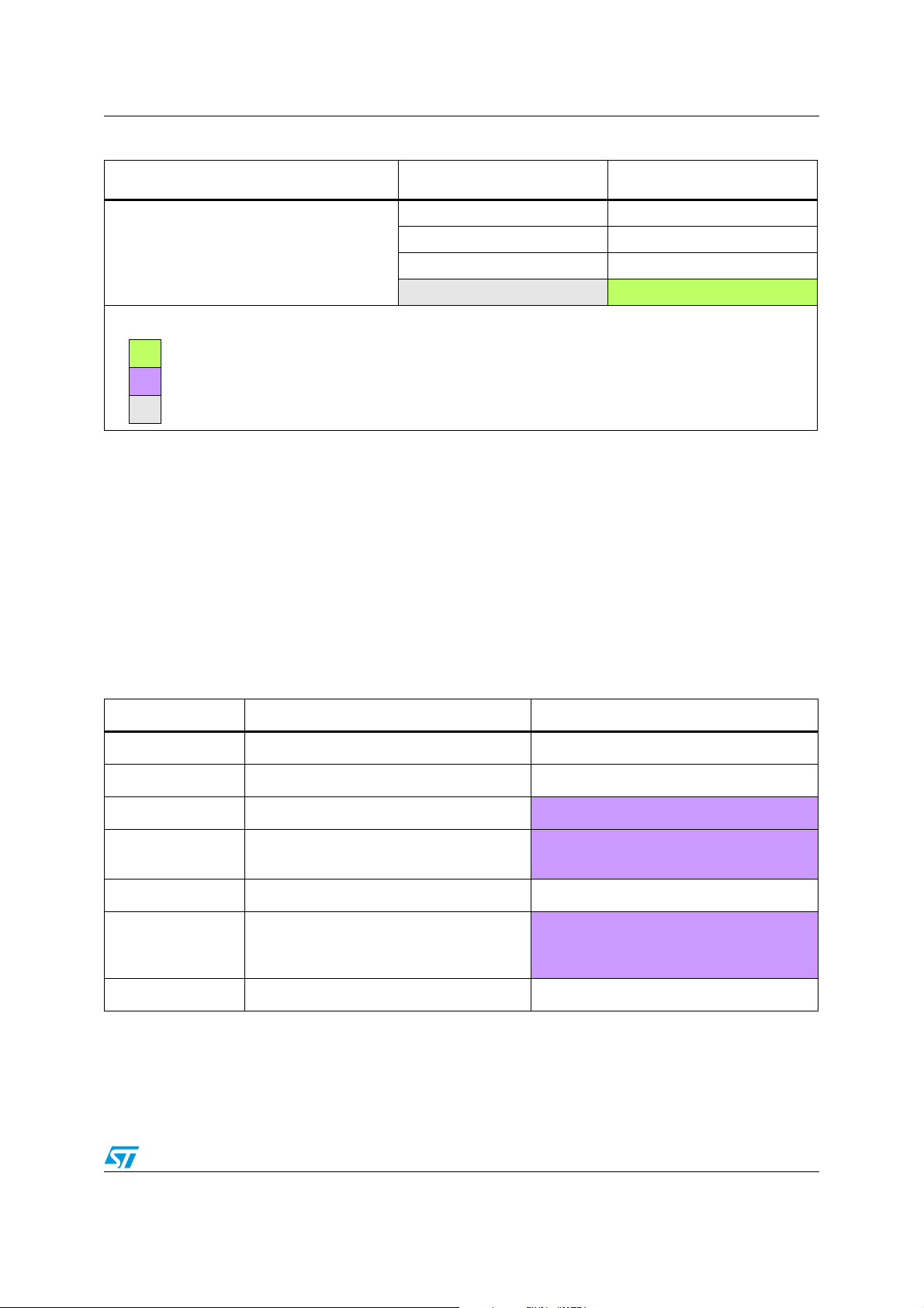
3.2 System architecture
STM32 F2 series are a new generation on STM32 with significant improvement in features
and performance with outstanding results: 150DMIPS at 120MHz and execution from Flash
equivalent to 0-wait state performance.
3.2.1 32-bit multi-AHB bus matrix
The 32-bit multi-AHB bus matrix interconnects all masters (CPU, DMA controllers, Ethernet,
USB HS) and slaves (Flash memory, 2 blocks of RAM, FSMC, AHB and APB peripherals)
and ensures seamless and efficient operation even when several high-speed peripherals
are working simultaneously. For instance, the core can access the Flash through the ART
Accelerator and the 112-Kbyte SRAM, while the DMA2 controller is transferring data from
the camera interface located on the AHB2 peripheral bus to an LCD connected to the
FSMC, and while the USB OTG High Speed interface is storing received data in the 16Kbyte SRAM block.
Figure 4. STM32 F2 series system architecture
3.2.2 Adaptive real-time memory accelerator (ART Accelerator™)
To free the full performance of the Cortex-M3 core, ST has developed a leading-edge 90 nm
process and a unique technology, the adaptive real-time ART Accelerator™. To release the
processor full 150 DMIPS performance at this frequency, the accelerator implements an
instruction prefetch queue and branch cache which increases program execution speed
from the 128-bit Flash memory. Based on the CoreMark benchmark, the performance
achieved thanks to the ART accelerator is equivalent to 0 wait state program execution from
Flash memory at a CPU frequency up to 120 MHz.
By default (after each device reset) the prefetch queue and branch cache are disabled, the
user can enable them using the PRFTEN, ICEN and DCEN bits in the FLASH_ACR register.
12/52 Doc ID 019001 Rev 1
Page 13
AN3427 Peripheral migration
3.2.3 Dual SRAM
The 128KB of SRAM is made of 2 blocks; one 112KB and one 16KB. Both can be accessed
simultaneously by 2 masters in 0 WS (CPU, DMAs, Ethernet, USB HS).
The 16KB SRAM can be used as a buffer for high speed peripherals like USB-HS, Ethernet,
Camera, without impacting the CPU performance.
3.3 Memory mapping
The peripheral address mapping has been changed in the F2 series vs. F1 series, the main
change concerns the GPIOs which have been moved to the AHB bus instead of the APB
bus to allow them to operate at maximum speed.
The tables below provide the peripheral address mapping correspondence between F2 and
F1 series.
Table 3. IP bus mapping differences between STM32 F1 and STM32 F2 series
STM32 F2 series STM32 F1 series
Peripheral
Bus Base address Bus Base address
FSMC Registers AHB3 0xA0000000 AHB 0xA0000000
RNG
0x50060800
NA NA
HASH 0x50060400
CRYP 0x50060000
DCMI 0x50050000
USB OTG FS 0x50000000 AHB 0x50000000
AHB2
NA NA
NA NA
NA NA
Doc ID 019001 Rev 1 13/52
Page 14
Peripheral migration AN3427
Table 3. IP bus mapping differences between STM32 F1 and STM32 F2 series
STM32 F2 series STM32 F1 series
Peripheral
Bus Base address Bus Base address
USB OTG HS
ETHERNET MAC 0x40028000
DMA2 0x40026400 0x40020400
DMA1 0x40026000 0x40020000
BKPSRAM 0x40024000
Flash interface 0x40023C00
RCC 0x40023800 0x40021000
CRC 0x40023000 0x40023000
GPIO I 0x40022000
GPIO H 0x40021C00
GPIO G 0x40021800
GPIO F 0x40021400 0x40011C00
GPIO E 0x40021000 0x40011800
GPIO D 0x40020C00 0x40011400
GPIO C 0x40020800 0x40011000
GPIO B 0x40020400 0x40010C00
GPIO A 0x40020000 0x40010800
TIM11
TIM10 0x40014400 0x40015000
TIM9 0x40014000 0x40014C00
EXTI 0x40013C00 0x40010400
AHB1
APB2
0x40040000 NA NA
0x40028000
AHB
NA NA
0x40022000
AHB
NA NA
NA NA
0x40012000
APB2
0x40014800 0x40015400
14/52 Doc ID 019001 Rev 1
Page 15
AN3427 Peripheral migration
Table 3. IP bus mapping differences between STM32 F1 and STM32 F2 series
STM32 F2 series STM32 F1 series
Peripheral
Bus Base address Bus Base address
SYSCFG
SPI1 0x40013000 APB2 0x40013000
SDIO 0x40012C00 AHB 0x40018000
ADC1 - ADC2 - ADC3 0x40012000 APB2
APB2
USART6 0x40011400
USART1 0x40011000
TIM8 0x40010400 0x40013400
TIM1 0x40010000 0x40012C00
DAC 0x40007400
PWR
CAN2 0x40006800 0x40006800
CAN1 0x40006400 0x40006400
I2C3 0x40005C00
I2C2 0x40005800
I2C1 0x40005400 0x40005400
UART5 0x40005000 0x40005000
UART4 0x40004C00 0x40004C00
0x40013800
0x40007000 0x40007000
NA NA
NA NA
APB2
APB1
NA NA
ADC3 - 0x40013C00
ADC2 - 0x40012800
ADC1 - 0x40012400
0x40013800
0x40007400
0x40005800
USART3 0x40004800 0x40004800
USART2 0x40004400 0x40004400
SPI3 / I2S3 0x40003C00 0x40003C00
SPI2 / I2S2 0x40003800 0x40003800
IWDG 0x40003000 0x40003000
WWDG 0x40002C00 0x40002C00
RTC
TIM14 0x40002000 0x40002000
TIM13 0x40001C00 0x40001C00
TIM12 0x40001800 0x40001800
TIM7 0x40001400 0x40001400
TIM6 0x40001000 0x40001000
TIM5 0x40000C00 0x40000C00
TIM4 0x40000800 0x40000800
APB1
APB1
0x40002800
(inc. BKP registers)
Doc ID 019001 Rev 1 15/52
0x40002800
Page 16
Peripheral migration AN3427
Color key:
= Same feature, but base address change
= Feature not available (NA)
Table 3. IP bus mapping differences between STM32 F1 and STM32 F2 series
STM32 F2 series STM32 F1 series
Peripheral
Bus Base address Bus Base address
TIM3
0x40000400
APB1
TIM2 0x40000000 0x40000000
APB1
BKP registers NA NA 0x40006C00
USB device FS
AFIO
NA NA 0x40005C00
NA NA APB2 0x40001000
3.4 RCC
The main differences related to the RCC (Reset and Clock Controller) in the STM32 F2
series vs. STM32 F1 series are presented in the table below.
Table 4. RCC differences between STM32 F1 and STM32 F2 series
RCC main
features
STM32 F1 series STM32 F2 series Comments
0x40000400
HSI 8 MHz RC factory-trimmed
LSI 40 KHz RC
16 MHz RC factory-trimmed
32 KHz RC
3 - 25 MHz
HSE
Depending on the product line
4 - 26MHz
used
LSE 32.768 KHz 32.768 kHz
No change to SW configuration:
– Enable/disable
RCC_CR[HSION]
– Status flag RCC_CR[HSIRDY]
No change to SW configuration:
– Enable/disable
RCC_CSR[LSION]
– Status flag
RCC_CSR[LSIRDY]
No change to SW configuration:
– Enable/disable
RCC_CR[HSEON]
– Status flag
RCC_CR[HSERDY]
No change to SW configuration:
– Enable/disable
RCC_BDCR[LSEON]
– Status flag
RCC_BDCR[LSERDY]
16/52 Doc ID 019001 Rev 1
Page 17
AN3427 Peripheral migration
Table 4. RCC differences between STM32 F1 and STM32 F2 series
RCC main
features
PLL
System clock
source
System clock
frequency
AHB
frequency
STM32 F1 series STM32 F2 series Comments
There is no change to PLL
enable/disable
RCC_CR[PLLON] and status
– Connectivity line:
+ 2 PLLs for I2S, Ethernet
and OTG FS clock
– Other product lines:
PLL
HSI, HSE or PLL HSI, HSE or PLL
up to 72 MHz depending on the
product line used
8 MHz after reset using HSI
up to 72 MHz
main PLL
main
– Main PLL for system, OTG
FS, SDIO and RNG clock
– Dedicated PLL for I2S
clock
120 MHz
16 MHz after reset using HSI
up to 120 MHz
flag RCC_CR[PLLRDY].
However, PLL configuration
(clock source selection,
multiplication/division factors)
are different. In F2 series a
dedicated register
RCC_PLLCFGR is used to
configure the PLL parameters.
No change to SW configuration:
– Selection bits
RCC_CFGR[SW]
– Status flag RCC_CFGR[SWS]
For STM32 F2, Flash wait states
must be adapted to the system
frequency depending on the
supply voltage range.
No change to SW configuration:
configuration bits
RCC_CFGR[HPRE]
APB1
frequency
APB2
frequency
RTC clock
source
up to 36 MHz
up to 72 MHz
LSI, LSE or HSE/128
up to 30 MHz
up to 60 MHz
LSI, LSE or HSE clock
divided by 2 to 31
No change to SW configuration:
configuration bits
RCC_CFGR[PPRE1].
In F2 series the PPRE1 bits
occupy bits [10:12], instead of
bits [8:10] in F1 series.
No change to SW configuration:
configuration bits
RCC_CFGR[PPRE2].
In F2 series the PPRE2 bits
occupy bits[13:15] of the
register, instead of bits [11:13] in
F1 series.
RTC clock source configuration
is done through the same bits
RCC_BDCR[RTCSEL] and
RCC_BDCR[RTCEN]. However,
in F2 series when HSE is
selected as RTC clock source,
additional bits are used in CFGR
register, RCC_CFGR[RTCPRE],
to select the division factor to be
applied on HSE clock.
Doc ID 019001 Rev 1 17/52
Page 18

Peripheral migration AN3427
Table 4. RCC differences between STM32 F1 and STM32 F2 series
RCC main
features
MCO clock
source
Internal
oscillator
measurement
/ calibration
Interrupt
STM32 F1 series STM32 F2 series Comments
MCO configuration in F2 series
is different from F1:
– For MCO1, the prescaler is
– MCO pin (PA8)
– Connectivity Line: HSI, HSE,
PLL/2, SYSCLK, PLL2, PLL3
or XT1
– Other product lines:
HSE, PLL/2 or SYSCLK
- LSI connected to TIM5 CH4
IC: can measure LSI w/ respect
to HSI/HSE clock
- CSS (linked to NMI IRQ)
- LSIRDY, LSERDY, HSIRDY,
HSERDY, PLLRDY, PLL2RDY
and PLL3RDY (linked to RCC
global IRQ)
HSI,
– MCO1 pin (PA8): HSI,
HSE, LSE or PLL
– MCO2 pin (PC9)
PLL, HSE or SYSCLK
– With configurable
prescaler, from 1 to 5, for
each output.
- LSI connected to TIM5 CH4
IC: can measure LSI w/
respect to HSI/HSE clock
- LSE connected to TIM5
CH4 IC: can measure HSI w/
respect to LSE clock
- HSE connected to TIM11
CH1 IC: can measure HSE
range w/ respect to HSI clock
- CSS (linked to IRQ)
- LSIRDY, L SERDY, H S I RDY,
HSERDY, PLLRDY and
PLLI2SRDY
global IRQ)
: PLLI2S,
(linked to RCC
configured through bits
RCC_CFGR[MCO1PRE] and
the selection of the clock to
output through bits
RCC_CFGR[MCO1]
– For MCO2, the prescaler is
configured through bits
RCC_CFGR[MCO2PRE] and
the selection of the clock to
output through bits
RCC_CFGR[MCO2]
There is no configuration to
perform in RCC registers.
No change on SW configuration:
interrupt enable, disable and
pending bits clear are done in
RCC_CIR register.
In addition to the differences described in the table above, the following additional steps
need to be performed during the migration:
1. System clock configuration
: when moving from F1 series to F2 series only a few
settings need to be updated in the system clock configuration code; mainly the Flash
settings (configure the right wait states for the system frequency, prefetch
enable/disable,...) or/and the PLL parameters configuration:
a) If the HSE or HSI is used directly as system clock source, in this case only the
Flash parameters should be modified.
b) If PLL (clocked by HSE or HSI) is used as system clock source, in this case the
Flash parameters and PLL configuration need to be updated.
18/52 Doc ID 019001 Rev 1
Page 19

AN3427 Peripheral migration
Table 5. below provides an example of porting a system clock configuration from F1 to F2
series:
– STM32F105/7 Connectivity Line running at maximum performance: system clock
at 72 MHz (PLL, clocked by the HSE, used as system clock source), Flash with 2
wait states and Flash prefetch queue enabled.
– F2 series running at maximum performance: system clock at 120 MHz (PLL,
clocked by the HSE, used as system clock source), Flash with 3 wait states, Flash
prefetch queue and branch cache enabled.
As shown in the table below, only the Flash settings and PLL parameters (code in Bold
Italic) need to be rewritten to run on F2 series. However, HSE, AHB prescaler and system
clock source configuration are left unchanged, and the APB’s prescalers are adapted to the
maximum APB frequency in the F2 series.
Note: 1 The source code presented in the table below is intentionally simplified (time-out in wait loop
removed) and is based on the assumption that the RCC and Flash registers are at their
reset values.
2 For STM32F2xx you can use the clock configuration tool,
STM32F2xx_Clock_Configuration.xls, to generate a customized system_stm32f2xx.c file
containing a system clock configuration routine, that you adapt to your application
requirements. For more information, refer to AN3362 “Clock configuration tool for
STM32F2xx microcontrollers”
Doc ID 019001 Rev 1 19/52
Page 20

Peripheral migration AN3427
Table 5. Example of migrating system clock configuration code from F1 to F2 series
STM32F105/7 running at 72 MHz (PLL as clock
source) with 2 wait state
/* Enable HSE ----------------------------*/
RCC->CR |= ((uint32_t)RCC_CR_HSEON);
/* Wait till HSE is ready */
while((RCC->CR & RCC_CR_HSERDY) == 0)
{
}
/* Flash configuration -------------------*/
/* Prefetch ON, Flash 2 wait state */
FLASH->ACR |= FLASH_ACR_PRFTBE |
FLASH_ACR_LATENCY_2;
/* AHB and APBs prescaler configuration --*/
/* HCLK = SYSCLK */
RCC->CFGR |= RCC_CFGR_HPRE_DIV1;
/* PCLK2 = HCLK */
RCC->CFGR |= RCC_CFGR_PPRE2_DIV1;
/* PCLK1 = HCLK */
RCC->CFGR |= RCC_CFGR_PPRE1_DIV2;
/* PLLs configuration -------------------*/
/* PLL2CLK = (HSE / 5) * 8 = 40 MHz
PREDIV1CLK = PLL2 / 5 = 8 MHz */
RCC->CFGR2 |= RCC_CFGR2_PREDIV2_DIV5 |
RCC_CFGR2_PLL2MUL8 |
RCC_CFGR2_PREDIV1SRC_PLL2 |
RCC_CFGR2_PREDIV1_DIV5;
/* Enable PLL2 */
RCC->CR |= RCC_CR_PLL2ON;
/* Wait till PLL2 is ready */
while((RCC->CR & RCC_CR_PLL2RDY) == 0)
{
}
/* PLLCLK = PREDIV1 * 9 = 72 MHz */
RCC->CFGR |= RCC_CFGR_PLLXTPRE_PREDIV1 |
RCC_CFGR_PLLSRC_PREDIV1 |
RCC_CFGR_PLLMULL9;
/* Enable the main PLL */
RCC->CR |= RCC_CR_PLLON;
/* Wait till the main PLL is ready */
while((RCC->CR & RCC_CR_PLLRDY) == 0)
{
}
/* Main PLL used as system clock source --*/
RCC->CFGR |= RCC_CFGR_SW_PLL;
/* Wait till the main PLL is used as system
clock source */
while ((RCC->CFGR & RCC_CFGR_SWS) !=
RCC_CFGR_SWS_PLL)
{
}
STM32F2xx running at 120 MHz (PLL as clock
source) with 3 wait state
/* Enable HSE ----------------------------*/
RCC->CR |= ((uint32_t)RCC_CR_HSEON);
/* Wait till HSE is ready */
while((RCC->CR & RCC_CR_HSERDY) == 0)
{
}
/* Flash configuration -------------------*/
/* Flash prefetch and cache ON, Flash 3 wait
state */
FLASH->ACR = FLASH_ACR_PRFTEN |
FLASH_ACR_ICEN |
FLASH_ACR_DCEN |
FLASH_ACR_LATENCY_3WS;
/* AHB and APBs prescaler configuration --*/
/* HCLK = SYSCLK */
RCC->CFGR |= RCC_CFGR_HPRE_DIV1;
/* PCLK2 = HCLK / 2 */
RCC->CFGR |= RCC_CFGR_PPRE2_DIV2;
/* PCLK1 = HCLK / 4 */
RCC->CFGR |= RCC_CFGR_PPRE1_DIV4;
/* PLL configuration ---------------------*/
/* PLLCLK = ((HSE / PLL_M) * PLL_N) / PLL_P
= ((25 MHz / 25) * 240) / 2
= 120 MHz */
RCC->PLLCFGR = PLL_M | (PLL_N << 6) |
(((PLL_P >> 1) -1) << 16) |
(RCC_PLLCFGR_PLLSRC_HSE) |
(PLL_Q << 24);
/* Enable the main PLL */
RCC->CR |= RCC_CR_PLLON;
/* Wait till the main PLL is ready */
while((RCC->CR & RCC_CR_PLLRDY) == 0)
{
}
/* Main PLL used as system clock source --*/
RCC->CFGR |= RCC_CFGR_SW_PLL;
/* Wait till the main PLL is used as system
clock source */
while ((RCC->CFGR & RCC_CFGR_SWS ) !=
RCC_CFGR_SWS_PLL);
{
}
2. Peripheral access configuration: The address mapping of some peripherals has been
changed in F2 series vs. F1 series, so you need to use different registers to
[enable/disable] or [enter/exit] the peripheral [clock] or [from reset mode].
20/52 Doc ID 019001 Rev 1
Page 21

AN3427 Peripheral migration
Table 6. RCC registers used for peripheral access configuration
Bus Register Comments
RCC_AHB1RSTR Used to [enter/exit] the AHB1peripheral from reset
AHB1
AHB2
RCC_AHB1ENR Used to [enable/disable] the AHB1 peripheral clock
RCC_AHB1LPENR
RCC_AHB2RSTR Used to [enter/exit] the AHB2 peripheral from reset
RCC_AHB2ENR Used to [enable/disable] the AHB2 peripheral clock
RCC_AHB2LPENR
RCC_AHB3RSTR Used to [enter/exit] the AHB3 peripheral from reset
Used to [enable/disable] the AHB1 peripheral clock in low
power Sleep mode
Used to [enable/disable] the AHB2 peripheral clock in low
power Sleep mode
AHB3
APB1
APB2
RCC_AHB3ENR Used to [enable/disable] the AHB3 peripheral clock
RCC_AHB3LPENR
RCC_APB1RSTR Used to [enter/exit] the APB1 peripheral from reset
RCC_APB1ENR Used to [enable/disable] the APB1 peripheral clock
RCC_APB1LPENR
RCC_APB2RSTR Used to [enter/exit] the APB2 peripheral from reset
RCC_APB2ENR Used to [enable/disable] the APB2 peripheral clock
RCC_APB2LPENR
Used to [enable/disable] the AHB3 peripheral clock in low
power Sleep mode
Used to [enable/disable] the APB1 peripheral clock in low
power Sleep mode
Used to [enable/disable] the APB2 peripheral clock in low
power Sleep mode
To configure the access to a given peripheral you have first to know to which bus this
peripheral is connected, refer to Table 3 on page 13, then depending on the action needed
you have to program the right register as described in Table 6. above. For example, USART1
is connected to APB2 bus, to enable the USART1 clock you have to configure the
APB2ENR register as follows:
RCC->APB2ENR |= RCC_APB2ENR_USART1EN;
to disable USART1 clock during Sleep mode (to reduce power consumption) you have to
configure APB2LPENR register as follows:
RCC->APB2LPENR |= RCC_APB2LPENR_USART1LPEN;
3. Peripheral clock configuration:
some peripherals have a dedicated clock source
independent from the system clock, and used to generate the clock required for their
operation::
a) I2S: in the F2 series the I2S clock can be derived either from a specific PLL
(PLLI2S) or from an external clock mapped on the I2S_CKIN pin:
To use PLLI2S as I2S clock source: set RCC_CFGR[I2SSRC] bit to 1, configure
the PLLI2S parameters (using RCC_PLLI2SCFGR[PLLI2SR] and
RCC_PLLI2SCFGR[PLLI2SN] bits) then enable it (set RCC_CR[PLLI2SON] bit to
Doc ID 019001 Rev 1 21/52
Page 22

Peripheral migration AN3427
1), finally enable the I2S clock (using RCC_APB1ENR[SPI2EN] or/and
RCC_APB1ENR[SPI3EN] bits)
To use external clock as I2S clock source: set RCC_CFGR[I2SSRC] bit to 0,
then enable the I2S clock (using RCC_APB1ENR[SPI2EN] or/and
RCC_APB1ENR[SPI3EN] bits)
b) USB OTG FS and SDIO: in the F2 series the USB OTG FS requires a frequency
of 48 MHz to work correctly, while the SDIO requires a frequency less than or
equal to 48 MHz to work correctly. This clock is derived from the PLL through the
Q divider.
c) ADC: in the F2 series the ADC features two clock schemes:
Clock for the analog circuitry: ADCCLK, common to all ADCs. This clock is
generated from the APB2 clock divided by a programmable prescaler that allows
the ADC to work at f
/2, /4, /6 or /8. The maximum value of ADCCLK is 30
PCLK2
MHz when the APB2 clock is at 60 MHz. This configuration is done using
ADC_CCR[ADCPRE] bits.
Clock for the digital interface (used for register read/write access): This clock
is equal to the APB2 clock. The digital interface clock can be enabled/disabled
individually for each ADC through the RCC_APB2ENR register (ADC1EN,
ADC2EN and ADC3EN bits). However, there is only a single bit
(RCC_APB2RSTR[ADCRST]) to reset the three ADCs at the same time.
22/52 Doc ID 019001 Rev 1
Page 23

AN3427 Peripheral migration
3.5 DMA
STM32 F2 series features a new DMA controller specially designed to get optimum system
bandwidth, based on a complex bus matrix architecture. Thus the architecture, features and
registers of this controller are different from the DMA embedded in the F1 series, i.e. any
code on F1series using the DMA needs to be rewritten to run on F2 series.
STM32 F1 series embeds two DMA controllers, each controller has up to 7 channels. Each
channel is dedicated to managing memory access requests from one or more peripherals. It
has an arbiter for handling the priority between DMA requests.
STM32 F2 series embeds two DMA controllers, each controller has 8 streams, each stream
is dedicated to managing memory access requests from one or more peripherals. Each
stream can have up to 8 channels (requests) in total. Each has an arbiter for handling the
priority between DMA requests.
The table below presents the correspondence between peripheral’s DMA requests in
STM32 F1 series and STM32 F2 series.
For more information about STM32 F2’s DMA configuration and usage, please refer to
section "Stream configuration procedure" in DMA chapter of STM32F2xx Reference Manual
(RM0033).
Table 7. DMA request differences between STM32 F1 series and STM32 F2 series
Peripheral DMA request STM32 F1series STM32 F2 series
ADC1 ADC1 DMA1_Channel1 DMA2_Channel0: stream0 / stream4
ADC2 ADC2
ADC3 ADC3 DMA2_Channel5 DMA2_Channel2: stream0 / stream1
DAC
SPI1
SPI2
SPI3
USART1
USART2
USART3
DAC_Channel1
DAC_Channel2
SPI1_Rx
SPI1_Tx
SPI2_Rx
SPI2_Tx
SPI3_Rx
SPI3_Tx
USART1_Rx
USART1_Tx
USART2_Rx
USART2_Tx
USART3_Rx
USART3_Tx
NA DMA2_Channel1: stream2 / stream3
DMA2_Channel3 / DMA1_Channel3
DMA2_Channel4 / DMA1_Channel4
DMA1_Channel2
DMA1_Channel3
DMA1_Channel4
DMA1_Channel5
DMA2_Channel1
DMA2_Channel2
DMA1_Channel5
DMA1_Channel4
DMA1_Channe6
DMA1_Channel7
DMA1_Channe3
DMA1_Channel2
(1)
DMA1_Channel7: stream5
(1)
DMA1_Channel7: stream6
DMA2_Channel3: stream0 / stream2
DMA2_Channel3: stream3 / stream5
DMA1_Channel0: stream3
DMA1_Channel0: stream4
DMA1_Channel0: stream0 / stream2
DMA1_Channel0: stream5 / stream7
DMA2_Channel4: stream2 / stream5
DMA2_Channel4: stream7
DMA1_Channel4: stream5
DMA1_Channel4: stream6
DMA1_Channel4: stream1
DMA1_Channel4: stream3 /
DMA1_Channel7: stream4
USART6
USART6_Rx
USART6_Tx
NA
DMA2_Channel5: stream1 / stream2
DMA2_Channel5: stream6 / stream7
Doc ID 019001 Rev 1 23/52
Page 24

Peripheral migration AN3427
Table 7. DMA request differences between STM32 F1 series and STM32 F2 series (continued)
Peripheral DMA request STM32 F1series STM32 F2 series
UART4
UART5
I2C1
I2C2
I2C3
SDIO SDIO DMA2_Channel4 DMA2_Channel4: stream3 / stream6
TIM1
TIM8
TIM2
UART4_Rx
UART4_Tx
UART5_Rx
UART5_Tx
I2C1_Rx
I2C1_Tx
I2C2_Rx
I2C2_Tx
I2C3_Rx
I2C3_Tx
TIM1_UP
TIM1_CH1
TIM1_CH2
TIM1_CH3
TIM1_CH4
TIM1_TRIG
TIM1_COM
TIM8_UP
TIM8_CH1
TIM8_CH2
TIM8_CH3
TIM8_CH4
TIM8_TRIG
TIM8_COM
TIM2_UP
TIM2_CH1
TIM2_CH2
TIM2_CH3
TIM2_CH4
DMA2_Channel3
DMA2_Channel5
DMA2_Channe4
DMA2_Channel1
DMA1_Channe7
DMA1_Channel6
DMA1_Channel5
DMA1_Channel4
NA
DMA1_Channel5
DMA1_Channel2
DMA1_Channel3
DMA1_Channel6
DMA1_Channel4
DMA1_Channel4
DMA1_Channel4
DMA2_Channel1
DMA2_Channel3
DMA2_Channel5
DMA2_Channel1
DMA2_Channel2
DMA2_Channel2
DMA2_Channel2
DMA1_Channel2
DMA1_Channel5
DMA1_Channel7
DMA1_Channel1
DMA1_Channel7
DMA1_Channel4: stream2
DMA1_Channel4: stream4
DMA1_Channel4: stream0
DMA1_Channel4: stream7
DMA1_Channel1: stream0 / stream5
DMA1_Channel1: stream6 / stream7
DMA1_Channel7: stream2 / stream3
DMA1_Channel7: stream7
DMA1_Channel3: stream2
DMA1_Channel3: stream4
DMA2_Channel6: stream5
DMA2_Channel0: stream6 /
DMA2_Channel6: stream1 / stream3
DMA2_Channel0: stream6 /
DMA2_Channel6: stream2
DMA2_Channel0: stream6 /
DMA2_Channel6: stream6
DMA2_Channel6: stream4
DMA2_Channel6: stream 0 / stream4
DMA2_Channel6: stream4
DMA2_Channel7: stream1
DMA2_Channel0: stream2 /
DMA2_Channel7: stream2
DMA2_Channel0: stream2 /
DMA2_Channel7: stream3
DMA2_Channel0: stream2 /
DMA2_Channel7: stream4
DMA2_Channel7: stream7
DMA2_Channel7: stream7
DMA2_Channel7: stream7
DMA1_Channel3: stream1 / stream7
DMA1_Channel3: stream5
DMA1_Channel3: stream6
DMA1_Channel3: stream1
DMA1_Channel3: stream6 / stream7
TIM3_UP
TIM3_CH1
TIM3
24/52 Doc ID 019001 Rev 1
TIM3_TRIG
TIM3_CH3
TIM3_CH4
TIM3_CH2
DMA1_Channel3
DMA1_Channel6
DMA1_Channel6
DMA1_Channel2
DMA1_Channel3
NA DMA1_Channel5: stream5
DMA1_Channel5: stream2
DMA1_Channel5: stream4
DMA1_Channel5: stream4
DMA1_Channel5: stream7
DMA1_Channel5: stream2
Page 25

AN3427 Peripheral migration
Table 7. DMA request differences between STM32 F1 series and STM32 F2 series (continued)
Peripheral DMA request STM32 F1series STM32 F2 series
TIM4
TIM5
TIM4_UP
TIM4_CH1
TIM4_CH2
TIM4_CH3
TIM5_UP
TIM5_CH1
TIM5_CH2
TIM5_CH3
TIM5_CH4
TIM5_TRIG
DMA1_Channel7
DMA1_Channel1
DMA1_Channel4
DMA1_Channel5
DMA2_Channel2
DMA2_Channel5
DMA2_Channel4
DMA2_Channel2
DMA2_Channel1
DMA2_Channel1
TIM6 TIM6_UP DMA2_Channel3 / DMA1_Channel3
TIM7 TIM7_UP DMA2_Channe4 / DMA1_Channel4
TIM15
TIM16
TIM17
TIM15_UP
TIM15_CH1
TIM15_TRIG
TIM15_COM
TIM16_UP
TIM16_CH1
TIM17_UP
TIM17_CH1
DMA1_Channel5
DMA1_Channel5
DMA1_Channel5
DMA1_Channel5
DMA1_Channel6
DMA1_Channel6
DMA1_Channel7
DMA1_Channel7
DMA1_Channel2: stream6
DMA1_Channel2: stream0
DMA1_Channel2: stream3
DMA1_Channel2: stream7
DMA1_Channel6: stream0 / stream6
DMA1_Channel6: stream2
DMA1_Channel6: stream4
DMA1_Channel6: stream0
DMA1_Channel6: stream1 / stream3
DMA1_Channel6: stream1 / stream3
(1)
DMA1_Channel7: stream1
(1)
DMA1_Channel1: stream2 / stream4
NA
NA
NA
DCMI DCMI
CRYP_OUT
CRYP
CRYP_IN
HASH_IN
1. For High-density value line devices, the DAC DMA requests are mapped respectively on DMA1 Channel 3 and DMA1
Channel 4
NA DMA2_Channel1: stream1 / stream7
DMA2_Channel2: stream5
NA
DMA2_Channel2: stream6
DMA2_Channel2: stream7
Doc ID 019001 Rev 1 25/52
Page 26

Peripheral migration AN3427
3.5.1 Interrupts
The table below presents the interrupt vectors in STM32 F2 series vs. F1 series
The changes in F2 interrupt vectors impact only a few peripherals:
1. ADC: in F1 series there are two interrupt vectors for the ADCs; ADC1_2 and ADC3.
However in F2 series there is a single interrupt vector for all ADCs; ADC_IRQ. As
consequence, when moving to F2 series you have to add some code in the ADC IRQ
handler to know which ADC has generated the Interrupt.
2. DMA: in F2 series you have to check first to which DMA stream the peripheral DMA
request is connected, then in the associated DMA stream IRQ add the code needed to
manage the DMA interrupt request (in F2 series there are five interrupt request
sources, while there are only three in F1 series).
– Let’s consider the following example; an application uses the DMA to transfer data
from memory to the I2S2 data out register and at each end of DMA transfer, an
interrupt is generated to reconfigure the I2S/DMA parameters. In F1 series the
I2S2 DMA request is configured to be served by DMA1_Channel4, so the code
used to manage DMA end of transfer is put in the DMA1_Channel4 IRQ handler.
In F2 series the I2S2 DMA request is configured to be served by
DMA1_Stream3_Channel0, so the code used to manage DMA end of transfer is
put in the in DMA1_Stream3 IRQ handler.
3. TIM6: in F2 series the TIM6 interrupt vector is shared with the DAC interrupt, so when
TIM6 and DAC interrupts are used in the same application you have to add some code
to check which peripheral has generated the interrupt.
26/52 Doc ID 019001 Rev 1
Page 27

AN3427 Peripheral migration
Table 8. Interrupt vector differences between STM32 F1 series and STM32 F2 series
Position STM32 F1 series STM32 F2 series
0 WWDG WWDG
1 PVD PVD
2 TAMPER TAMP_ STAMP
3RTC RTC_WKUP
4 FLASH FLASH
5RCC RCC
6 EXTI0 EXTI0
7 EXTI1 EXTI1
8 EXTI2 EXTI2
9 EXTI3 EXTI3
10 EXTI4 EXTI4
11 DMA1_Channel1
12 DMA1_Channel2
13 DMA1_Channel3
14 DMA1_Channel4
15 DMA1_Channel5
16 DMA1_Channel6
DMA1_Stream0
DMA1_Stream1
DMA1_Stream2
DMA1_Stream3
DMA1_Stream4
DMA1_Stream5
17 DMA1_Channel7
18 ADC1_2
19
20
CAN1_TX / USB_HP_CAN_TX
CAN1_RX0 / USB_LP_CAN_RX0
(1)
(1)
DMA1_Stream6
ADC
CAN1_TX
CAN1_RX0
21 CAN1_RX1 CAN1_RX1
22 CAN1_SCE CAN1_SCE
23 EXTI9_5 EXTI9_5
24 TIM1_BRK / TIM1_BRK _TIM9
25 TIM1_UP / TIM1_UP_TIM10
26
TIM1_TRG_COM /
TIM1_TRG_COM_TIM11
(1)
(1)
(1)
TIM1_BRK _TIM9
TIM1_UP_TIM10
TIM1_TRG_COM_TIM11
27 TIM1_CC TIM1_CC
28 TIM2 TIM2
29 TIM3 TIM3
30 TIM4 TIM4
31 I2C1_EV I2C1_EV
32 I2C1_ER I2C1_ER
33 I2C2_EV I2C2_EV
Doc ID 019001 Rev 1 27/52
Page 28
Peripheral migration AN3427
Table 8. Interrupt vector differences between STM32 F1 series and STM32 F2 series
Position STM32 F1 series STM32 F2 series
34 I2C2_ER I2C2_ER
35 SPI1 SPI1
36 SPI2 SPI2
37 USART1 USART1
38 USART2 USART2
39 USART3 USART3
40 EXTI15_10 EXTI15_10
41 RTC_Alarm RTC_Alarm
42 OTG_FS_WKUP / USBWakeUp
43
44
45
TIM8_BRK / TIM8_BRK_TIM12
TIM8_UP / TIM8_UP_TIM13
TIM8_TRG_COM /
TIM8_TRG_COM_TIM14
(1)
(1)
(1)
46 TIM8_CC TIM8_CC
47 ADC3
OTG_FS_WKUP
TIM8_BRK_TIM12
TIM8_UP_TIM13
TIM8_TRG_COM_TIM14
DMA1_Stream7
48 FSMC
49 SDIO
FSMC
SDIO
50 TIM5 TIM5
51 SPI3 SPI3
52 UART4 UART4
53 UART5 UART5
54 TIM6 / TIM6_DAC
(1)
TIM6_DAC
55 TIM7 TIM7
(1)
DMA2_Stream0
DMA2_Stream1
DMA2_Stream2
DMA2_Stream3
56 DMA2_Channel1
57 DMA2_Channel2
58 DMA2_Channel3
59
60
61
62
63
64
65
DMA2_Channel4 / DMA2_Channel4_5
DMA2_Channel5 DMA2_Stream4
ETH ETH
ETH_WKUP ETH_WKUP
CAN2_TX CAN2_TX
CAN2_RX0 CAN2_RX0
CAN2_RX1 CAN2_RX1
66
67
CAN2_SCE CAN2_SCE
OTG_FS OTG_FS
28/52 Doc ID 019001 Rev 1
Page 29

AN3427 Peripheral migration
Color key:
= Different Interrupt vector
= Interrupt Vector name changed but F1 peripheral still mapped on the same Interrupt Vector
position in F2 series
= Feature not available (NA)
Table 8. Interrupt vector differences between STM32 F1 series and STM32 F2 series
Position STM32 F1 series STM32 F2 series
68 NA DMA2_Stream5
69
70
71
72
73
74
75
76
77
78
79
80
NA DMA2_Stream6
NA DMA2_Stream7
NA USART6
NA I2C3_EV
NA I2C3_ER
NA OTG_HS_EP1_OUT
NA OTG_HS_EP1_IN
NA OTG_HS_WKUP
NA OTG_HS
NA DCMI
NA CRYP
NA HASH_RNG
1. Depending on the product line used
3.6 GPIO
The STM32 F2 GPIO peripheral embeds new features compared to F1 series, the main
ones are listed below:
● GPIO mapped on AHB bus for better performance
● I/O pin multiplexer and mapping: pins are connected to on-board peripherals/modules
through a multiplexer that allows only one peripheral alternate function (AF) to be
connected to an I/O pin at a time. In this way, there can be no conflict between
peripherals sharing the same I/O pin.
● More possibilities and features for I/O configuration
The F2 GPIO peripheral is a new design and thus the architecture, features and registers
are different from the GPIO peripheral in the F1 series, i.e. any code on F1series using the
GPIO needs to be rewritten to run on F2 series.
For more information about STM32 F2’s GPIO programming and usage, please refer to
section "I/O pin multiplexer and mapping" in the GPIO chapter of STM32F2xx Reference
Manual (RM0033).
The table below presents the differences between GPIOs in the STM32 F1 series and
STM32 F2 series.
Doc ID 019001 Rev 1 29/52
Page 30

Peripheral migration AN3427
Table 9. GPIO differences between STM32 F1 series and STM32 F2 series
Input mode
General purpose
output
Alternate Function
output
Input / Output Analog Analog
Output speed
Alternate function
selection
GPIO STM32 F1 series STM32 F2 series
Floating
PU
PD
PP
OD
PP
OD
2 MHz
10 MHz
50 MHz
To optimize the number of peripheral I/O
functions for different device packages, it
is possible to remap some alternate
functions to some other pins (software
remap).
Floating
PU
PD
PP
PP + PU
PP + PD
OD
OD + PU
OD + PD
PP
PP + PU
PP + PD
OD
OD + PU
OD + PD
2 MHz
25 MHz
50 MHz
100 MHz
Highly flexible pin multiplexing allows no
conflict between peripherals sharing the
same I/O pin.
Max IO toggle frequency 16 MHz 60 MHz
3.6.1 Alternate function mode
In STM32 F1 series
1. The configuration to use an I/O as alternate function depends on the peripheral mode
used. For example, the USART Tx pin should be configured as alternate function pushpull while USART Rx pin should be configured as input floating or input pull-up.
2. To optimize the number of peripheral I/O functions for different device packages
(especially with those with low pin count), it is possible by software to remap some
alternate functions to other pins. For example, the USART2_RX pin can be mapped on
PA3 (default remap) or PD6 (done through software remap) pin.
In STM32 F2 series
1. Whatever the peripheral mode used, the I/O must be configured as alternate function,
then the system can use the I/O in the proper way (input or output).
2. The I/O pins are connected to onboard peripherals/modules through a multiplexer that
allows only one peripheral’s alternate function to be connected to an I/O pin at a time.
30/52 Doc ID 019001 Rev 1
Page 31

AN3427 Peripheral migration
In this way, there can be no conflict between peripherals sharing the same I/O pin.
Each I/O pin has a multiplexer with sixteen alternate function inputs (AF0 to AF15) that
can be configured through the GPIOx_AFRL and GPIOx_AFRH registers:
– After reset all I/Os are connected to the system’s alternate function 0 (AF0)
– The peripherals’ alternate functions are mapped from AF1 to AF13
– Cortex-M3 EVENTOUT is mapped on AF15
3. In addition to this flexible I/O multiplexing architecture, each peripheral has alternate
functions mapped onto different I/O pins to optimize the number of peripheral I/O
functions for different device packages. For example, the USART2_RX pin can be
mapped on PA3 or PD6 pin
Note: Please refer to the “Alternate function mapping” table in the STM32F20x and STM32F21x
datasheets for the detailed mapping of the system and peripherals’ alternate function I/O
pins.
4. Configuration procedure
– Configure the desired I/O as an alternate function in the GPIOx_MODER register
– Select the type, pull-up/pull-down and output speed via the GPIOx_OTYPER,
GPIOx_PUPDR and GPIOx_OSPEEDER registers, respectively
– Connect the I/O to the desired AFx in the GPIOx_AFRL or GPIOx_AFRH register
3.7 EXTI source selection
In STM32 F1 the selection of the EXTI line source is performed through the EXTIx bits in the
AFIO_EXTICRx registers, while in F2 series this selection is done through the EXTIx bits in
the SYSCFG_EXTICRx registers.
Only the mapping of the EXTICRx registers has been changed, without any changes to the
meaning of the EXTIx bits. However, the range of EXTIx bits values has been extended to
0b1000 to support the two ports added in F2, port H and I (in F1 series the maximum value
is 0b0110).
3.8 FLASH
The table below presents the difference between the FLASH interface in the STM32 F1 and
STM32 F2 series, these differences are the following:
● New interface, new technology
● New architecture, sectors instead of pages
● New read protection mechanism, 3 read protection levels with JTAG fuse
As consequence the F2 Flash programming procedures and registers are different from the
the F1 series, i.e. any code on F1 series using the Flash needs to be rewritten to run on F2
series.
For more information on programming, erasing and protection of the F2 Flash memory,
please refer to the STM32F2xx Flash programming manual (PM0059).
Doc ID 019001 Rev 1 31/52
Page 32
Peripheral migration AN3427
Table 10. FLASH differences between STM32 F1 series and STM32 F2 series
Flash STM32 F1 series STM32 F2 series
Wait States up to 2
up to 7 (depending on the
supply voltage)
Start Address 0x0800 0000 0x0800 0000
Main/Program
memory
EEPROM memory
End Address up to 0x080F FFFF up to 0x080F FFFF
4 sectors of 16 Kbytes
1 sector of 64 Kbytes
7 sectors of 128 Kbytes
(1)
Available by SW emulation
Granularity
Start Address
Page of 2 Kbytes size
except for Low and Medium
density Page of 1 Kbytes
Available by SW emulation
End Address
Start Address 0x1FFF F000
0x1FFF 0000
System memory
End Address 0x1FFF F7FF
Start Address 0x1FFF F800
0x1FFF 77FF
0x1FFF C000
Option Bytes
OTP
End Address 0x1FFF F80F
Start Address
NA
End Address
0x1FFF C007
0x1FFF 7800
0x1FFF 79FF
(2)
Start address 0x4002 2000
Flash interface
Programming
procedure
Same for all product lines
Erase granularity Page (1 or 2 Kbytes)
0x4002 3C00
Different from F1 series
Sector
Byte
Half word
Program mode Half word
word
Double word (with external VPP
supply)
Read Protection
Unprotection
Protection
JTAG fuse
Read protection disable
RDP = 0xA55A
Read protection enable
RDP != 0xA55A
NA Level 2 RDP = 0xCC
Level 0 no protection
RDP = 0xAA
Level 1 memory protection
RDP != (Level 2 & Level 0)
Write protection Protection by 4Kbytes Protection by sector
(3)
32/52 Doc ID 019001 Rev 1
Page 33
AN3427 Peripheral migration
Color key:
= New feature or new architecture
= Same feature, but specification change or enhancement
= Feature not available (NA)
Table 10. FLASH differences between STM32 F1 series and STM32 F2 series
Flash STM32 F1 series STM32 F2 series
STOP STOP
User Option bytes
1. For more details refer to Application note AN2594 EEPROM emulation in STM32F10x microcontrollers
2. For more details refer to Application note AN3390 EEPROM emulation in STM32F2xx microcontrollers
3. Memory read protection Level 2 is an irreversible operation. When Level 2 is activated, the level of protection cannot be
decreased to Level 0 or Level 1.
STANDBY STANDBY
WDG WDG
NA BOR level
3.9 ADC
The table below presents the differences between the ADC interface of STM32 F1 series
and STM32 F2 series, these differences are the following:
● New digital interface
● New architecture and new features
Table 11. ADC differences between STM32 F1 series and STM32 F2 series
ADC Type SAR structure SAR structure
Instances ADC1 / ADC2 / ADC3 ADC1 / ADC2 / ADC3
Max Sampling freq 1 MSPS
Number of
channels
Resolution 12-bit 12-bit,10-bit, 8-bit, 6-bit
Conversion Modes
DMA Ye s Ye s
ADC STM32 F1 series STM32 F2 series
2 MSPS
up to 21 channels
Single / continuous / Scan / Discontinuous /
Dual Mode
up to 24 Channels
Single / continuous /
Scan / Discontinuous
Dual Mode / Triple Mode
Doc ID 019001 Rev 1 33/52
Page 34

Peripheral migration AN3427
Color key:
= Same feature, but specification change or enhancement
Table 11. ADC differences between STM32 F1 series and STM32 F2 series (continued)
ADC STM32 F1 series STM32 F2 series
Ye s Ye s
External trigger
External event for
regular group
For ADC1 and ADC2:
TIM1 CC1
TIM1 CC2
TIM1 CC3
TIM2 CC2
TIM3 TRGO
TIM4 CC4
EXTI line 11 /
TIM8_TRGO
For ADC3:
TIM3 CC1
TIM2 CC3
TIM1 CC3
TIM8 CC1
TIM8 TRGO
TIM5 CC1
TIM5 CC3
External event for
injected group
For ADC1 and ADC2:
TIM1 TRGO
TIM1 CC4
TIM2 TRGO
TIM2 CC1
TIM3 CC4
TIM4 TRGO
EXTI line15 /
TIM8_CC4
For ADC3:
TIM1 TRGO
TIM1 CC4
TIM4 CC3
TIM8 CC2
TIM8 CC4
TIM5 TRGO
TIM5 CC4
Supply requirement 2.4 V to 3.6 V
Input range V
<= VIN <= V
REF-
REF+
External event for
regular group
TIM1 CC1
TIM1 CC2
TIM1 CC3
TIM2 CC2
TIM2 CC3
TIM2 CC4
TIM2 TRGO
TIM3 CC1
TIM3 TRGO
TIM4 CC4
TIM5 CC1
TIM5 CC2
TIM5 CC3
TIM8 CC1
TIM8 TRGO
EXTI line11
External event for
injected group
TIM1 CC4
TIM1 TRGO
TIM2 CC1
TIM2 TRGO
TIM3 CC2
TIM3 CC4
TIM4 CC1
TIM4 CC2
TIM4 CC3
TIM4 TRGO
TIM5 CC4
TIM5 TRGO
TIM8 CC2
TIM8 CC3
TIM8 CC4
EXTI line15
2.4 V to 3.6 V for full speed
1.8 V to 3.6 V for reduced speed
V
<= VIN <= V
REF-
REF+
34/52 Doc ID 019001 Rev 1
Page 35

AN3427 Peripheral migration
3.10 PWR
In STM32 F2 series the PWR controller presents some differences vs. F1 series, these
differences are summarized in the table below. However, the programming interface is
unchanged.
Table 12. PWR differences between STM32 F1 series and STM32 F2 series
PWR STM32 F1 series STM32 F2 series
Power supplies
Battery backup
domain
Power supply
supervisor
1. VDD = 2.0 to 3.6 V: external power
supply for I/Os and the internal
regulator. Provided externally through
VDD pins.
2. VSSA, VDDA = 2.0 to 3.6 V: external
analog power supplies for ADC, DAC,
Reset blocks, RCs and PLL (minimum
voltage to be applied to VDDA is 2.4 V
when the ADC or DAC is used). VDDA
and VSSA must be connected to VDD
and VSS, respectively.
3. VBAT = 1.8 to 3.6 V: power supply for
RTC, external clock 32 kHz oscillator
and backup registers (through power
switch) when VDD is not present.
NA
– Backup registers
–RTC
–LSE
– PC13 to PC15 I/Os
Note: in F1 series the Backup registers
are integrated in the BKP peripheral.
NA
Integrated POR / PDR circuitry
Programmable Voltage Detector (PVD)
NA Brownout reset (BOR)
1. VDD = 1.8 to 3.6 V: external power supply for I/Os
and the internal regulator (when enabled), provided
externally through VDD pins. On WLCSP package, VDD
ranges from 1.65 to 3.6 V.
VDD/VDDA minimum value of 1.65 V is obtained when
the device operates in a reduced temperature range.
2. VSSA, VDDA = 1.8 to 3.6 V: external analog power
supplies for ADC, DAC, Reset blocks, RCs and PLL.
VDDA and VSSA must be connected to VDD and VSS,
respectively.
3. VBAT = 1.65 to 3.6 V: power supply for RTC, external
clock 32 kHz oscillator and backup registers (through
power switch) when VDD is not present.
Note: in UFBGA and WLCSP packages, the internal
regulator can be switched off
– RTC with backup registers
–LSE
– PC13 to PC15 I/Os, plus PI8 I/O (when available)
Note: in F2 series the backup registers are integrated in
the RTC peripheral
4 Kbytes backup SRAM when the low power backup
regulator is enabled (this SRAM can be used as
EEPROM as long as the VBAT supply is present)
Integrated POR / PDR circuitry
Programmable voltage detector (PVD)
Low-power
modes
Sleep mode
Stop mode
Standby mode (1.8V domain powered-
off)
Doc ID 019001 Rev 1 35/52
Sleep mode + peripherals automatic clock gating(*)
Stop mode
Standby mode (1.2 V domain powered off)
(*)To further reduce power consumption in Sleep mode
the peripheral clocks can be disabled prior to executing
the WFI or WFE instructions.
Page 36

Peripheral migration AN3427
Color key:
= New feature or new architecture
= Same feature, but specification change or enhancement
Table 12. PWR differences between STM32 F1 series and STM32 F2 series
PWR STM32 F1 series STM32 F2 series
Wake-up
sources
Configuration
Sleep mode:
– Any peripheral interrupt/wakeup event
Stop mode:
– Any EXTI line event/interrupt
Standby mode:
– WKUP pin rising edge
–RTC alarm
– External reset in NRST pin
– IWDG reset
NA
Sleep mode:
– Any peripheral interrupt/wakeup event
Stop mode:
– Any EXTI line event/interrupt
Standby mode:
– WKUP pin rising edge
– RTC alarm A, RTC alarm B, RTC Wakeup, Tamper
event, TimeStamp event
– External reset in NRST pin
– IWDG reset
In F2 two additional bits have been added:
– PWR_CR[FPDS] used to power down the Flash in
Stop mode
– PWR_CSR[BRE] used to enable/disable the Backup
regulator
3.11 RTC
The STM32 F2 series embeds a new RTC peripheral vs. F1 series; the architecture,
features and programming interface are different.
As a consequence the F2 RTC programming procedures and registers are different from the
the F1 series, i.e. any code on F1series using the RTC needs to be rewritten to run on F2
series.
This new RTC provides best-in-class features:
● BCD timer/counter
● Time-of-day clock/calendar with programmable daylight saving compensation
● Two programmable alarm interrupts
● Digital calibration circuit
● Time-stamp function for event saving
● Periodic programmable wakeup flag with interrupt capability
● Automatic wakeup unit to manage low power modes
● 20 backup registers (80 bytes) which are reset when a tamper detection event occurs.
For more information about STM32 F2’s RTC features, please refer to RTC chapter of
STM32F2xx Reference Manual (RM0033).
For advanced information about the RTC programming, please refer to the Application Note
AN3371 Using the STM32 HW real-time clock (RTC).
36/52 Doc ID 019001 Rev 1
Page 37

AN3427 Peripheral migration
3.12 Miscellaneous
3.12.1 Ethernet PHY interface selection
In STM32 F1 series the Ethernet PHY interface selection is done in the AFIO peripheral
(MII_RMII_SEL bit in AFIO_MAPR register), while in F2 series this configuration is done in
the SYSCFG peripheral (MII_RMII_SEL bit in SYSCFG_PMC register).
3.12.2 TIM2 internal trigger 1 (ITR1) remapping
The example below shows how to select USB OTG FS SOF output or ETH PTP trigger
output as input for TIM2 ITR1 in STM32 F1 series:
1. In F1 series to select USB OTG FS SOF output as input for TIM2 ITR1, set to 1 the bit
TIM2ITR1_IREMAP in AFIO_MAPR register. Reset this bit to 0 to connect the Ethernet
PTP trigger output to TIM2 ITR1 input.
2. In F2 series to select USB OTG FS SOF output as input for TIM2 ITR1, set to [10] the
bits ITR1_RMP[1:0] in TIM2_OR register. Set these bits to [01] connect the Ethernet
PTP trigger output to TIM2 ITR1 input.
Doc ID 019001 Rev 1 37/52
Page 38

Firmware migration using the library AN3427
4 Firmware migration using the library
This section describes how to migrate an application based on STM32F1xx Standard
Peripherals Library in order to use the STM32F2xx Standard Peripherals Library.
The STM32F1xx and STM32F2xx libraries have the same architecture and are CMSIS
compliant, they use the same driver naming and the same APIs for all compatible
peripheral.
Only a few peripheral drivers need to be updated to migrate the application from an F1
series product to an F2 series product.
Note: In the rest of this chapter (unless otherwise specified), the term “STM32F2xx Library” is
used to refer to the STM32F2xx Standard Peripherals Library and the term “STM32F10x
Library” is used to refer to the STM32F10x Standard Peripherals Library.
4.1 Migration steps
To update your application code to run on STM32F2xx Library, you have to follow the steps
listed below:
1. Update the toolchain startup files
a) Project files: device connections and Flash memory loader. These files are
provided with the latest version of your toolchain that supports STM32F2xxx
devices. For more information please refer to your toolchain documentation.
b) Linker configuration and vector table location files: these files are developed
following the CMSIS standard and are included in the STM32F2xx Library install
package under the following directory:
Libraries\CMSIS\CM3\DeviceSupport\ST\STM32F2xx\
2. Add STM32F2xxx Library source files to the application sources
a) Replace the stm32f10x_conf.h file of your application with stm32f2xx_conf.h
provided in STM32F2xx Library.
b) Replace the existing stm32f10x_it.c/stm32f10x_it.h files in your application with
stm32f2xx_it.c/stm32f2xx_it.h provided in STM32F2xx Library.
3. Update the part of your application code that uses the RCC, DMA, GPIO, FLASH, ADC
and RTC drivers. Further details are provided in the next section.
Note: The STM32F2xx Library comes with a rich set of examples (84 in total) demonstrating how
to use the different peripherals (under Project\STM32F2xx_StdPeriph_Examples\).
4.2 RCC
1. System clock configuration: as presented in Section 3.4: RCC the STM32 F2 and F1
series have the same clock sources and configuration procedures. However, there are
some differences related to the PLL configuration, maximum frequency and Flash wait
state configuration. Thanks to the CMSIS layer, these differences are hidden from the
application code; you only have to replace the system_stm32f10x.c file by
system_stm32f2xx.c file. This file provides an implementation of SystemInit() function
38/52 Doc ID 019001 Rev 1
Page 39

AN3427 Firmware migration using the library
used to configure the microcontroller system at start-up and before branching to the
main() program.
Note: For STM32F2xx you can use the clock configuration tool,
STM32F2xx_Clock_Configuration.xls, to generate a customized SystemInit() function
depending on your application requirements. For more information, refer to the application
note AN3362 “Clock configuration tool for STM32F2xx microcontrollers”
2. Peripheral access configuration
: as presented in Section 3.4: RCC you need to call
different functions to [enable/disable] or [enter/exit] the peripheral [clock] or [from reset
mode]. For example, GPIOA is mapped on AHB1 bus on F2 series (APB2 bus on F1
series), to enable its clock you have to use the
RCC_AHB1PeriphClockCmd(RCC_AHB1Periph_GPIOA, ENABLE);
function instead of:
RCC_APB2PeriphClockCmd(RCC_APB2Periph_GPIOA, ENABLE);
in the F1 series. Refer to Table3 on page13 for the peripheral bus mapping changes
between F2 and F1 series.
3.
Peripheral clock configuration
a) I2S: in STM32 F2 series the I2S clock can be derived either from a specific PLL
(PLLI2S) or from an external clock mapped on the I2S_CKIN pin. Refer to the
code given below, that should be used in both cases:
/******************************************************************************/
/* PLLI2S used as I2S clock source */
/******************************************************************************/
/* Select PLLI2S as I2S clock source */
RCC_I2SCLKConfig(RCC_I2S2CLKSource_PLLI2S);
/* Configure the PLLI2S clock multiplication and division factors
Note: PLLI2S clock source is common with the main PLL (configured in
RCC_PLLConfig function )
*/
RCC_PLLI2SConfig(PLLI2SN, PLLI2SR);
/* Enable PLLI2S */
RCC_PLLI2SCmd(ENABLE);
/* Wait till PLLI2S is ready */
while(RCC_GetFlagStatus(RCC_FLAG_PLLI2SRDY) == 0)
{
}
/* Enable I2Sx’s APB interface clock (I2S2/3 are subset of SPI2/3 peripherals) */
RCC_APB1PeriphClockCmd(RCC_APB1Periph_SPIx, ENABLE);
/******************************************************************************/
/* External clock used as I2S clock source */
/******************************************************************************/
/* Select External clock mapped on the I2S_CKIN pin as I2S clock source */
RCC_I2SCLKConfig(RCC_I2S2CLKSource_Ext);
/* Enable I2Sx’s APB interface clock (I2S2/3 are subset of SPI2/3 peripherals) */
RCC_APB1PeriphClockCmd(RCC_APB1Periph_SPIx, ENABLE);
b) USB OTG FS and SDIO: in STM32 F2 series the USB OTG FS requires a
frequency of 48 MHz to work correctly, while the SDIO requires a frequency of less
Doc ID 019001 Rev 1 39/52
Page 40

Firmware migration using the library AN3427
than or equal to 48 MHz to work correctly. The following is an example of the main
PLL configuration to obtain 120 MHz as system clock frequency and 48 MHz for
the OTG FS and SDIO.
/* PLL_VCO = (HSE_VALUE / PLL_M) * PLL_N = 240 MHz */
#define PLL_M 25
#define PLL_N 240
/* SYSCLK = PLL_VCO / PLL_P = 120 MHz */
#define PLL_P 2
/* USB OTG FS, SDIO and RNG Clock = PLL_VCO / PLLQ = 48 MHz */
#define PLL_Q 5
...
/* Configure the main PLL */
RCC_PLLConfig(RCC_PLLSource_HSE, PLL_M, PLL_N, PLL_P, PLL_Q, 0);
/* Wait till PLL is ready */
while(RCC_GetFlagStatus(RCC_FLAG_PLLRDY) == 0)
{
}
...
/* Enable USB OTG FS's AHB interface clock */
RCC_AHB2PeriphClockCmd(RCC_AHB2Periph_OTG_FS, ENABLE);
/* Enable SDIO's APB interface clock */
RCC_APB2PeriphClockCmd(RCC_APB2Periph_SDIO, ENABLE);
c) ADC: in STM32 F2 series the ADC features two clock schemes:
– Clock for the analog circuitry: ADCCLK, common to all ADCs. This clock is
generated from the APB2 clock divided by a programmable prescaler that allows
the ADC to work at f
/2, /4, /6 or /8. The maximum value of ADCCLK is 30
PCLK2
MHz when the APB2 clock is at 60 MHz. This configuration is done using the ADC
registers.
– Clock for the digital interface (used for register read/write access). This clock is
equal to the APB2 clock. The digital interface clock can be enabled/disabled
individually for each ADC through the RCC APB2 peripheral clock enable register
(RCC_APB2ENR). However, there is only a single bit to reset the three ADCs at
the same time.
/* Enable APB interface clock for ADC1, ADC2 and ADC3 */
RCC_APB2PeriphClockCmd(RCC_APB2Periph_ADC1 | RCC_APB2Periph_ADC2 |
RCC_APB2Periph_ADC3, ENABLE);
/* Reset ADC1, ADC2 and ADC3 */
RCC_APB2PeriphResetCmd(RCC_APB2Periph_ADC, ENABLE);
RCC_APB2PeriphResetCmd(RCC_APB2Periph_ADC, DISABLE);
4.3 FLASH
The table below presents the correspondence between the FLASH driver APIs in the
STM32F10x and STM32F2xx Libraries. You can easily update your application code by
replacing STM32F10x functions by the corresponding function in STM32F2xx Library.
40/52 Doc ID 019001 Rev 1
Page 41

AN3427 Firmware migration using the library
Table 13. STM32F10x and STM32F2xx FLASH driver API correspondence
STM32F10x Flash driver API STM32F2xx Flash driver API
void FLASH_SetLatency(uint32_t
FLASH_Latency);
void
FLASH_PrefetchBufferCmd(uint32_t
FLASH_PrefetchBuffer);
void FLASH_SetLatency(uint32_t FLASH_Latency);
void FLASH_PrefetchBufferCmd(FunctionalState
NewState);
void
FLASH_HalfCycleAccessCmd(uint32_t
NA
FLASH_HalfCycleAccess);
NA
void FLASH_InstructionCacheCmd(FunctionalState
NewState);
NA void FLASH_DataCacheCmd(FunctionalState NewState);
Interface configuration
NA void FLASH_InstructionCacheReset(void);
NA void FLASH_DataCacheReset(void);
void FLASH_ITConfig(uint32_t
FLASH_IT, FunctionalState NewState);
void FLASH_ITConfig(uint32_t FLASH_IT, FunctionalState
NewState);
void FLASH_Unlock(void); void FLASH_Unlock(void);
void FLASH_Lock(void); void FLASH_Lock(void);
FLASH_Status
FLASH_ErasePage(uint32_t
Page_Address);
FLASH_Status
FLASH_EraseAllPages(void);
FLASH_Status
FLASH_EraseOptionBytes(void);
NA
FLASH_Status
FLASH_ProgramWord(uint32_t Address,
Memory Programming
uint32_t Data);
FLASH_Status
FLASH_ProgramHalfWord(uint32_t
Address, uint16_t Data);
NA
FLASH_Status FLASH_EraseSector(uint32_t
FLASH_Sector);
FLASH_Status FLASH_EraseAllSectors(void);
NA
FLASH_Status FLASH_ProgramDoubleWord(uint32_t
Address, uint64_t Data);
FLASH_Status FLASH_ProgramWord(uint32_t Address,
uint32_t Data);
FLASH_Status FLASH_ProgramHalfWord(uint32_t Address,
uint16_t Data);
FLASH_Status FLASH_ProgramByte(uint32_t Address,
uint8_t Data);
Doc ID 019001 Rev 1 41/52
Page 42
Firmware migration using the library AN3427
Color key:
= New function
= Same function, but API was changed
= Function not available (NA)
Table 13. STM32F10x and STM32F2xx FLASH driver API correspondence (continued)
STM32F10x Flash driver API STM32F2xx Flash driver API
NA void FLASH_OB_Unlock(void);
NA void FLASH_OB_Lock(void);
FLASH_Status
NA
void FLASH_OB_WRPConfig(uint32_t OB_WRP,
FunctionalState NewState);
void FLASH_OB_RDPConfig(uint8_t OB_RDP);
void FLASH_OB_UserConfig(uint8_t OB_IWDG, uint8_t
OB_STOP, uint8_t OB_STDBY);
uint8_t FLASH_OB_GetUser(void);
uint16_t FLASH_OB_GetWRP(void);
FlagStatus FLASH_OB_GetRDP(void);
FlagStatus FLASH_GetFlagStatus(uint32_t FLASH_FLAG);
void FLASH_ClearFlag(uint32_t FLASH_FLAG);
FLASH_Status FLASH_WaitForLastOperation(void);
NA
Option Byte Programming
FLAG management
FLASH_ProgramOptionByteData(uint32
_t Address, uint8_t Data);
FLASH_Status
FLASH_EnableWriteProtection(uint32_t
FLASH_Pages);
FLASH_Status
FLASH_ReadOutProtection(FunctionalS
tate NewState);
FLASH_Status
FLASH_UserOptionByteConfig(uint16_t
OB_IWDG, uint16_t OB_STOP, uint16_t
OB_STDBY);
NA void FLASH_OB_BORConfig(uint8_t OB_BOR);
NA FLASH_Status FLASH_OB_Launch(void);
uint32_t
FLASH_GetUserOptionByte(void);
uint32_t
FLASH_GetWriteProtectionOptionByte(v
oid);
FlagStatus
FLASH_GetReadOutProtectionStatus
(void);
NA uint8_t FLASH_OB_GetBOR(void);
FlagStatus
FLASH_GetFlagStatus(uint32_t
FLASH_FLAG);
void FLASH_ClearFlag(uint32_t
FLASH_FLAG);
FLASH_Status FLASH_GetStatus(void); FLASH_Status FLASH_GetStatus(void);
FLASH_Status
FLASH_WaitForLastOperation(uint32_t
Timeout);
FlagStatus
FLASH_GetPrefetchBufferStatus(void);
42/52 Doc ID 019001 Rev 1
Page 43

AN3427 Firmware migration using the library
4.4 GPIO
This section explain how to update the configuration of the different GPIO modes when
moving the application code from STM32 F1 series to F2 series.
4.4.1 Output mode
The example below shows how to configure an I/O in output mode (for example to drive an
LED) in STM32 F1 series:
GPIO_InitStructure.GPIO_Pin = GPIO_Pin_x;
GPIO_InitStructure.GPIO_Speed = GPIO_Speed_xxMHz;/* 2, 10 or 50 MHz */
GPIO_InitStructure.GPIO_Mode = GPIO_Mode_Out_PP;
GPIO_Init(GPIOy, &GPIO_InitStructure);
In F2 series you have to update this code as follows:
GPIO_InitStructure.GPIO_Pin = GPIO_Pin_x;
GPIO_InitStructure.GPIO_Mode = GPIO_Mode_OUT;
GPIO_InitStructure.GPIO_OType = GPIO_OType_PP; /* Push-pull or open drain */
GPIO_InitStructure.GPIO_PuPd = GPIO_PuPd_UP; /* None, Pull-up or pull-down */
GPIO_InitStructure.GPIO_Speed = GPIO_Speed_xxMHz; /* 2, 25, 50 or 100 MHz */
GPIO_Init(GPIOy, &GPIO_InitStructure);
4.4.2 Input mode
The example below shows how to configure an I/O in input mode (for example to be used as
an EXTI line) in STM32 F1 series:
GPIO_InitStructure.GPIO_Pin = GPIO_Pin_x;
GPIO_InitStructure.GPIO_Mode = GPIO_Mode_IN_FLOATING;
GPIO_Init(GPIOy, &GPIO_InitStructure);
In F2 series you have to update this code as follows:
GPIO_InitStructure.GPIO_Pin = GPIO_Pin_x;
GPIO_InitStructure.GPIO_Mode = GPIO_Mode_IN;
GPIO_InitStructure.GPIO_PuPd = GPIO_PuPd_NOPULL; /* None, Pull-up or pull-down */
GPIO_Init(GPIOy, &GPIO_InitStructure);
4.4.3 Analog mode
The example below shows how to configure an I/O in analog mode (for example an ADC or
DAC channel) in STM32 F1 series:
GPIO_InitStructure.GPIO_Pin = GPIO_Pin_x;
GPIO_InitStructure.GPIO_Mode = GPIO_Mode_AIN;
GPIO_Init(GPIOy, &GPIO_InitStructure);
In F2 series you have to update this code as follows:
GPIO_InitStructure.GPIO_Pin = GPIO_Pin_x ;
GPIO_InitStructure.GPIO_Mode = GPIO_Mode_AIN;
GPIO_InitStructure.GPIO_PuPd = GPIO_PuPd_NOPULL ;
GPIO_Init(GPIOy, &GPIO_InitStructure);
4.4.4 Alternate function mode
In STM32 F1 series
1. The configuration to use an I/O as alternate function depends on the peripheral mode
used. For example, the USART Tx pin should be configured as alternate function pushpull while the USART Rx pin should be configured as input floating or input pull-up.
2. To optimize the number of peripherals available in MCUs that have fewer pins (smaller
package size), it is possible by software to remap some alternate functions to other
Doc ID 019001 Rev 1 43/52
Page 44

Firmware migration using the library AN3427
pins. for example the USART2_RX pin can be mapped on PA3 (default remap) or PD6
(done through software remap) pin.
In STM32 F2 series
1. Whatever the peripheral mode used, the I/O must be configured as alternate function,
then the system can use the I/O in the proper way (input or output).
2. The I/O pins are connected to onboard peripherals/modules through a multiplexer that
allows only one peripheral’s alternate function to be connected to an I/O pin at a time.
In this way, there can be no conflict between peripherals sharing the same I/O pin.
Each I/O pin has a multiplexer with sixteen alternate function inputs (AF0 to AF15) that
can be configured through the GPIO_PinAFConfig () function:
– After reset all I/Os are connected to the system’s alternate function 0 (AF0)
– The peripherals’ alternate functions are mapped from AF1 to AF13
– Cortex-M3 EVENTOUT is mapped on AF15
3. In addition to this flexible I/O multiplexing architecture, each peripheral has alternate
functions mapped onto different I/O pins to optimize the number of peripheral I/O
functions for different device packages. For example, the USART2_RX pin can be
mapped on PA3 or PD6 pin
4. Configuration procedure
– Connect the pin to the desired peripherals' Alternate Function (AF) using
GPIO_PinAFConfig() function
– Use GPIO_Init() function to configure the I/O pin:
- Configure the desired pin in alternate function mode using
GPIO_InitStructure->GPIO_Mode = GPIO_Mode_AF;
- Select the type, pull-up/pull-down and output speed via
GPIO_PuPd, GPIO_OType and GPIO_Speed members
The example below shows how to remap USART2 Tx/Rx I/Os on PD5/PD6 pins in STM32
F1 series:
/* Enable APB2 interface clock for GPIOD and AFIO (AFIO peripheral is used
to configure the I/Os software remapping) */
RCC_APB2PeriphClockCmd(RCC_APB2Periph_GPIOD | RCC_APB2Periph_AFIO, ENABLE);
/* Enable USART2 I/Os software remapping [(USART2_Tx,USART2_Rx):(PD5,PD6)] */
GPIO_PinRemapConfig(GPIO_Remap_USART2, ENABLE);
/* Configure USART2_Tx as alternate function push-pull */
GPIO_InitStructure.GPIO_Pin = GPIO_Pin_5;
GPIO_InitStructure.GPIO_Mode = GPIO_Mode_AF_PP;
GPIO_InitStructure.GPIO_Speed = GPIO_Speed_50MHz;
GPIO_Init(GPIOD, &GPIO_InitStructure);
/* Configure USART2_Rx as input floating */
GPIO_InitStructure.GPIO_Pin = GPIO_Pin_6;
GPIO_InitStructure.GPIO_Mode = GPIO_Mode_IN_FLOATING;
GPIO_Init(GPIOD, &GPIO_InitStructure);
In F2 series you have to update this code as follows:
/* Enable GPIOD's AHB interface clock */
RCC_AHB1PeriphClockCmd(RCC_AHB1Periph_GPIOD, ENABLE);
/* Select USART2 I/Os mapping on PD5/6 pins [(USART2_TX,USART2_RX):(PD5,PD6)] */
/* Connect PD5 to USART2_Tx */
44/52 Doc ID 019001 Rev 1
Page 45

AN3427 Firmware migration using the library
GPIO_PinAFConfig(GPIOD, GPIO_PinSource5, GPIO_AF_USART2);
/* Connect PD6 to USART2_Rx*/
GPIO_PinAFConfig(GPIOD, GPIO_PinSource6, GPIO_AF_USART2);
/* Configure USART2_Tx and USART2_Rx as alternate function */
GPIO_InitStructure.GPIO_Pin = GPIO_Pin_5 | GPIO_Pin_6;
GPIO_InitStructure.GPIO_Mode = GPIO_Mode_AF;
GPIO_InitStructure.GPIO_Speed = GPIO_Speed_50MHz;
GPIO_InitStructure.GPIO_OType = GPIO_OType_PP;
GPIO_InitStructure.GPIO_PuPd = GPIO_PuPd_UP;
GPIO_Init(GPIOD, &GPIO_InitStructure);
Note: When the I/O speed is configured in 50 MHz or 100 MHz mode, it is recommended to use
the compensation cell for slew rate control to reduce the I/O noise on the power supply.
4.5 EXTI
The example below shows how to configure the PA0 pin to be used as EXTI Line0 in STM32
F1 series:
/* Enable APB interface clock for GPIOA and AFIO */
RCC_APB2PeriphClockCmd(RCC_APB2Periph_GPIOA | RCC_APB2Periph_AFIO, ENABLE);
/* Configure PA0 pin in input mode */
GPIO_InitStructure.GPIO_Pin = GPIO_Pin_0;
GPIO_InitStructure.GPIO_Mode = GPIO_Mode_IN_FLOATING;
GPIO_Init(GPIOA, &GPIO_InitStructure);
/* Connect EXTI Line0 to PA0 pin */
GPIO_EXTILineConfig(GPIO_PortSourceGPIOA, GPIO_PinSource0);
/* Configure EXTI line0 */
EXTI_InitStructure.EXTI_Line = EXTI_Line0;
EXTI_InitStructure.EXTI_Mode = EXTI_Mode_Interrupt;
EXTI_InitStructure.EXTI_Trigger = EXTI_Trigger_Falling;
EXTI_InitStructure.EXTI_LineCmd = ENABLE;
EXTI_Init(&EXTI_InitStructure);
In F2 series the configuration of the EXTI line source pin is performed in the SYSCFG
peripheral (instead of AFIO in F1 series). As result, the source code should be updated as
follows:
/* Enable GPIOA's AHB interface clock */
RCC_AHB1PeriphClockCmd(RCC_AHB1Periph_GPIOA, ENABLE);
/* Enable SYSCFG's APB interface clock */
RCC_APB2PeriphClockCmd(RCC_APB2Periph_SYSCFG, ENABLE);
/* Configure PA0 pin in input mode */
GPIO_InitStructure.GPIO_Pin = GPIO_Pin_0;
GPIO_InitStructure.GPIO_Mode = GPIO_Mode_IN;
GPIO_InitStructure.GPIO_PuPd = GPIO_PuPd_NOPULL;
GPIO_Init(GPIOA, &GPIO_InitStructure);
/* Connect EXTI Line0 to PA0 pin */
SYSCFG_EXTILineConfig(EXTI_PortSourceGPIOA, EXTI_PinSource0);
/* Configure EXTI line0 */
EXTI_InitStructure.EXTI_Line = EXTI_Line0;
EXTI_InitStructure.EXTI_Mode = EXTI_Mode_Interrupt;
EXTI_InitStructure.EXTI_Trigger = EXTI_Trigger_Falling;
EXTI_InitStructure.EXTI_LineCmd = ENABLE;
EXTI_Init(&EXTI_InitStructure);
Doc ID 019001 Rev 1 45/52
Page 46

Firmware migration using the library AN3427
4.6 DMA
This section shows through an example how to port existing code from STM32 F1 series to
F2 series.
The example below shows how to configure the DMA to transfer continuously converted
data from ADC1 to SRAM memory in STM32 F1 series:
#define ADC1_DR_ADDRESS ((uint32_t)0x4001244C)
...
uint16_t ADCConvertedValue = 0;
...
/* Enable DMA1's AHB interface clock */
RCC_AHBPeriphClockCmd(RCC_AHBPeriph_DMA1, ENABLE);
/* Configure DMA1 channel1 to transfer, in circular mode, the converted data from
ADC1 DR register to the ADCConvertedValue variable */
DMA_InitStructure.DMA_PeripheralBaseAddr = ADC1_DR_Address;
DMA_InitStructure.DMA_MemoryBaseAddr = (uint32_t)&ADCConvertedValue;
DMA_InitStructure.DMA_DIR = DMA_DIR_PeripheralSRC;
DMA_InitStructure.DMA_BufferSize = 1;
DMA_InitStructure.DMA_PeripheralInc = DMA_PeripheralInc_Disable;
DMA_InitStructure.DMA_MemoryInc = DMA_MemoryInc_Disable;
DMA_InitStructure.DMA_PeripheralDataSize = DMA_PeripheralDataSize_HalfWord;
DMA_InitStructure.DMA_MemoryDataSize = DMA_MemoryDataSize_HalfWord;
DMA_InitStructure.DMA_Mode = DMA_Mode_Circular;
DMA_InitStructure.DMA_Priority = DMA_Priority_High;
DMA_InitStructure.DMA_M2M = DMA_M2M_Disable;
DMA_Init(DMA1_Channel1, &DMA_InitStructure);
/* Enable DMA1 channel1 */
DMA_Cmd(DMA1_Channel1, ENABLE);
In F2 series you have to update this code as follows:
#define ADC1_DR_ADDRESS ((uint32_t)0x4001204C)
...
uint16_t ADCConvertedValue = 0;
...
/* Enable DMA2's AHB1 interface clock */
RCC_AHB1PeriphClockCmd(RCC_AHB1Periph_DMA2, ENABLE);
/* Configure DMA2 Stream0 channel0 to transfer, in circular mode, the converted
data from ADC1 DR register to the ADCConvertedValue variable */
DMA_InitStructure.DMA_Channel = DMA_Channel_0;
DMA_InitStructure.DMA_PeripheralBaseAddr = ADC1_DR_ADDRESS;
DMA_InitStructure.DMA_Memory0BaseAddr = (uint32_t)&ADCConvertedValue;
DMA_InitStructure.DMA_DIR = DMA_DIR_PeripheralToMemory;
DMA_InitStructure.DMA_BufferSize = 1;
DMA_InitStructure.DMA_PeripheralInc = DMA_PeripheralInc_Disable;
DMA_InitStructure.DMA_MemoryInc = DMA_MemoryInc_Disable;
DMA_InitStructure.DMA_PeripheralDataSize = DMA_PeripheralDataSize_HalfWord;
DMA_InitStructure.DMA_MemoryDataSize = DMA_MemoryDataSize_HalfWord;
DMA_InitStructure.DMA_Mode = DMA_Mode_Circular;
DMA_InitStructure.DMA_Priority = DMA_Priority_High;
DMA_InitStructure.DMA_FIFOMode = DMA_FIFOMode_Disable;
DMA_InitStructure.DMA_FIFOThreshold = DMA_FIFOThreshold_HalfFull;
DMA_InitStructure.DMA_MemoryBurst = DMA_MemoryBurst_Single;
DMA_InitStructure.DMA_PeripheralBurst = DMA_PeripheralBurst_Single;
DMA_Init(DMA2_Stream0, &DMA_InitStructure);
/* Enable DMA2 Stream0 */
46/52 Doc ID 019001 Rev 1
Page 47

AN3427 Firmware migration using the library
DMA_Cmd(DMA2_Stream0, ENABLE);
The source code changes in DMA_InitStructure members are indicated in Bold and
BoldItalic:
1. The structure members indicated in Bold were added vs. STM32 F1 series and used to
configure the DMA FIFO mode and its Threshold, Burst mode for source and/or
destination.
2. The name of the structure members indicated in BoldItalic were changed vs. STM32
F1 series
a) In STM32F2xx Library the name of “DMA_MemoryBaseAddr” member was
changed to “DMA_Memory0BaseAddr”, since the DMA is able to manage two
buffers for data transfer:
– “DMA_Memory0BaseAddr”: specifies the memory base address for DMAy
Streamx, it’s the default memory used when double buffer mode is not enabled.
– “DMA_Memory1BaseAddr”: specifies the base address of the second buffer, when
buffer mode is enabled.
b) In STM32F2xx Library the possible values of “DMA_DIR” member were changed
to “DMA_DIR_PeripheralToMemory”, “DMA_DIR_MemoryToPeripheral” and
“DMA_DIR_MemoryToMemory”.
4.7 ADC
This section gives an example of how to port existing code from STM32 F1 series to F2
series.
The example below shows how to configure the ADC1 to continuously convert channel14 in
STM32 F1 series:
...
/* ADCCLK = PCLK2/4 */
RCC_ADCCLKConfig(RCC_PCLK2_Div4);
/* Enable ADC's APB interface clock */
RCC_APB2PeriphClockCmd(RCC_APB2Periph_ADC1, ENABLE);
/* Configure ADC1 to convert continously channel14 */
ADC_InitStructure.ADC_Mode = ADC_Mode_Independent;
ADC_InitStructure.ADC_ScanConvMode = ENABLE;
ADC_InitStructure.ADC_ContinuousConvMode = ENABLE;
ADC_InitStructure.ADC_ExternalTrigConv = ADC_ExternalTrigConv_None;
ADC_InitStructure.ADC_DataAlign = ADC_DataAlign_Right;
ADC_InitStructure.ADC_NbrOfChannel = 1;
ADC_Init(ADC1, &ADC_InitStructure);
/* ADC1 regular channel14 configuration */
ADC_RegularChannelConfig(ADC1, ADC_Channel_14, 1, ADC_SampleTime_55Cycles5);
/* Enable ADC1's DMA interface */
ADC_DMACmd(ADC1, ENABLE);
/* Enable ADC1 */
ADC_Cmd(ADC1, ENABLE);
/* Enable ADC1 reset calibration register */
ADC_ResetCalibration(ADC1);
/* Check the end of ADC1 reset calibration register */
while(ADC_GetResetCalibrationStatus(ADC1));
Doc ID 019001 Rev 1 47/52
Page 48

Firmware migration using the library AN3427
/* Start ADC1 calibration */
ADC_StartCalibration(ADC1);
/* Check the end of ADC1 calibration */
while(ADC_GetCalibrationStatus(ADC1));
/* Start ADC1 Software Conversion */
ADC_SoftwareStartConvCmd(ADC1, ENABLE);
...
In F2 series you have to update this code as follows:
...
/* Enable ADC's APB interface clock */
RCC_APB2PeriphClockCmd(RCC_APB2Periph_ADC1, ENABLE);
/* Common configuration (applicable for the three ADCs) *********************/
/* Single ADC mode */
ADC_CommonInitStructure.ADC_Mode = ADC_Mode_Independent;
/* ADCCLK = PCLK2/2 */
ADC_CommonInitStructure.ADC_Prescaler = ADC_Prescaler_Div2;
/* Available only for multi ADC mode */
ADC_CommonInitStructure.ADC_DMAAccessMode = ADC_DMAAccessMode_Disabled;
/* Delay between 2 sampling phases */
ADC_CommonInitStructure.ADC_TwoSamplingDelay = ADC_TwoSamplingDelay_5Cycles;
ADC_CommonInit(&ADC_CommonInitStructure);
/* Configure ADC1 to convert continously channel14 **************************/
ADC_InitStructure.ADC_Resolution = ADC_Resolution_12b;
ADC_InitStructure.ADC_ScanConvMode = DISABLE;
ADC_InitStructure.ADC_ContinuousConvMode = ENABLE;
ADC_InitStructure.ADC_ExternalTrigConvEdge = ADC_ExternalTrigConvEdge_None;
ADC_InitStructure.ADC_DataAlign = ADC_DataAlign_Right;
ADC_InitStructure.ADC_NbrOfConversion = 1;
ADC_Init(ADC1, &ADC_InitStructure);
/* ADC1 regular channel14 configuration */
ADC_RegularChannelConfig(ADC1, ADC_Channel_14, 1, ADC_SampleTime_3Cycles);
/* Enable DMA request after last transfer (Single-ADC mode) */
ADC_DMARequestAfterLastTransferCmd(ADC1, ENABLE);
/* Enable ADC1's DMA interface */
ADC_DMACmd(ADC1, ENABLE);
/* Enable ADC1 */
ADC_Cmd(ADC1, ENABLE);
/* Start ADC1 Software Conversion */
ADC_SoftwareStartConv(ADC1);
...
The main changes in the source code/procedure in F2 series vs. F1 are described below:
1. ADC configuration is done by two functions: ADC_CommonInit() and ADC_Init(). The
ADC_CommonInit() function is used to configure parameters common to the three
ADCs, including the ADC analog clock prescaler.
2. To enable the generation of DMA requests continuously at the end of the last DMA
transfer, the ADC_DMARequestAfterLastTransferCmd() function should be used.
3. No calibration is needed.
48/52 Doc ID 019001 Rev 1
Page 49

AN3427 Firmware migration using the library
4.8 Backup data registers
In STM32 F1 series the Backup data registers are managed through the BKP peripheral,
while in F2 series they are a part of the RTC peripheral (there is no BKP peripheral).
The example below shows how to write to/read from Backup data registers in STM32 F1
series:
uint16_t BKPdata = 0;
...
/* Enable APB2 interface clock for PWR and BKP */
RCC_APB1PeriphClockCmd(RCC_APB1Periph_PWR | RCC_APB1Periph_BKP, ENABLE);
/* Enable write access to Backup domain */
PWR_BackupAccessCmd(ENABLE);
/* Write data to Backup data register 1 */
BKP_WriteBackupRegister(BKP_DR1, 0x3210);
/* Read data from Backup data register 1 */
BKPdata = BKP_ReadBackupRegister(BKP_DR1);
In F2 series you have to update this code as follows:
uint16_t BKPdata = 0;
...
/* PWR Clock Enable */
RCC_APB1PeriphClockCmd(RCC_APB1Periph_PWR, ENABLE);
/* Enable write access to Backup domain */
PWR_RTCAccessCmd(ENABLE);
/* Write data to Backup data register 1 */
RTC_WriteBackupRegister(RTC_BKP_DR1, 0x3220);
/* Read data from Backup data register 1 */
BKPdata = RTC_ReadBackupRegister(RTC_BKP_DR1);
The main changes in the source code in F2 series vs. F1 are described below:
1. There is no BKP peripheral
2. Write to/read from Backup data registers are done through RTC driver
3. Backup data registers naming changed from BKP_DRx to RTC_BKP_DRx, and
numbering starts from 0 instead of 1
4.9 Miscellaneous
4.9.1 Ethernet PHY interface selection
In STM32 F1 series the Ethernet PHY interface selection is made in the AFIO peripheral,
while in F2 series this configuration is made in the SYSCFG peripheral.
The example below shows how to configure the Ethernet PHY interface in STM32 F1 series:
/* Configure Ethernet MAC for connection with an MII PHY */
GPIO_ETH_MediaInterfaceConfig(GPIO_ETH_MediaInterface_MII);
Doc ID 019001 Rev 1 49/52
Page 50

Firmware migration using the library AN3427
/* Configure Ethernet MAC for connection with an RMII PHY */
GPIO_ETH_MediaInterfaceConfig(GPIO_ETH_MediaInterface_RMII);
In F2 series you have to update this code as follows:
/* Configure Ethernet MAC for connection with an MII PHY */
SYSCFG_ETH_MediaInterfaceConfig(SYSCFG_ETH_MediaInterface_MII);
/* Configure Ethernet MAC for connection with an RMII PHY */
SYSCFG_ETH_MediaInterfaceConfig(SYSCFG_ETH_MediaInterface_RMII);
4.9.2 TIM2 internal trigger 1 (ITR1) remapping
The example below shows how to select USB OTG FS SOF output or ETH PTP trigger
output as input for TIM2 ITR1 in STM32 F1 series:
/* Connect USB OTG FS SOF output to TIM2 ITR1 input */
GPIO_PinRemapConfig(GPIO_Remap_TIM2ITR1_PTP_SOF, ENABLE);
/* Connect ETH PTP trigger output to TIM2 ITR1 input */
GPIO_PinRemapConfig(GPIO_Remap_TIM2ITR1_PTP_SOF, DISABLE);
In F2 series you have to update this code as follows:
/* Connect USB OTG FS SOF output to TIM2 ITR1 input */
TIM_RemapConfig(TIM2, TIM2_USBFS_SOF);
/* Connect ETH PTP trigger output to TIM2 ITR1 input */
TIM_RemapConfig(TIM2, TIM2_ETH_PTP);
50/52 Doc ID 019001 Rev 1
Page 51

AN3427 Revision history
5 Revision history
Table 14. Document revision history
Date Revision Changes
20-July-2011 1 Initial release
Doc ID 019001 Rev 1 51/52
Page 52

AN3427
Please Read Carefully:
Information in this document is provided solely in connection with ST products. STMicroelectronics NV and its subsidiaries (“ST”) reserve the
right to make changes, corrections, modifications or improvements, to this document, and the products and services described herein at any
time, without notice.
All ST products are sold pursuant to ST’s terms and conditions of sale.
Purchasers are solely responsible for the choice, selection and use of the ST products and services described herein, and ST assumes no
liability whatsoever relating to the choice, selection or use of the ST products and services described herein.
No license, express or implied, by estoppel or otherwise, to any intellectual property rights is granted under this document. If any part of this
document refers to any third party products or services it shall not be deemed a license grant by ST for the use of such third party products
or services, or any intellectual property contained therein or considered as a warranty covering the use in any manner whatsoever of such
third party products or services or any intellectual property contained therein.
UNLESS OTHERWISE SET FORTH IN ST’S TERMS AND CONDITIONS OF SALE ST DISCLAIMS ANY EXPRESS OR IMPLIED
WARRANTY WITH RESPECT TO THE USE AND/OR SALE OF ST PRODUCTS INCLUDING WITHOUT LIMITATION IMPLIED
WARRANTIES OF MERCHANTABILITY, FITNESS FOR A PARTICULAR PURPOSE (AND THEIR EQUIVALENTS UNDER THE LAWS
OF ANY JURISDICTION), OR INFRINGEMENT OF ANY PATENT, COPYRIGHT OR OTHER INTELLECTUAL PROPERTY RIGHT.
UNLESS EXPRESSLY APPROVED IN WRITING BY TWO AUTHORIZED ST REPRESENTATIVES, ST PRODUCTS ARE NOT
RECOMMENDED, AUTHORIZED OR WARRANTED FOR USE IN MILITARY, AIR CRAFT, SPACE, LIFE SAVING, OR LIFE SUSTAINING
APPLICATIONS, NOR IN PRODUCTS OR SYSTEMS WHERE FAILURE OR MALFUNCTION MAY RESULT IN PERSONAL INJURY,
DEATH, OR SEVERE PROPERTY OR ENVIRONMENTAL DAMAGE. ST PRODUCTS WHICH ARE NOT SPECIFIED AS "AUTOMOTIVE
GRADE" MAY ONLY BE USED IN AUTOMOTIVE APPLICATIONS AT USER’S OWN RISK.
Resale of ST products with provisions different from the statements and/or technical features set forth in this document shall immediately void
any warranty granted by ST for the ST product or service described herein and shall not create or extend in any manner whatsoever, any
liability of ST.
ST and the ST logo are trademarks or registered trademarks of ST in various countries.
Information in this document supersedes and replaces all information previously supplied.
The ST logo is a registered trademark of STMicroelectronics. All other names are the property of their respective owners.
© 2011 STMicroelectronics - All rights reserved
STMicroelectronics group of companies
Australia - Belgium - Brazil - Canada - China - Czech Republic - Finland - France - Germany - Hong Kong - India - Israel - Italy - Japan -
Malaysia - Malta - Morocco - Philippines - Singapore - Spain - Sweden - Switzerland - United Kingdom - United States of America
www.st.com
52/52 Doc ID 019001 Rev 1
 Loading...