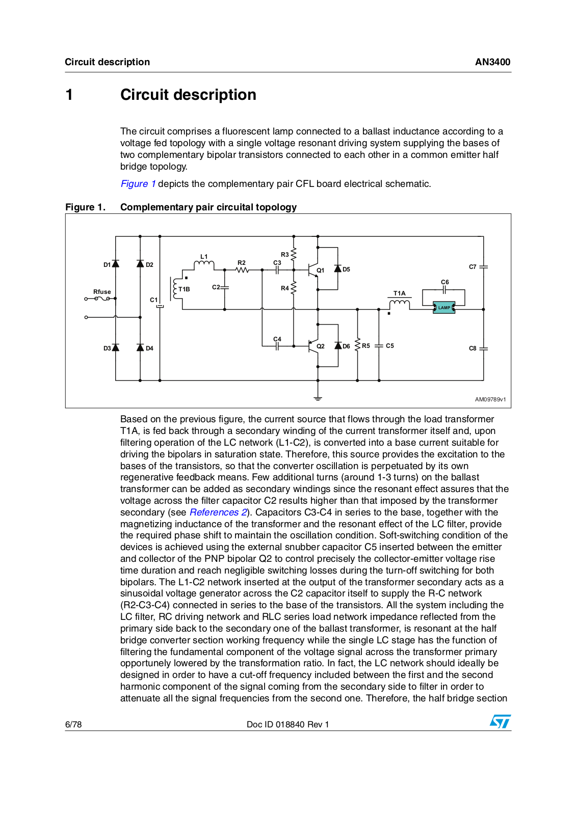
ST AN3400 Application note

AN3400

Application note

Analysis and simulation of a BJT complementary pair in a self-oscillating CFL solution

Introduction

The steady-state oscillation of a novel zero-voltages switching (ZVS) clamped-voltage (CV) self-oscillating resonant driving system for compact fluorescent lamps (CFL), using a complementary pair of bipolar transistors on the half bridge converter section, is analyzed and simulated.

One or more auxiliary windings are added on the ballast inductor in series with the lamp in order to generate the periodic signal to supply the bases of the two complementary devices connected to each other in a common emitter half bridge topology. In fact, an LC network filters, with a resonant effect, the voltage generated by the secondary winding of the load transformer, producing a novel, periodic switching signal to accurately control the bases of the transistors. The two bipolars are supplied by a unitary control signal so it is not possible to turn on both devices at once because of their opposing base-emitter junction thresholds.

Self-oscillating operation is divided into eight stages according to the variation over a period of the driving voltage signal across the filter capacitor at the output of the transformer secondary windings. Stage-wise circuit analysis shows as the resonant filter action limits the lamp current and dominates the switching frequency of the ballast in steady-state working condition.

The half bridge of the power active devices generates a rectangular voltage waveform that drives an opportunely tuned output circuit composed of a parallel loaded RLC output circuit of which the R is the steady-state LAMP resistance. For the inverter self-oscillating condition, the switching frequency is determined by all of the circuit elements related to the oscillation frequency, such as the resonant tank, gas-discharge lamp, driving circuit, and switching devices. Depending on the circuit design, its oscillation frequency is typically around 35 to 48 kHz and can be eventually increased by shortening the storage time of the bipolars. Cost benefits are achieved by the proposed self-oscillating solution that allows to drive the CFL lamp eliminating the saturable core auxiliary transformer, placed in the more traditional standard solution, without sacrificing the performance or reducing the expected life time of the lamps.

In this paper, general structure and self-oscillating principle are discussed and verified by laboratory experiment, while analytical results are validated by mathematical simulation using the Matlab tool.

November 2011

Doc ID 018840 Rev 1

1/78

www.st.com

Contents

AN3400


Contents

1

Circuit description . . . . . . . . . . . . . . . . . . . . . . . . . . . . . . . . . . . . . . . . . .

. 6

2

Startup phase . . . . . . . . . . . . . . . . . . . . . . . . . . . . . . . . . . . . . . . . . . . . . .

8

3

Bipolar transistor operating modes . . . . . . . . . . . . . . . . . . . . . . . . . . . .

9

4

Principle of self-oscillating operation . . . . . . . . . . . . . . . . . . . . . . . . . .

11

5

Steady-state stage-wise circuit analysis . . . . . . . . . . . . . . . . . . . . . . . .

15

6

Driving network modeling . . . . . . . . . . . . . . . . . . . . . . . . . . . . . . . . . . .

31

7

NPN conduction phase modeling . . . . . . . . . . . . . . . . . . . . . . . . . . . . .

36

8

Modeling of re-circulating phase preliminary to the NPN conduction


time phase . . . . . . . . . . . . . . . . . . . . . . . . . . . . . . . . . . . . . . . . . . . . . . . .

37

9

NPN storage time phase modeling . . . . . . . . . . . . . . . . . . . . . . . . . . . .

40

10

Modeling of the dead time after the NPN storage time phase . . . . . .

45

11

Modeling of the re-circulating phase preliminary to the PNP conduction


time phase . . . . . . . . . . . . . . . . . . . . . . . . . . . . . . . . . . . . . . . . . . . . . . . .

47

12

PNP conduction phase modeling . . . . . . . . . . . . . . . . . . . . . . . . . . . . .

50

13

PNP storage time phase modeling . . . . . . . . . . . . . . . . . . . . . . . . . . . .

52

14

Modeling of the dead time after the PNP storage time phase . . . . . . .

55

15

Experimental results . . . . . . . . . . . . . . . . . . . . . . . . . . . . . . . . . . . . . . . .

57


15.1

Applicative parameters . . . . . . . . . . . . . . . . . . . . . . . . . . . . . . . . . . . . . . .

57

16

Simulation results with the Matlab tool . . . . . . . . . . . . . . . . . . . . . . . . .

62


16.1

Simulative parameters . . . . . . . . . . . . . . . . . . . . . . . . . . . . . . . . . . . . . . .

62

2/78

Doc ID 018840 Rev 1

AN3400

Contents


17 Conclusions . . . . . . . . . . . . . . . . . . . . . . . . . . . . . . . . . . . . . . . . . . . . . . . 75

18 References . . . . . . . . . . . . . . . . . . . . . . . . . . . . . . . . . . . . . . . . . . . . . . . . 76

19 Revision history . . . . . . . . . . . . . . . . . . . . . . . . . . . . . . . . . . . . . . . . . . . 77

Doc ID 018840 Rev 1

3/78

List of figures

AN3400


List of figures

Figure 1.

Complementary pair circuital topology . . . . . . . . . . . . . . . . . . . . . . . . . . . . . . . . . . . . . . . .

. 6

Figure 2.

Steady-state waveforms: filter capacitor voltage signal (V(t)), NPN base current (Ibnpn)


and PNP base current (Ibpnp) . . . . . . . . . . . . . . . . . . . . . . . . . . . . . . . . . . . . . . . . . . . . . .

11

Figure 3.

Steady-state waveforms: filter capacitor voltage signal (V(t)), NPN collector current (ICnpn)


and PNP collector current (ICpnp). . . . . . . . . . . . . . . . . . . . . . . . . . . . . . . . . . . . . . . . . . .

12

Figure 4.

Steady-state waveforms: filter capacitor voltage signal (V(t)), NPN collector-emitter voltage


(VCEnpn) and PNP emitter-collector voltage (VECpnp) . . . . . . . . . . . . . . . . . . . . . . . . . .

12

Figure 5.

Steady-state waveforms: filter capacitor voltage signal (V(t)), NPN base-emitter voltage


(VBEnpn) and PNP emitter-base voltage(VEBpnp) . . . . . . . . . . . . . . . . . . . . . . . . . . . . . .

13

Figure 6.

Steady-state waveforms: filter capacitor voltage signal (V(t)), NPN base series capacitor


voltage (VCnpn) and PNP base series capacitor voltage (VCpnp). . . . . . . . . . . . . . . . . . .

13

Figure 7.

First stage: first re-circulating phase before the NPN conduction time . . . . . . . . . . . . . . . .

15

Figure 8.

First stage: second re-circulating phase before the NPN conduction time . . . . . . . . . . . . .

17

Figure 9.

Second stage: NPN conduction phase with filter capacitor charge . . . . . . . . . . . . . . . . . .

18

Figure 10.

Second stage: NPN conduction phase with filter capacitor discharge . . . . . . . . . . . . . . . .

18

Figure 11.

Third stage: NPN storage phase . . . . . . . . . . . . . . . . . . . . . . . . . . . . . . . . . . . . . . . . . . . .

20

Figure 12.

Fourth stage: dead time after NPN conduction phase . . . . . . . . . . . . . . . . . . . . . . . . . . . .

21

Figure 13.

Fifth stage: first re-circulating phase before the PNP conduction time . . . . . . . . . . . . . . . .

22

Figure 14.

Fifth stage: first re-circulating phase before PNP conduction time with PNP device working


in reverse active region. . . . . . . . . . . . . . . . . . . . . . . . . . . . . . . . . . . . . . . . . . . . . . . . . . . .

23

Figure 15.

Fifth stage: second re-circulating phase before the PNP conduction time . . . . . . . . . . . . .

24

Figure 16.

Sixth stage: PNP conduction phase with filter capacitor charge. . . . . . . . . . . . . . . . . . . . .

26

Figure 17.

Sixth stage: PNP conduction phase with filter capacitor discharge . . . . . . . . . . . . . . . . . .

26

Figure 18.

Seventh stage: PNP storage phase . . . . . . . . . . . . . . . . . . . . . . . . . . . . . . . . . . . . . . . . . .

28

Figure 19.

Eighth stage: dead time phase after PNP conduction . . . . . . . . . . . . . . . . . . . . . . . . . . . .

29

Figure 20.

Driving network modeling for the NPN bipolar conduction phase simulation . . . . . . . . . . .

31

Figure 21.

Driving network modeling for the simulation of the first re-circulating phase preliminary to


the NPN bipolar conduction time phase . . . . . . . . . . . . . . . . . . . . . . . . . . . . . . . . . . . . . . .

37

Figure 22.

Driving network modeling for the simulation of the second re-circulating phase preliminary to


the NPN bipolar conduction time phase . . . . . . . . . . . . . . . . . . . . . . . . . . . . . . . . . . . . . . .

38

Figure 23.

Driving network modeling for the NPN bipolar storage time phase simulation . . . . . . . . . .

40

Figure 24.

Variability of the extractive current negative peak IBnpn-off versus variability of the integer


n with storage time fixed . . . . . . . . . . . . . . . . . . . . . . . . . . . . . . . . . . . . . . . . . . . . . . . . . . .

41

Figure 25. Driving network modeling for the simulation of the dead time phase after the NPN bipolar


storage time phase . . . . . . . . . . . . . . . . . . . . . . . . . . . . . . . . . . . . . . . . . . . . . . . . . . . . . .

45

Figure 26.

Driving network modeling for the simulation of the first re-circulating phase preliminary to the


PNP bipolar conduction time phase . . . . . . . . . . . . . . . . . . . . . . . . . . . . . . . . . . . . . . . . . .

47

Figure 27.

Driving network modeling for the simulation of the second re-circulating phase preliminary to


the PNP bipolar conduction time phase . . . . . . . . . . . . . . . . . . . . . . . . . . . . . . . . . . . . . . .

48

Figure 28.

Driving network modeling for the PNP bipolar conduction time phase simulation . . . . . . .

50

Figure 29.

Driving network modeling for the PNP bipolar storage time phase simulation . . . . . . . . . .

52

Figure 30.

Driving network modeling for the simulation of the dead time after the PNP storage time


phase . . . . . . . . . . . . . . . . . . . . . . . . . . . . . . . . . . . . . . . . . . . . . . . . . . . . . . . . . . . . . . . . .

55

Figure 31.

STX83003 (NPN) bipolar transistor during steady-state operation with 230 V input voltage:


base current (IB1), collector current (IC1), base-emitter voltage (VBE1) and collector-emitter


voltage (VCE1) signals acquired . . . . . . . . . . . . . . . . . . . . . . . . . . . . . . . . . . . . . . . . . . . . .

58

Figure 32.

STX83003 (NPN) bipolar transistor during steady-state operation with 230 V input voltage:


base current (IB1), collector current (IC1), voltage on base series capacitor Cn (VCN) and


4/78

Doc ID 018840 Rev 1

AN3400

List of figures


voltage on base series capacitor Cp (VCP) signals acquired . . . . . . . . . . . . . . . . . . . . . . . 58 Figure 33. STX83003 (NPN) bipolar transistor during steady-state operation with 230 V input voltage:

base current (IB1), collector current (IC1), voltage on filter capacitor C2 (VC) and voltage on driving resistance R2 (VRS) signals acquired. . . . . . . . . . . . . . . . . . . . . . . . . . . . . . . . . . . 59

Figure 34. STX83003 (NPN) bipolar transistor during steady-state operation with 230 V input voltage: base current (IB1), collector current (IC1), voltage on base series capacitor C3 (VCN)

and voltage on breakdown resistance R4 (VRBN) signals acquired . . . . . . . . . . . . . . . . . 59 Figure 35. STX83003 (NPN) bipolar transistor during turn-on particular in steady-state operation with

230 V input voltage: base current (IB1), collector current (IC1) and collector-emitter voltage

(VCE1) signals acquired . . . . . . . . . . . . . . . . . . . . . . . . . . . . . . . . . . . . . . . . . . . . . . . . . . . 60 Figure 36. STX83003 (NPN) bipolar transistor during turn-off particular in steady-state operation with

230 V input voltage: base current (IB1), collector current (IC1) and collector-emitter voltage

(VCE1) signals acquired . . . . . . . . . . . . . . . . . . . . . . . . . . . . . . . . . . . . . . . . . . . . . . . . . . . 60 Figure 37. STX93003 (PNP) bipolar transistor during turn-on particular in steady-state operation with

230 V input voltage: base current (IB2), collector current (IC2) and emitter-collector voltage

(VCE2) signals acquired . . . . . . . . . . . . . . . . . . . . . . . . . . . . . . . . . . . . . . . . . . . . . . . . . . . 61 Figure 38. STX93003 (PNP) bipolar transistor during turn-off particular in steady-state operation with

230 V input voltage: base current (IB2), collector current (IC2) and emitter-collector voltage

(VCE2) signals acquired . . . . . . . . . . . . . . . . . . . . . . . . . . . . . . . . . . . . . . . . . . . . . . . . . . . 61 Figure 39. Current source signal Is modeling for the simulation on the re-circulating phase before the

NPN conduction phase . . . . . . . . . . . . . . . . . . . . . . . . . . . . . . . . . . . . . . . . . . . . . . . . . . . . 63 Figure 40. Re-circulating phase preliminary to the NPN conduction time phase . . . . . . . . . . . . . . . . . 65 Figure 41. NPN conduction time phase . . . . . . . . . . . . . . . . . . . . . . . . . . . . . . . . . . . . . . . . . . . . . . . . 66 Figure 42. NPN storage time phase. . . . . . . . . . . . . . . . . . . . . . . . . . . . . . . . . . . . . . . . . . . . . . . . . . . 67 Figure 43. Dead time phase after the NPN storage time phase . . . . . . . . . . . . . . . . . . . . . . . . . . . . . 68 Figure 44. Re-circulating phase preliminary to the PNP conduction time phase . . . . . . . . . . . . . . . . . 69 Figure 45. PNP conduction time phase . . . . . . . . . . . . . . . . . . . . . . . . . . . . . . . . . . . . . . . . . . . . . . . . 70 Figure 46. PNP storage time phase. . . . . . . . . . . . . . . . . . . . . . . . . . . . . . . . . . . . . . . . . . . . . . . . . . . 71 Figure 47. Dead time phase after the PNP storage time phase . . . . . . . . . . . . . . . . . . . . . . . . . . . . . 72 Figure 48. Driving network simulation results: filter capacitor voltage signal (Vs), NPN base series

capacitor voltage (VCn) and PNP base series capacitor voltage (VCp) signals simulated . 73 Figure 49. Driving network simulation results: NPN base current (Ibn) and PNP base current (Ibp)

signals simulated . . . . . . . . . . . . . . . . . . . . . . . . . . . . . . . . . . . . . . . . . . . . . . . . . . . . . . . . 74 Figure 50. Driving network simulation results: NPN base series capacitor current (ICn) and PNP base

series capacitor current (ICp) signals simulated . . . . . . . . . . . . . . . . . . . . . . . . . . . . . . . . . 74

Doc ID 018840 Rev 1

5/78

Circuit description

AN3400


1 Circuit description

The circuit comprises a fluorescent lamp connected to a ballast inductance according to a voltage fed topology with a single voltage resonant driving system supplying the bases of two complementary bipolar transistors connected to each other in a common emitter half bridge topology.

Figure 1 depicts the complementary pair CFL board electrical schematic.

Figure 1. Complementary pair circuital topology


L1

R3


D1

D2

R2

C3

D5


C7


Q1


T1B

C2

R4


C6

Rfuse


T1A

C1


LAMP


C4


R5

C5


D3

D4


Q2

D6

C8


AM09789v1

Based on the previous figure, the current source that flows through the load transformer T1A, is fed back through a secondary winding of the current transformer itself and, upon filtering operation of the LC network (L1-C2), is converted into a base current suitable for driving the bipolars in saturation state. Therefore, this source provides the excitation to the bases of the transistors, so that the converter oscillation is perpetuated by its own regenerative feedback means. Few additional turns (around 1-3 turns) on the ballast transformer can be added as secondary windings since the resonant effect assures that the voltage across the filter capacitor C2 results higher than that imposed by the transformer secondary (see References 2). Capacitors C3-C4 in series to the base, together with the magnetizing inductance of the transformer and the resonant effect of the LC filter, provide the required phase shift to maintain the oscillation condition. Soft-switching condition of the devices is achieved using the external snubber capacitor C5 inserted between the emitter and collector of the PNP bipolar Q2 to control precisely the collector-emitter voltage rise time duration and reach negligible switching losses during the turn-off switching for both bipolars. The L1-C2 network inserted at the output of the transformer secondary acts as a sinusoidal voltage generator across the C2 capacitor itself to supply the R-C network (R2-C3-C4) connected in series to the base of the transistors. All the system including the LC filter, RC driving network and RLC series load network impedance reflected from the primary side back to the secondary one of the ballast transformer, is resonant at the half bridge converter section working frequency while the single LC stage has the function of filtering the fundamental component of the voltage signal across the transformer primary opportunely lowered by the transformation ratio. In fact, the LC network should ideally be designed in order to have a cut-off frequency included between the first and the second harmonic component of the signal coming from the secondary side to filter in order to attenuate all the signal frequencies from the second one. Therefore, the half bridge section

6/78

Doc ID 018840 Rev 1

AN3400

Circuit description


working frequency and, consequently, the lamp power are influenced by the sizing of both L1 and C2 components. Capacitor C2 has also the function of putting the base current in phase with the collector current. Resistance R2 of the series R-C network has the function of regulating the current level to provide to the bases of both transistors acting on the power lamp. In the proposed driving solution, the two capacitors C3 and C4 are charged with opposite polarity to each other and assuming the same polarity of the base-emitter voltage of the relevant bipolar transistor. In the regular functionality, when a capacitor goes through a charging phase, before or during the conduction time of the relevant bipolar, so the opposite capacitor is discharging contemporarily with a long constant time due to the series with the breakdown resistance R4. So, this resistance R4, inserted between the bases of the two transistors, creating an alternative path for the discharge of each capacitor, also avoids that the oscillation is blocked during startup phase when one of the two capacitors is fully charged. Regulating the discharge time of each capacitor, this resistance allows to fine tune the working frequency and consequently the power supplied to the lamp. Two capacitors C3 and C4 are not totally discharged during a forcing voltage source period but maintain always a residual charge passing from the discharging to the charging transient. Therefore, current across the breakdown resistance R4 flows always in the same direction going from the PNP to the NPN base because the two capacitors maintain always the same polarity during a period of the voltage signal across the C2 filter capacitor. A breakdown resistance with a too high value can increase the working frequency but also can bring the reverse biased base-emitter junction of the inactive device in breakdown condition. And vice versa, a too low value of the breakdown resistance could cause re-conduction peaks in the PNP transistor at the high temperature when the emitter-collector voltage reaches the maximum value. In particular only the PNP device can show the phenomena above mentioned because it has a lower base-emitter breakdown voltage and it has a higher low

current hfe than the NPN one. Setting the resistance R4 in order to guarantee a VBEoff value in the range -4 V to -7 V, it is possible to avoid breakdown phenomena for the base-emitter

junctions of the bipolars and, at the same time, anomalous re-conduction effects due to unexpected disturbances.

Doc ID 018840 Rev 1

7/78

Startup phase

AN3400


2 Startup phase

The two bipolar transistors should have an appropriately high gain value in order to guarantee the correct ignition of the lamp during the startup phase. Compact fluorescent lamps usually require about 600 V as peak voltage to strike the arc. Once the arc is established about 100 V are enough to sustain it while, electrically, the resistance of the lamp falls from about one mega ohm down to a few hundred ohm (see References 1). Furthermore, the value of the load inductance L of the ballast must be chosen so that it does not saturate at the operative current of the lamp, even at high temperatures. In fact the lamp is ignited by generating an overvoltage across the capacitor C6 in parallel to the tube, through the circuit formed by the series of the ballast transformer primary inductance and C6-C7-C8 capacitors. At startup the lamp is an open circuit and the C6 capacitor imposes the resonant frequency of the circuit as C6 is much smaller than the C7-C8 ones. The imposed overvoltage is high enough to ionize almost instantaneously the gas in the lamp. Once the lamp is lighted, the capacitor C6 is short-circuited by the lamp itself and the natural frequency is determined mainly by the capacitors C7-C8 charged/discharged through the DC-AC converter. The startup network is represented by the only resistor R3, connected between the collector and the base of the high side transistor, since the capacitors in series with the bases act as a high impedance elements during the first instant of the startup.

8/78

Doc ID 018840 Rev 1

AN3400

Bipolar transistor operating modes


3 Bipolar transistor operating modes

Bipolars switching in the resonant circuit have three different operating modes in normal working conditions: re-circulating, conduction and transition phases.

During the re-circulating phase, the transistor isn't yet in conduction state and passes from a first inactive state in which its B-C junction diode is activated to allow the re-circulation of load inductor demagnetization current ILP shared with the external diode in anti-parallel to the device itself, to a second inactive state in which the external diode is turned off but both of the two B-E and B-C junctions are forward biased in order to complete the residual demagnetization of the Lp inductor until the forcing re-circulating current ILP, that imposes the negative collector current, reaches the zero value. In conduction mode, the two B-E and B-C junctions of the transistor continue to be forward biased and the bipolar transistor conducts a positive magnetization current for the inductive load. The turn-off mechanism occurs in three stages: “storage time”, or time spent to extract the storage in excess and recombine the charge stored on the base, “current fall time”, in which the collector current passes from 90% to 10% of its maximum value, and “rise time” of the collector-emitter voltage. The transition mode occurs during the voltage rise time and represents a sort of “dead time” phase in which both bipolars are substantially inactive since only the B-C and B-E junction capacitances of both devices are interested in being charged/discharged in reverse bias. This phase anticipates the re-circulating phase preliminary to the conduction phase of the complementary device. During the turn-off process, the dynamic operation point of the transistor moves through three different operating regions on the current-voltage IC-VCE characteristic: “hard saturation region”, “quasi saturation region” and “active region”.

Hard saturation region: at the first instance of turn-off switching time, the base-collector junction is forward biased and the base region and collector drift region are both in high-level injection condition. An excess carrier distribution fills the collector drift region and the storage time is just the time required to remove/extract this charge stored in excess. Also the contribution of charge decay due to recombination, depending on the minority-carrier lifetime, influences this phase. During the storage time process the

base-emitter voltage does not change immediately from its forward bias value VBESAT, due to the excess minority carriers stored in the base region, and also the collector-emitter voltage remains constant. The extent of storage time is dependent not only on the amount of excess charges remaining in the collector drift region but also on the external driving. Excess minority carriers are removed from the base region and base-collector junction at a constant rate determined by the negative base drive voltage, as well as the base drive resistance, and proportional to the reverse base

current IBoff slope. So the excess charge at the base-collector junction begins to reduce due to charge removal to make up for the reverse base current and the collector current continues to increase.

Quasi saturation region: after the storage time, the forward biased base-collector junction is out of high-level injection and the remaining charges stored in the base become insufficient to support the transistor in the hard saturation region. Therefore, at this point the transistor enters quasi saturation region in which the depletion region begins to expand while a voltage appears across it and the collector-emitter voltage starts rising with a small slope. After having removed the charges in the drift region holding the bipolar in the quasi saturation region, the transistor enters the active region.

Active region: crossing the active region, the charges stored in the base region are insufficient to support the full negative base current so the base-emitter voltage starts falling negatively and the negative base current starts reducing. Correspondingly, the stored base charges can no longer support the full load current through the collector so that also the collector current decays exponentially resulting in current fall time required

Doc ID 018840 Rev 1

9/78

Bipolar transistor operating modes

AN3400


to remove remaining stored charge in base. Both of the slopes dictated by base current and collector current simultaneously decay with time due to recombination.

Collector-emitter voltage increases rapidly towards the rectified voltage upper rail VCC until it is exceeded in order to turn-on the anti-parallel diode of the complementary device at the end of the rise time interval. The increasing voltage is supported across the collector drift region while the expanding depletion region at the base-collector junction sweeps out the excess charge until it totally sustains the bus voltage.

To reduce the stress on the devices, and hence the switching losses, the half bridge converter switches under zero voltage (ZVS) conditions, in which turn-on losses are absent and a favorable turn-off trajectory of power transistors can be ensured by the use of a snubber capacitor. In fact, contrary to the hard switching dynamic, in which the voltage rise was a function of the amount of charge in the drift region after the storage phase, with the soft-switching dynamic the rate of voltage rise during turn-off is controlled by the snubber capacitor connected across the device. While the voltage continues to raise, the collector current decays to zero and the load current flows into the snubber capacitor until the device voltage reaches the bus voltage. Therefore, even though turn-off does not occur at exactly zero volts, the stresses on the device are much reduced compared to hard-switching mode. When the collector current reaches the zero value, the bipolar turn-off process is completed and the load current starts to freewheel through the anti-parallel diode of the complementary device.

10/78

Doc ID 018840 Rev 1

AN3400

Principle of self-oscillating operation


4 Principle of self-oscillating operation

The current through the transformer primary T1A and the resonant network at the half bridge output consists of two portions of waveforms, one when the load inductor is clamped to the upper rail at the end in common with the emitter node of the bipolars by the NPN bipolar Q1 and its anti parallel diode D5, and the other one when it is clamped by the PNP bipolar Q2 and its anti parallel diode D6 to the lower rail. The intervals, when the snubber capacitor C5 is charging/discharging while the emitter common node ramps between the rails, are generally short compared to the conduction periods. To achieve the ZVS working condition, the bipolar transistor is turned on at the end of the re-circulating phase of the residual demagnetization current from the load transformer.

Figure 2, 3, 4, 5 and 6, describe the main conceptual steady-state signals related to the theoretical working principle of the proposed driving system.

These figures highlight the different operating phases of the two complementary bipolar transistors during the steady-state normal working conditions:

Re-circulating time phases with a time length of “tA” and “tC” respectively for the NPN and PNP transistors

Conduction time phases indicated with “NPN-IBontime” and “PNP-IBontime

Storage time phases indicated with “NPN-IBstoragetime” and “PNP-IBstoragetime

Dead time phases with the time length of “tB” and “tD” respectively for the NPN and PNP transistors.

As previously described, the “dead time phase” refers to the transient occurring during the voltage rise time and in which both of the bipolars are substantially inactive since only the B-E and B-C junction capacitances on both devices are interested in being charged/discharged in reverse bias. Moreover, from this point on and for the whole steady-state analysis subsequently explained, it is assumed to name, for the sake of simplicity, as storage time the interval including both the effective storage time and fall time of the device.

Figure 2. Steady-state waveforms: filter capacitor voltage signal (V(t)), NPN base current (Ibnpn) and PNP base current (Ibpnp)

AM09793v1

Doc ID 018840 Rev 1

11/78

ST AN3400 Application note

Principle of self-oscillating operation

AN3400


Figure 3. Steady-state waveforms: filter capacitor voltage signal (V(t)), NPN collector current (ICnpn) and PNP collector current (ICpnp)

AM09794v1

Figure 4. Steady-state waveforms: filter capacitor voltage signal (V(t)), NPN collector-emitter voltage (VCEnpn) and PNP emitter-collector voltage (VECpnp)

AM09795v1

12/78

Doc ID 018840 Rev 1

AN3400

Principle of self-oscillating operation


Figure 5. Steady-state waveforms: filter capacitor voltage signal (V(t)),

NPN base-emitter voltage (VBEnpn) and PNP emitter-base voltage(VEBpnp)

AM09796v1

Figure 6. Steady-state waveforms: filter capacitor voltage signal (V(t)), NPN base series capacitor voltage (VCnpn) and PNP base series capacitor voltage (VCpnp)

AM09797v1

In Figure 2 the filter capacitor voltage V(t) and the base currents Ibnpn and Ibpnp of the two bipolars during a period of the voltage signal filtered are shown. Two different signal

thresholds fix respectively the turn-on and turn-off instants of the devices during their working operation period. In particular, in the previous figure it is evident that, starting from the driving source voltage, the turn-on of the NPN transistor is possible only when the V(t) is

higher than the VCnpnon-char+VBEsatnpn value and similarly the turn-on of the PNP transistor is possible only when the V(t) is lower than the -VCpnpon-char-VEBsatpnp value. On the contrary, the turn-off of the NPN transistor is possible only when the V(t) is lower than the

VCnpnon-dischar+VBEsatnpn value and, similarly, the turn-off of the PNP transistor is possible only when the V(t) is higher than the -VCpnpon-dischar-VEBsatpnp value.

Figure 3 shows the filter capacitor voltage V(t) and the collector currents ICnpn and ICpnp of the two bipolars during a period of the voltage signal filtered. It can be seen as the collector currents pass through the zero value at the end of the re-circulating phases in which the whole residual external demagnetization current, imposed by the load inductor, has

Doc ID 018840 Rev 1

13/78

Principle of self-oscillating operation

AN3400


elapsed. Instants of turn-on switching are at t2 (or t14) and t8 times respectively for the NPN and PNP devices.

Figure 4 shows the filter capacitor voltage V(t) and the collector-emitter voltage VCEnpn signal and emitter-collector voltage signal VECpnp respectively of the NPN and PNP bipolars during a period of the voltage signal filtered. In this image the waveforms are not reported in

scale since the voltage signals VCEnpn and VECpnp assume far higher levels compared to the V(t) signal ones.

Figure 5 shows the filter capacitor voltage V(t) and base-emitter voltage signal VBEnpn and emitter-base voltage signal VEBpnp respectively of the NPN and PNP bipolars during a

period of the voltage signal filtered.

Figure 6 shows the filter capacitor voltage V(t) and the voltage signals across the capacitors

VCnpn and VCpnp in series, respectively, to the bases of the NPN and PNP bipolars during a period of the voltage signal filtered. It is possible to see as the different signal thresholds

impose the initial instants of the charging and discharging phases for the capacitors in series to the bases.

Observing the waveforms attached, which describe the resonant driving functionality, it is clearly possible to distinguish the different working operation phases of the two devices

during a switching period. In particular, when V(t)>V


+V

with

d

(V(t))> 0

,

Cnpnon-char


BEsatnpn


dt


NPN conduction time begins and when V(t) decreasing positively reaches the

VCnpnon-dischar+VBEsatnpn value (that is V(t)<VCnpnon-dischar+VBEsatnpn with

d (V(t))< 0 ), the NPN storage time phase starts. After the fall time period, NPN bipolar can

dt

no longer sustain its collector current so the voltage of the midpoint in common with the PNP emitter changes. At this time, the short transition mode ('dead time' after the NPN

conduction time has elapsed) begins (for 0<V(t)<VCnpnoff-char+VBEsatnpn with

d (V(t))< 0 ), where both bipolars are off and the snubber capacitance carries the load

dt

resonant inductor current while the B-C junction capacitances of the devices are respectively charged (NPN) and discharged (PNP). Similarly, when

V(t)<-V

Cpnpon-char

-V

EBsatpnp

with

d

(V(t))< 0 , PNP conduction time begins and when

dt


decreasing V(t), in module, negatively reaches the -VCpnpon-dischar-VEBsatpnp value (that is

V(t)>-V


-V


with

d

(V(t))> 0 ), the PNP storage time phase starts.

Cpnpon-dischar

EBsatpnp


dt

Short transition mode after the PNP conduction time ('dead time' after the PNP conduction time has elapsed) begins when -VCpnpoff-char-VEBsatpnp<V(t)<0 with

d (V(t))> 0 in which the B-C junction capacitances of the PNP and NPN devices are dt

respectively charged and discharged. Re-circulating phases elapse respectively for

0<V(t)<V


+V


and

d

(V(t))> 0

with the NPN device turned on at t


(or t

)

Cnpnon-char

BEsatnpn


2


dt


d


14

instant and for -V

Cpnpon-char

-V


<V(t)<0 and

(V(t))< 0 with the PNP device turned on

at t8 instant.

EBsatpnp


dt


14/78

Doc ID 018840 Rev 1

AN3400

Steady-state stage-wise circuit analysis


5 Steady-state stage-wise circuit analysis

This section provides a comprehensive description of the resonant filter working operation using a stage-wise circuit analysis divided into eight phases in accordance with the variation over a period of the voltage signal across the filter capacitor V(t) at the output of the transformer secondary windings. The dynamic behavior of the resonant driving system can be easily described by applying, in the time domain, Kirchhoff's voltage law on the loops containing the filter capacitor C2 and the R-C network (R2-R4-C3-C4) connected in series to the bases of the transistors and Kirchhoff's current law on the nodes with the branches of the base series capacitors connected to it. The mathematical model developed is useful for the successive simulation in Matlab environment.

Stage 1: t0<t<t2 and t12<t<t14: (re-circulating phase before the NPN conduction time:

0<V(t)< V

Cnpnon-char

+V

BEsatnpn

with

d

(V(t))> 0 )


dt

The re-circulating phase is referred to all the demagnetization transient of the load inductor Lp elapsing until its current ILP reaches the zero value at the end of this stage. This phase, in which both Q1-Q2 switches are inactive, can be subdivided into a further two sub-phases distinguished by the following:

First re-circulating phase before the NPN conduction time (t0<t<t1 and t12<t<t13): Both Q1-Q2 switches are turned off and the anti-parallel diode D1 of the NPN transistor conducts, sharing with the forward biased B-C NPN bipolar junction, the

residual demagnetization current ILP from the load inductor Lp. Voltage across the filter capacitor C increases and charges the capacitor Cn in series to the not yet forward biased NPN base-emitter junction, therefore assuming the same polarity

of the relevant VBEnpn-on, whereas the capacitor Cp begins to discharge through the breakdown resistance Rb. In this re-circulating stage, currents and voltages on the driving network are represented by the information in Figure 7.

Figure 7. First stage: first re-circulating phase before the NPN conduction time

NPN base-collector diode conduction

VDD


L

VRs

VCn


VBCn


IRs

ICn


IBCn


Rs

Cn


VBEn

Ls


c

VC

Rb


VRb


IRb

First re-circulating phase

Cp


VBEp

before NPN conduction


ICp

VCp

D1

Q1

VD1

ID1

ILP

Lp

D2

Q2 Cs VCs

GND

AM09798v1

Doc ID 018840 Rev 1

15/78

Steady-state stage-wise circuit analysis

AN3400


According to the agreement in Figure 7, the following equations are valid in the driving section during the first re-circulating stage for t0<t<t1 and t12<t<t13:

System of equations 1


V(t)= VC (t)


VBEn (t)= VBCn (t)− VD1(t)< VBEn−on where VBCn (t)> VBCn−on and VD1 (t)> VD1−on

VCn (t)= VCnor1a +

1


t1

(t)dt


VCnor1a = VCn (t0− )


t0 ICn

where

C


n


1


t1


VCp (t)= VCpor1a


t0ICp

(t)dt

where

VCpor1a = VCp (t 0− )

Cp

I


(t)= C


d

(V (t))


dt


Cn


n


Cn


ICp (t)= −Cp d (VCp (t))

dt

IBCn (t)=ICn (t)+ICp (t)=ILP (t)−ID1(t)= IRS (t)

VCn (t)+ VCp (t)= VRb (t)= VBEp (t)− VBEn (t) with VBEp (t)= −VEBp (t)> 0

in which IBCn and VBCn are, respectively, the current signal and voltage signal of the NPN bipolar forward conducting B-C junction diode. During this phase, in general, VBEn(t) voltage

is so that 0<VBEn(t)<VBEn-on for the NPN bipolar B-E junction diode, but if it were VBEn(t)<0 the device would work in reverse active region as it is VBCn(t)>0.

Neglecting the reverse recovery time of the anti-parallel diode D1, the subsequent phase is given by the following second re-circulating phase before the NPN conduction time.

Second re-circulating phase before the NPN conduction time (t1<t<t2 and t13<t<t14):

In this phase the NPN bipolar transistor acts as two uncoupled/independent diodes. In fact, the external diode D1 is turned off and the NPN device continues to be inactive but, contrary to the previous first re-circulating phase, both of its two B-E and B-C junctions are forward biased in order to complete the residual demagnetization of the Lp inductor until the forcing re-circulating current ILP, that imposes the negative (extractive) collector current, reaches the zero value. Voltage across the filter capacitor C continues to increase and charge the capacitor Cn in series to the forward biased NPN base-emitter junction whereas the capacitor Cp continues to discharge through the breakdown resistance Rb. When the inductive resonant current reverses, after t2 instant, the successive phase starts and the NPN device Q1 conducts carrying a positive (coming in) collector current ICnpn. In this second re-circulating stage, currents and voltages on the driving network are represented by the information in Figure 8.

16/78

Doc ID 018840 Rev 1

AN3400

Steady-state stage-wise circuit analysis


Figure 8.

First stage: second re-circulating phase before the NPN conduction time


NPN base-collector diode conduction

VDD


ICnpn

L

VRs

VCn


VBCn

D1

IRs

ICn


IBnpn

Rs

Cn


Q1


Ls

c

VC

VBEn


Rb

IEnpn


VRb

ILP


Lp


IRb


NPN base-emitter


diode conduction

Cp

Second re-circulating phase

ICp

before NPN conduction

VCp

VBEp

D2

Q2 Cs VCs

GND

AM09799v1

According to the agreement of the previous image, the following equations are valid in the driving section during the second re-circulating stage for t1<t<t2 and t13<t<t14:

System of equations 2


V(t)= VC (t)


VBEn (t)= VBEn−on


VBCn (t)= VBCn−on and VECn (t)= −VCEn (t)< VD1−on


(t)= V

+

1


t2


(t)dt

where


= V t

V


I


V


Cn


Cn

Cnor1b


t1

Cn


Cnor1b

Cn (1−)

VCp (t)= VCpor1b

1


t2


(t)dt

where VCpor1b = VCp (t1− )

t1ICp

C


p


I


(t)= C

d

(V (t))


Cn


n dt

Cn


ICp (t)= −Cp d (VCp (t))

dt

IBnpn (t)=ICn(t)+ICp(t)= ICnpn(t)+IEnpn(t)= ILP(t)+IEnpn (t)=IRS(t)

VCn (t)+ VCp (t)= VRb (t)= VBEp (t)−VBEn (t) with VBEp (t)= −VEBp (t)> 0

Stage 2: t2<t<t4: (NPN conduction time: V(t)>VCnpnon-char+VBEsatnpn during filter

capacitor C charging phase for t2<t<t3 with d (V(t))> 0 and dt

V(t)>VCnpnon-dischar+VBEsatnpn during filter capacitor C discharging phase for t3<t<t4

with d (V(t))< 0 ). dt

From the t2 instant V(t) voltage is higher than the VCnpnon-char+VBEsatnpn value and increases up to reach its maximum value at t3. NPN transistor Q1 is turned on under

zero voltage switching (ZVS) and the current in the resonant load inductor increases. Capacitor Cn continues to be charged up by the source V(t), whereas capacitor Cp discharges through the breakdown resistance Rb inserted between the bases of the

Doc ID 018840 Rev 1

17/78

Steady-state stage-wise circuit analysis

AN3400


two transistors. After t3 instant voltage across the filter capacitor C decreases from its maximum value while the capacitor Cn continues to charge until it reaches its maximum value and the capacitor Cp to discharge maintaining a share of conduction current on the base IBn of the NPN bipolar Q1. During this stage, the base current IBn is the superposition of two components, one generated by the Cn charging transient and the other one generated by the Cp discharging transient through the breakdown resistance Rb. In this way, it is possible to see the voltage signal VCp, as a voltage source when the NPN device Q1 is conducting. In this stage, currents and voltages on the driving network are represented by the information in Figure 9 and 10.

Figure 9. Second stage: NPN conduction phase with filter capacitor charge


L

VRs

VCn


IRs

ICn


Rs

Cn

Ls


c


VC


Rb


Filter capacitor charge

VDD

ICnpn

IBnpn

VCEn

Q1


VBEn

D1


IEnpn

VRb

ILP


Lp

IRb


Cp

NPN conduction phase

ICp

VCp

VBEp


D2

VCs

Q2

Cs

GND

AM09800v1

Figure 10. Second stage: NPN conduction phase with filter capacitor discharge


L

VRs

VCn


IRs

ICn


Rs

Cn

Ls


c


VC


Rb


Filter capacitor discharge

VDD

ICnpn

IBnpn

VCEn

Q1


VBEn

D1


IEnpn

VRb

ILP


Lp

IRb


NPN conduction phase

Cp


ICp


VCp

VBEp


D2

VCs

Q2

Cs

GND

AM09801v1

18/78

Doc ID 018840 Rev 1

AN3400

Steady-state stage-wise circuit analysis


According to the agreement of the previous images, the following equations are valid in the driving section during the NPN conduction stage for t2<t<t4:

System of equations 3

V (t)=VC (t)

VBEn (t)=VBEnsat

VCEn (t)=VCEnsat

VCn (t)=VCnoc1 + 1

Cn

VCp (t )= VCpoc1 1

Cp

tt24ICn (t)dt

tt24ICp (t)dt

where VCnoc1 =VCnpnonchar =VCn (t2)

where VCpoc1 =VCp (t2 )

I

Cn

(t )= C

n


d

(V

Cn

(t))


dt


I

Cp

(t)= −C

p


d

(V

Cp

(t))


dt


I Bnpn on (t)= ICn (t)+ ICp (t)= I Enpn (t)I LP (t)= I RS (t) where ILP (t)= ICnpn (t)

VCn

(t)+VCp

(t)=VRb

(t)=VBEp (t )VBEn (t)

with VBEp (t)= −VEBp (t )> 0

VC

(t)=VRS

(t)+VCn (t )+VBEn

(t)


where VBEn-sat is the voltage of the forward conducting B-E junction diode of the NPN bipolar and IBnpn-on is the base current for the NPN bipolar working in saturation state.

Stage 3: t4<t<t5: (NPN storage time:

VCnpnoff-char+VBEsatnpn<V(t)<VCnpnon-dischar+VBEsatnpn with d (V(t))< 0 ) dt

The decreasing voltage V(t) across the filter capacitor C equals the

VCnpnon-dischar+VBEsatnpn value at t4 instant. At this point the voltage on the capacitor Cn starts to decline but the stored charges of the NPN bipolar base keep the NPN

conducting with a negative base current (extraction base current IBnpn-off) while the Cp capacitor maintains its discharging phase. After the stored excess charges have disappeared, the operating point of the NPN enters its active region and VCEnpn voltage begins to increase while the collector current ICnpn drops. Therefore, the collector

current ICnpn fall time phase is included in this state until the NPN bipolar Q1 is gradually soft switched on turn-off. In this stage, currents and voltages on the driving

network are represented by the information in Figure 11.

Doc ID 018840 Rev 1

19/78

Steady-state stage-wise circuit analysis

AN3400


Figure 11. Third stage: NPN storage phase


L

VRs

VCn


IRs

ICn


Rs

Cn

Ls

c

VC

Rb


NPN storage phase

Cp

ICp

VCp

VDD

ICnpn

VCEn

IBnpn

Q1

D1

VBEn


IEnpn

VRb

ILP

Lp

IRb

VBEp

D2

VCs

Q2

Cs

GND


AM09802v1


According to the agreement of the previous image, the following equations are valid in the driving section during the NPN storage time for t4<t<t5:

System of equations 4

V(t)= VC(t)


VBEn (t)= VBEn−sat


VCEn (t)≥ VCEn−sat


1


t5


VCn (t)= VCnos1


t4 ICn (t)dt

where VCnos1 = VCn (t4−)

C


n


VCp (t)= VCpos1

1


t5

(t)dt

where VCpos1 = VCp (t4−)


t4 ICp

C


p


ICn (t)= −Cn d (VCn (t)) dt

ICp (t)= −Cp d (VCp (t)) dt

IBnpn−off (t)= ICn (t)−ICp (t)=ILP (t)−IEnpn (t)= IRS (t) where ILP (t)= ICnpn (t)

VCn (t)+ VCp (t)= VRb (t)= VBEp (t)−VBEn (t) with VBEp (t)= −VEBp (t)> 0 VC (t)= −VRS(t)+ VCn (t)+ VBEn (t)

where IBnpn-off is the extracting base current during the storage time of the NPN bipolar. Stage 4: t5<t<t6: (dead time after the NPN conduction phase:

0<V(t)<VCnpnoff-char+VBEsatnpn with d (V(t))< 0 ) dt

At t5 instant, the load inductor current ILP continues to decay and the resonant current is commutated from the NPN bipolar Q1 to the snubber capacitor Cs that discharges. As a result, the voltage on the common emitter node of the two switches decreases linearly from the upper rail to the lower rail until the emitter voltage of the PNP transistor Q2 begins to go negative with respect to the lower rail (ground reference) at t6 and the anti-parallel diode D2 of the PNP transistor starts to conduct beginning the next fifth stage. At the end of this “dead time” stage, the voltage on the capacitor Cp is reduced

20/78

Doc ID 018840 Rev 1

AN3400

Steady-state stage-wise circuit analysis


to the minimum value whereas the voltage on the capacitor Cn keeps nearly constant. The final instant t6, from which the ICp capacitor current changes polarity, marks the change of the V(t) signal polarity and one-half of its period. In this stage, currents and voltages on the driving network are represented by the information in Figure 12, in which the charging/discharging effects of the reverse biased B-E junction capacitances, respectively, for the NPN and PNP devices, are neglected and so it is possible to

approximate IBnpn (t) ICCBn (t) and IBpnp (t) ICBCp(t).

Figure 12. Fourth stage: dead time after NPN conduction phase

NPN base-collector junction capacitance charge


L

VRs


IRs


Rs

Ls

c

VC


PNP collector-base junction capacitance discharge

Dead time phase after NPN conduction


VDD


VCn


VCCBn


VCEn


ICn


ICCBn

Q1


Cn


VEBn


D1


Rb


VRb


ILP


Lp


IRb


ICs


Cp


VBEp


D2

Cs

VCs

ICp


Q2


ICBCp


VCp


VCBCp

GND


AM09803v1

According to the agreement of the previous image, the following equations are valid in the driving section during the dead time after the NPN conduction phase for t5<t<t6:

System of equations 5

V(t)= VC (t)

VCEn(t)> VCEn−sat

VBEn(t)= VEBn(t)= −(VDD −VCCBn(t)− VCS(t))> 0 VBEn(t)< 0

VEBp (t)= VBEp(t)= VCBCp(t)− VCS(t)> 0 VEBp (t)< 0


1


t6


VCn (t)= VCnod1


t5 ICn(t)dt

where VCnod1 = VCn(t5− )

C


n


VCp(t)= VCpod1

1


t6

(t)dt

where VCpod1 = VCp(t5− )


t5 ICp

C


p


ICn (t)= −Cn d (VCn (t))

dt

ICp(t)= −Cp d (VCp (t))

dt

IRS(t)=ICCBn(t)+ICBCp (t)= ILP(t)−ICS(t)

IC S (t)= −Cs d (VCS (t))

dt

VCn (t)+ VCp(t)= VRb (t)= VBEp (t)+ VEBn (t)

VC (t)= −VRS(t)+ VCn (t)− VEBn(t)

Doc ID 018840 Rev 1

21/78

Steady-state stage-wise circuit analysis

AN3400


where ICCBn is the charging current of the NPN bipolar B-C junction capacitance and ICBCp is the discharging current of the PNP bipolar C-B junction capacitance.

Stage 5: t6<t<t8: (re-circulating phase before the PNP conduction time:

-VCpnpon-char -VEBsatpnp< V(t)<0 with d (V(t))< 0 ) dt

As done for the re-circulating phase before the NPN conduction time (t0<t<t2), this phase, in which both Q1-Q2 switches are inactive, can be subdivided into a further two sub-phases distinguished by the following:

First re-circulating phase before the PNP conduction time (t6<t<t7): both Q1-Q2 switches are turned off and the load inductor residual magnetization current ILP circulates freely through the PNP transistor anti-parallel diode D2 and the directly biased C-B junction of the PNP bipolar Q2. Voltage across the filter capacitor C increases in the opposite polarity than the NPN turn-on phase and charges the

capacitor Cp in series to the not yet forward biased base of the PNP, assuming the same polarity of the relevant VEBonpnp, while the capacitor Cn begins to decrease its charge through the breakdown resistance Rb. In this re-circulating stage, currents and voltages on the driving network are represented by the following

Figure 13.

Figure 13. Fifth stage: first re-circulating phase before the PNP conduction time

VDD


L

VRs


IRs


Rs

Ls

c

VC


VCn


ICn

D1

Cn

Q1


VEBn


Rb


VRb

ILP

Lp

Cp

PNP collector-base

ICp

diode conduction


VCp

First re-circulating phase before PNP conduction

IRb

ID2

VEBp

D2

ICBp

Q2


VCBp


GND

Cs VCs

VD2

AM09804v1

According to the agreement of the previous image, the following equations are valid in the driving section during the first re-circulating stage for t6<t<t7:

22/78

Doc ID 018840 Rev 1

AN3400 Steady-state stage-wise circuit analysis

System of equations 6

V(t)= −VC(t)


VEBp(t)= VCBp (t)−VD2(t)< VEBp−on where VCBp (t)> VCBp−on and VD2(t)> VD2−on

VCn (t)= VCnor 2a

1


t7


(t)dt

where VCnor 2a = VCn (t6− )


t6ICn

C


n


VCp(t)= VCpor 2a +

1


t7

(t)dt

where VCpor2a = VCp(t6− )


t6 ICp

C


p


ICn (t)= −Cn d (VCn (t))

dt

ICp (t)= Cp d (VCp (t))

dt

ICBp (t)= ICn(t)+ICp(t)= ILP (t)−ID2 (t)= IRS(t)

VCn (t)+ VCp (t)= VRb (t)= VEBn (t)− VEBp (t) with VEBn(t)= −VBEn(t)> 0

where ICBp and VCBp are, respectively, the current and voltage signal of the forward biased C-B junction diode of the PNP bipolar. During this phase, in general, VEBp(t) is so that

0<VEBp(t)<VEBp-on for the PNP bipolar E-B junction diode but if it were VEBp(t)<0 the device would work in reverse active region since it is VCBp(t)>0. Therefore, in this last case,

currents and voltages on the driving network are depicted by the information in Figure 14.

Figure 14. Fifth stage: first re-circulating phase before PNP conduction time with PNP device working in reverse active region

VDD


L

VRs


IRs


Rs

Ls

c

VC


PNP device in reverse active region

First re-circulating phase before PNP conduction

VCn


ICn


D1


Cn


Q1


VEBn


Rb


VRb


ILP


Lp


IRb


ID2


IEpnp


VBEp


Cp


D2


IBpnp


Cs


ICp


Q2


VCs


V


VCp

CBpn


ICpnp VD2


p


GND

AM09805v1

Doc ID 018840 Rev 1

23/78

Steady-state stage-wise circuit analysis

AN3400


Then, the relations below between the current and voltage signals would be valid:

Equation 1

IBpnp (t)=ICpnp (t)−IEpnp(t)=ICn (t)+ICp (t)=ILP(t)−ID2(t)−IEpnp (t)= IRS(t)

VCn(t)+ VCp (t)= VRb (t)= VEBn(t)+ VBEp (t)

with VEBn (t)= −VBEn (t)> 0 and VBEp (t)= −VEBp (t)> 0

Neglecting the reverse recovery time of the anti-parallel diode D2, the subsequent phase is given by the following reported second re-circulating phase before the PNP conduction time.

Second re-circulating phase before the PNP conduction time (t7<t<t8):

In this phase the PNP bipolar transistor acts as two uncoupled/independent diodes. In fact, the external diode D2 is turned off and the PNP device continues to be inactive but, contrary to the previous first re-circulating phase, both of its two E-B and C-B junctions are forward biased in order to complete the residual demagnetization of the Lp inductor until the forcing re-circulating current ILP, that imposes the negative (coming in) collector current, reaches the zero value at the end of this stage. Voltage across the filter capacitor C continues to increase and charge the capacitor Cp in series to the forward biased PNP emitter-base junction whereas the capacitor Cn continues to discharge through the breakdown resistance Rb. When the inductive resonant current reverses, after t8 instant, it is transferred naturally as a positive (extractive) collector current ICpnp to the PNP bipolar Q2 and the successive PNP conduction phase begins. In this stage, currents and voltages on the driving network are depicted by the information in Figure 15.

Figure 15. Fifth stage: second re-circulating phase before the PNP conduction time

VDD


L

VRs


IRs


Rs

Ls

c

VC


PNP emitter-base diode conduction

PNP collector-base diode conduction

Second re-circulating phase before PNP conduction

VCn


ICn


D1


Cn


Q1


VEBn


Rb


VRb

ILP


Lp


IRb

IEpnp


Cp


VEBp

D2


Cs


Q2

ICp


IBpnp


ICpnp

VCs

VCp


V


CB


p


GND

AM09806v1

24/78

Doc ID 018840 Rev 1

Loading...
+ 54 hidden pages