

Page 1

AN3398
Application note
Fast digital calibration procedure for
STPMC1 based energy meters
Introduction
The STPMC1 device functions as an energy calculator and is an ASSP designed for
effective energy measurement in power line systems utilizing Rogowski coil, current
transformer, and Shunt or Hall current sensors. Used in combination with one or more
STPMSx ICs, it implements all the functions needed in a 1, 2, or 3-phase energy meter.
Due to its internal structure and features, STPMC1 allows a more effective and innovative
calibration procedure, which is explained in this document.
Advantages of this procedure are:
■ reduced calibration time
■ no need for re-calibration (calibration parameter can be written in a permanent way).
For further information about the device please refer to the STPMC1 datasheet.
This application note integrates the AN2299 application note for the STPMC1 metering chip.
Sections 1, 2, and 3.1 of the AN2299 application note can be considered valid also for the
STPMC1 device, sharing the same architecture as STPM01 and STPM10 devices, whilst
the calibration calculations shown in section 3.2 of AN2299 and in this document are slightly
different and are reported below.
November 2011 Doc ID 018812 Rev 1 1/11
www.st.com
Page 2

Contents AN3398
Contents
1 Calibration flow chart . . . . . . . . . . . . . . . . . . . . . . . . . . . . . . . . . . . . . . . . 3
1.1 Calibration procedure . . . . . . . . . . . . . . . . . . . . . . . . . . . . . . . . . . . . . . . . . 3
1.1.1 Working point setting . . . . . . . . . . . . . . . . . . . . . . . . . . . . . . . . . . . . . . . . 3
1.1.2 Algorithm choice . . . . . . . . . . . . . . . . . . . . . . . . . . . . . . . . . . . . . . . . . . . 6
1.1.3 Offline parameter calculations . . . . . . . . . . . . . . . . . . . . . . . . . . . . . . . . . 6
1.1.4 Online procedure . . . . . . . . . . . . . . . . . . . . . . . . . . . . . . . . . . . . . . . . . . . 9
1.1.5 Coherency check . . . . . . . . . . . . . . . . . . . . . . . . . . . . . . . . . . . . . . . . . . . 9
2 Revision history . . . . . . . . . . . . . . . . . . . . . . . . . . . . . . . . . . . . . . . . . . . 10
2/11 Doc ID 018812 Rev 1
Page 3
AN3398 Calibration flow chart
S
t
a
fffff
f
f
1 Calibration flow chart
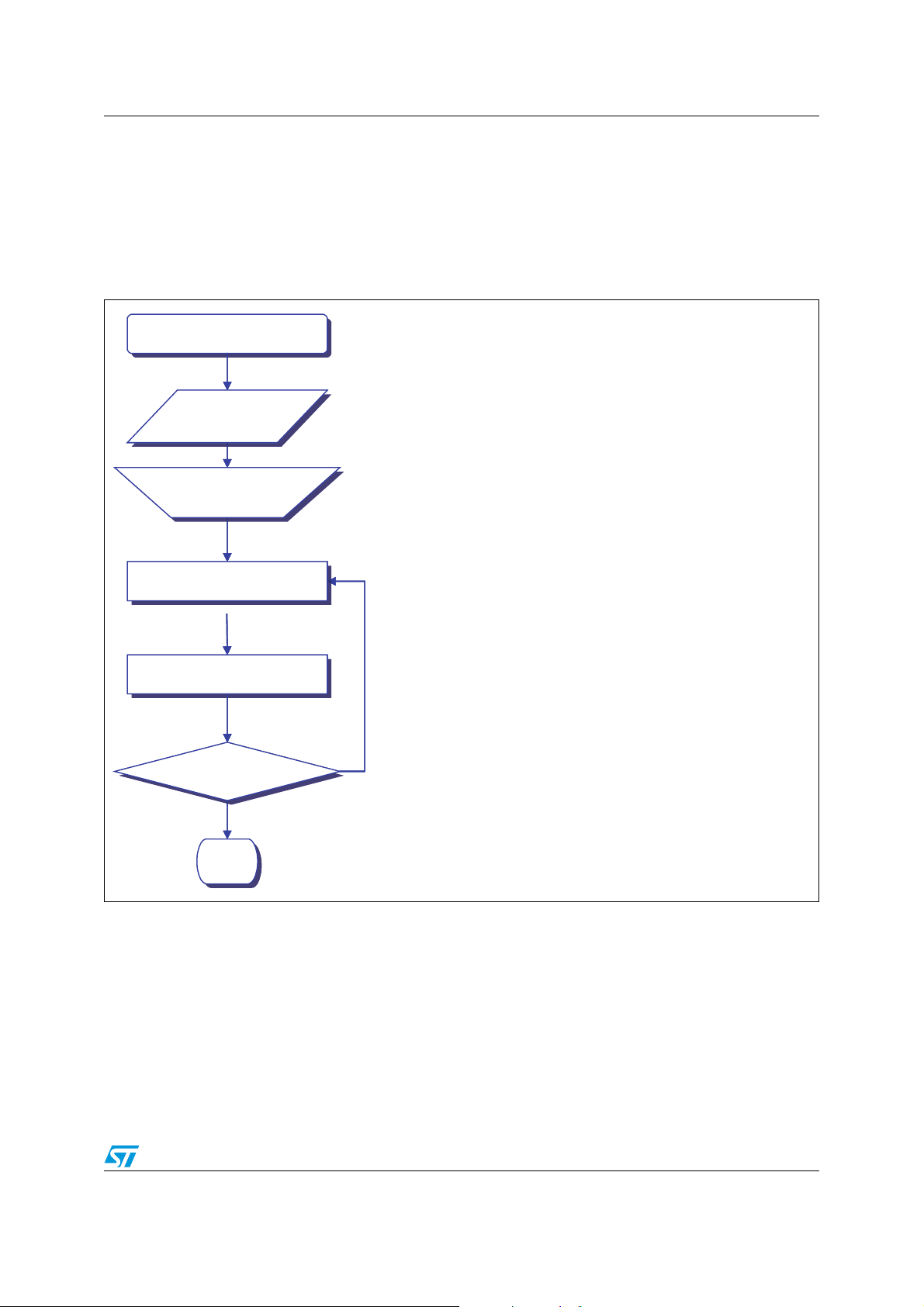
The calibration procedure can be summarized in the following steps, which are examined in
Section 1.1.
Figure 1. Calibration flow chart
Start
Start
Start
Start
Working point
Working point
Working point
Working point
R1 or SV
R1 or SV
R1 or SV
R1 or SV
1. Working point setting
2. Algorithm choice
Offline
Offline
Offline
Offline
Online
Online
Online
Online
Decrease LED frequency
K?
K?
K?
K?
End
End
End
End
1.1 Calibration procedure
1.1.1 Working point setting
According to the information contained in AN2299, the STPMC1 device can also be
calibrated in a single point for each phase.
3. Offline parameters calculations
4. Online procedure (for each phase)
5. Coherency check (for each phase)
AM09391v1
Therefore, voltage and current nominal values of the selected phase must be defined before
running the calibration procedure, for example:
Doc ID 018812 Rev 1 3/11
Page 4

Calibration flow chart AN3398
Table 1. Working point setting
Parameter Value Description
Vn 230 V Phase to neutral RMS voltage
In 5 A Phase RMS current
The other parameters, which follow, and the constants of the STPMC1 metering device (and
relative tolerances) are also known:
Table 2. STPMC1 internal parameters
Parameter Value Description
Kint_comp 1.004 Gain of decimation filter
0.875 Voltage calibrator ideal value if PM = 0
K
V
0.9375 Voltage calibrator ideal value if PM = 1
0.875 Current calibrator ideal value if PM = 0
K
I
0.9375 Current calibrator ideal value if PM = 1
len_i 2^16 Current register length
len_u 2^12 Voltage register length
π
3.14159
(1)
4 * 10^6 If oscillator frequency is 4.000 or 8.000 MHz
FM
2^22 If oscillator frequency is 4.194 or 8.388 MHz
4915200 If oscillator frequency is 4.915 or 9.830 MHz
D
UD
2^17 Internal parameter
Vref 1.23 Internal voltage reference
4 Amplification of voltage ADC for STPMS1
Au
2 Amplification of voltage ADC for STPMS2
8
Amplification of current ADC for STPMS1
32
Ai
2
Amplification of current ADC for STPMS2
16
0.815 Gain of integrator @ line frequency = 50 Hz
Kint
0.679 Gain of integrator @ line frequency = 60 Hz
0.6135 Gain of differentiator @ line frequency = 50 Hz
Kdif
0.7359 Gain of differentiator @ line frequency = 60 Hz
1. PM is CFG 21, which sets the meter precision (Class 1 or Class 0.1).
4/11 Doc ID 018812 Rev 1
Page 5

AN3398 Calibration flow chart
Only analog parameters are objects of calibration because they introduce a certain error.
Voltage ADC amplification Av is constant, while Ai is chosen according to the used sensors.
The calibration procedure has, as a final result, correction parameters called K
and K
, KIS, KIT and KIN (if used) which, applied to STPMC1 voltage and current
IR
, KVS, KVT
VR
measurements, compensate small tolerances of analog components that affect energy
calculations.
As K
, KVS, KVT and KIR, KIS, KIT and KIN calibration parameters are the decimal
VR
representation of the corresponding configuration bytes CVR, CVS, CVT and CIR, CIS, CIT,
CIN, the values of those bits are obtained at the end of calibration.
In the following procedure CVR, CVS, and CVT are indicated as Cv; CIR, CIS, CIT, and CIN
are indicated as Ci; K
, KVS, and KVT are indicated as Kv, and KIR, KIS, KIT, and KIN are
VR
indicated as Ki.
Through hardwired formulas, Kv and Ki tune measured values varying from 0.75 to 1 in 256
steps, according to the value of Cv and Ci (from 0 to 255).
If PM=1, two bits are appended to each Cv and Ci (see the STPMC1 datasheet for details),
and the corresponding tunings vary from 0.875 to 1 in 1024 steps.
To initially obtain the greatest correction dynamic, calibrators are set in the middle of the
range, therefore obtaining a calibration range of ± 12.5% (± 6.25% when PM is set) per
voltage or current channel:
Table 3. Calibrator value according to PM
PM Calibrator value
0
1
Kv = Ki = 0.875
Ci = Cv = 128
Kv = Ki = 0.9375
Ci = Cv = 512
In this way it is possible to tune Kv and Ki having a precise measurement: for example, with
PM=0, Cv=0 generates a correction factor of -12.5% (Kv=0.75) and Cv=255 determines a
correction factor of +12.5% (Kv=1), and so on.
According to the information above, the following formulas, which relate Kv,i and Cv,i to each
other are obtained:
Equation 1
Kv,i = (Cv,i/128) * 0.125 + 0.75
Equation 2
Cv,i = 1024 * Kv,i - 768
or when PM = 1
Equation 3
Kv,i = (Cv,i/512) * 0.0625 + 0.875
Equation 4
Doc ID 018812 Rev 1 5/11
Page 6

Calibration flow chart AN3398
Cv,i = 8192 * Kv,i - 7168
Indicating, with AvI and AvV, the average values read from the device and with X
ideal values of RMS current and voltage readings, the following can be reported:
PM = 0:
Equation 5
X
= (Kv * AvV) / 0.875
V
Equation 6
X
= (Ki * AvI) / 0.875
I
PM = 1:
Equation 7
X
= (Kv * AvV) / 0.9375
V
Equation 8
X
= (Ki * AvI) / 0.9375
I
1.1.2 Algorithm choice
It is possible to use two different algorithms to calculate the parameters to be used during
calibration:
1. R
2. Current sensor sensitivity and R2 constant in order to carry out R1.
and R2 constant in order to carry out the sensor sensitivity K
1
and XV the
I
S
The methods are the same and the choice is left to the designer.
According to the chosen algorithm, the next calibration step produces the value of sensor K
or resistor R
to be mounted on the measurement board to achieve calibration.
1
Algorithm formulas are reported below for both current transformer/Shunt and Rogowski coil
current sensors.
1.1.3 Offline parameter calculations
First of all, it is necessary to determine the target power sensitivity (from the LED pin) to be
achieved with the calibration process, for example:
C = 128000 pulses/kWh
The calibration procedure outputs Cv and Ci values that allow the above power sensitivity of
the meter.
This sensitivity is used to calculate target frequency at the LED pin for nominal voltage and
current values:
Equation 9
X
= f * 64
F
with:
Equation 10
S
6/11 Doc ID 018812 Rev 1
Page 7

AN3398 Calibration flow chart
f = (C/64 * In * Vn) / 3600000
Current transformer or Shunt - Constant R
1
In this algorithm voltage divider sensitivity is fixed, therefore, resistor values R1 and R2 are
the known values of the voltage divider resistor.
From the values above and for both the given amplification factor Ai and the initial calibration
data, the following target values can be calculated:
Voltage divider output:
Equation 11
V
= Vn * R2 / (R1 + R2)
DIV
Target RMS reading for given Vn:
Equation 12
X
= (V
V
DIV
/ V
) * 2 * Kdif * Av * Kv * Kint_comp* Kint * len_u
REF
Target RMS reading for given In:
Equation 13
X
= f * len_u * len_i * DUD / (FM * XV)
I
From which current sensor sensitivity K
is obtained:
S
Equation 14
K
= XI * V
S
* 1000 / (In * Ai * Ki * Kint_comp * Kint * Kdif * len_i) [mV/A]
REF
Current transformer or Shunt - Constant KS
In this case the type of current sensor and its nominal value of sensitivity must be known
and is equal to K
From the values above and for both the given amplification factor Ai and the initial calibration
data, the following target values can be calculated:
Target RMS reading for given In:
Equation 15
X
= In * KS * Ai * Ki * Kint * Kint_comp * Kdif * len_i / (V
I
Target RMS reading for given Vn:
Equation 16
X
= f * len_u * len_i * DUD / (FM * XI)
V
Voltage divider output:
Equation 17
V
= XV * V
DIV
From which R1 resistor value is obtained:
.
S
/ (2 * Kdif * Av * Kv * Kint_comp * Kint * len_u)
REF
REF
* 1000)
Equation 18
Doc ID 018812 Rev 1 7/11
Page 8

Calibration flow chart AN3398
R1 = R2 * (Vn - V
Rogowski coil - Constant R
DIV
) / V
DIV
[Ohm]
1
As before, the voltage divider sensitivity is fixed, therefore, resistor values R1 and R2 are the
known values of the voltage divider resistor.
From the values above and for both the given amplification factor Ai and the initial calibration
data, the following target values can be calculated:
Voltage divider output:
Equation 19
V
= Vn * R2 / (R1 + R2)
DIV
Target RMS reading for given Vn:
Equation 20
X
= (V
V
DIV
/ V
) * Av * Kv * Kint_comp * len_u
REF
Target RMS reading for given In:
Equation 21
X
= f * len_u * len_i * DUD / (FM * XV)
I
From which current sensor sensitivity K
is obtained:
S
Equation 22
K
= XI * V
S
Rogowski coil - Constant K
* 1000 / (In * Ai * Ki * Kint_comp * Kint * len_i) [mV/A]
REF
S
The sensor’s nominal value of sensitivity must again be known, for example, it is KS.
From the values above and for both the given amplification factor Ai and the initial calibration
data, the following target values can be calculated:
Target RMS reading for given In:
Equation 23
X
= In * KS * Ai * Ki * Kint * Kint_comp * len_i / (V
I
REF
* 1000)
Target RMS reading for given Vn:
Equation 24
X
= f * len_u * len_i * DUD / (FM * XI)
V
Voltage divider output:
Equation 25
V
= XV * V
DIV
From which R
/ (Av * Kv * Kint_comp * len_u)
REF
resistor value is obtained:
1
Equation 26
8/11 Doc ID 018812 Rev 1
Page 9

AN3398 Calibration flow chart
R1 = R2 * (Vn - V
DIV
) / V
1.1.4 Online procedure
According to the used current sensor and the chosen algorithm, a component (resistor or
current sensor) of the value calculated through the formulas above must be mounted on the
board.
To start the online calibration procedure, the following must be verified:
● EM is connected to the calibration system and is properly configured according to the
chosen application
● EM calibrator parameters are preset to initial data
● Target values of line signals are stable.
A 3-phase voltage signal must be provided to all phases and current signal only to the phase
under calibration.
When the system is connected and powered on, a certain number of readings of the RMS
values must be performed.
Due to the fact that 0.4% of ripple is present in the measured RMS values, more than ten
readings of these values should be gathered each cycle (20 ms at 50 Hz) and the average
values of RMS current and voltage readings AvI and AvV should be computed.
Consequently, having the average values AvI and AvV, a pair of final 8-bit (or 10-bit if PM =
1) calibration data can be calculated as shown below:
DIV
[Ohm]
Equation 27
Ci,v = 896 * X
/ AvI, V - 768; (PM = 0)
I,V
Equation 28
Ci,v = 8192 * X
where X
and XI are those calculated in one of the four previous cases.
V
/ AvI, V - 7168; (PM = 1)
I,V
1.1.5 Coherency check
We can assume that the EM works correctly and that built-in voltage and current sensors
allow the target power sensitivity constant to be achieved, because the correction
parameters Ki and Kv can tune measured values within the calibration range of ±12.5% or
±6.25% if PM =1 per voltage or current channel.
If, after the calibration, calculated values for Cv or Ci are out of their 8 or 10-bit range, it may
mean that the application cannot reach the target value of power sensitivity. In this case,
steps 3 and 4 must be repeated choosing a smaller power sensitivity value. If the values of
Cv or Ci are out of range even for small values of PM, it may mean that the energy meter
board is not good enough to perform such measurements, possibly because the tolerance
of the components is too big, or no care has been taken in the layout phase, so the
application must be re-designed.
Otherwise, if the final calibrator data is written into STPMC1, the average RMS readings are
very close to target values X
the target value f.
and XV and the frequency of the LED output are very close to
I
Doc ID 018812 Rev 1 9/11
Page 10

Revision history AN3398
2 Revision history
Table 4. Document revision history
Date Revision Changes
16-Nov-2011 1 First release
10/11 Doc ID 018812 Rev 1
Page 11

AN3398
Please Read Carefully:
Information in this document is provided solely in connection with ST products. STMicroelectronics NV and its subsidiaries (“ST”) reserve the
right to make changes, corrections, modifications or improvements, to this document, and the products and services described herein at any
time, without notice.
All ST products are sold pursuant to ST’s terms and conditions of sale.
Purchasers are solely responsible for the choice, selection and use of the ST products and services described herein, and ST assumes no
liability whatsoever relating to the choice, selection or use of the ST products and services described herein.
No license, express or implied, by estoppel or otherwise, to any intellectual property rights is granted under this document. If any part of this
document refers to any third party products or services it shall not be deemed a license grant by ST for the use of such third party products
or services, or any intellectual property contained therein or considered as a warranty covering the use in any manner whatsoever of such
third party products or services or any intellectual property contained therein.
UNLESS OTHERWISE SET FORTH IN ST’S TERMS AND CONDITIONS OF SALE ST DISCLAIMS ANY EXPRESS OR IMPLIED
WARRANTY WITH RESPECT TO THE USE AND/OR SALE OF ST PRODUCTS INCLUDING WITHOUT LIMITATION IMPLIED
WARRANTIES OF MERCHANTABILITY, FITNESS FOR A PARTICULAR PURPOSE (AND THEIR EQUIVALENTS UNDER THE LAWS
OF ANY JURISDICTION), OR INFRINGEMENT OF ANY PATENT, COPYRIGHT OR OTHER INTELLECTUAL PROPERTY RIGHT.
UNLESS EXPRESSLY APPROVED IN WRITING BY TWO AUTHORIZED ST REPRESENTATIVES, ST PRODUCTS ARE NOT
RECOMMENDED, AUTHORIZED OR WARRANTED FOR USE IN MILITARY, AIR CRAFT, SPACE, LIFE SAVING, OR LIFE SUSTAINING
APPLICATIONS, NOR IN PRODUCTS OR SYSTEMS WHERE FAILURE OR MALFUNCTION MAY RESULT IN PERSONAL INJURY,
DEATH, OR SEVERE PROPERTY OR ENVIRONMENTAL DAMAGE. ST PRODUCTS WHICH ARE NOT SPECIFIED AS "AUTOMOTIVE
GRADE" MAY ONLY BE USED IN AUTOMOTIVE APPLICATIONS AT USER’S OWN RISK.
Resale of ST products with provisions different from the statements and/or technical features set forth in this document shall immediately void
any warranty granted by ST for the ST product or service described herein and shall not create or extend in any manner whatsoever, any
liability of ST.
ST and the ST logo are trademarks or registered trademarks of ST in various countries.
Information in this document supersedes and replaces all information previously supplied.
The ST logo is a registered trademark of STMicroelectronics. All other names are the property of their respective owners.
© 2011 STMicroelectronics - All rights reserved
STMicroelectronics group of companies
Australia - Belgium - Brazil - Canada - China - Czech Republic - Finland - France - Germany - Hong Kong - India - Israel - Italy - Japan -
Malaysia - Malta - Morocco - Philippines - Singapore - Spain - Sweden - Switzerland - United Kingdom - United States of America
www.st.com
Doc ID 018812 Rev 1 11/11
 Loading...