

AN3392
Application note
Designing with the SPV1020, an interleaved boost converter with
MPPT algorithm
By Domenico Ragonese, Massimiliano Ragusa
Introduction
The SPV1020 is a monolithic DC-DC boost converter designed to maximize the power
generated by photovoltaic panels independent of temperature and the amount of solar
radiation. The optimization of the power conversion is obtained with embedded logic which
performs the MPPT (maximum power point tracking) algorithm on the PV cells connected to
the converter.
One or more converters can be housed in the junction box of PV panels, replacing the
bypass diodes. Because of the fact that the maximum power point is locally computed, the
efficiency at system level is higher compared to the use of conventional topologies, where
the MPPT is computed in the main centralized inverter.
For a cost effective application and miniaturized solution, the SPV1020 embeds the Power
MOSFETs for active switching and synchronous rectification, minimizing the number of
external devices. Furthermore, the 4-phase interleaved topology of the DC-DC converter
avoids the use of electrolytic capacitors, which can severely limit the system lifetime.
The SPV1020 operates at fixed frequency in PWM mode, where the duty cycle is controlled
by embedded logic running a Perturb&Observe MPPT algorithm. The switching frequency,
internally generated and set by default at 100 kHz, is externally adjustable, while the duty
cycle can range from 5% to 90% in steps of 0.2%.
Safety of the application is guaranteed by stopping the drivers in the case of output
overvoltage or overtemperature.
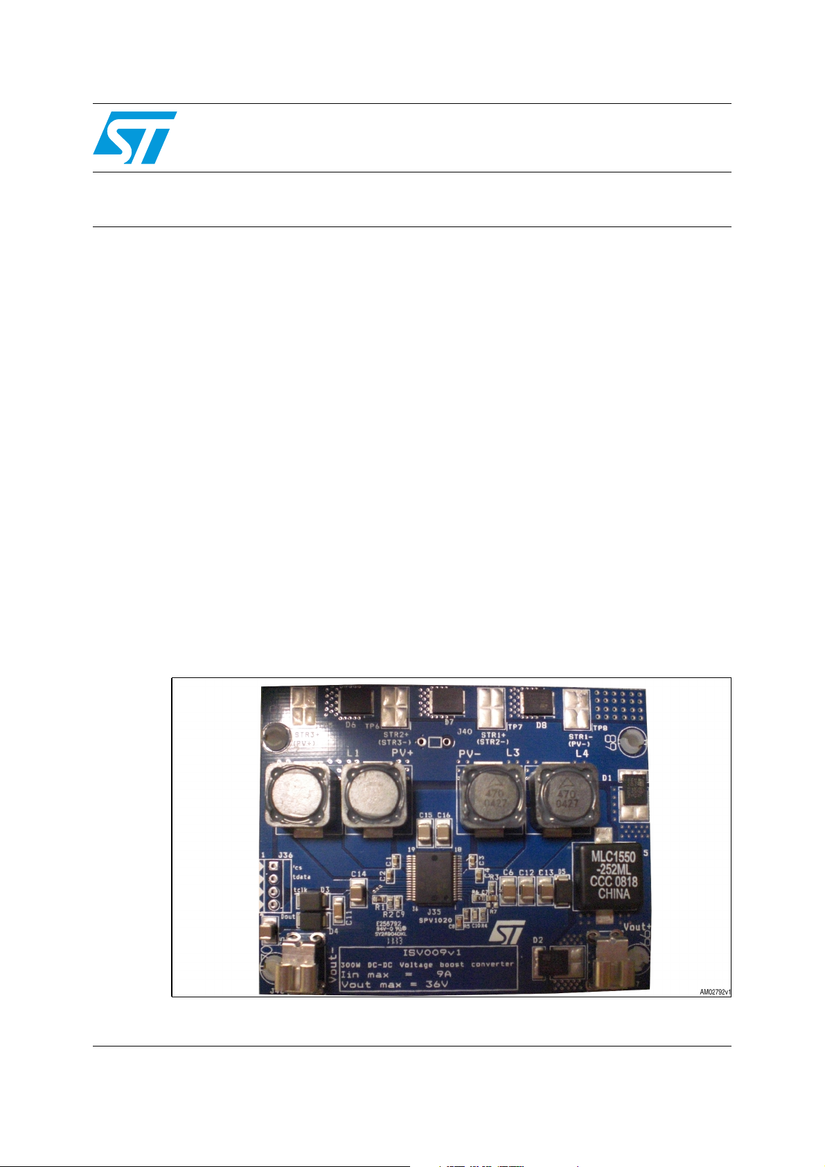
Figure 1. STEVAL-ISV009V1 demonstration board
May 2012 Doc ID 018749 Rev 1 1/57
www.st.com

Contents AN3392
Contents
1 Application overview . . . . . . . . . . . . . . . . . . . . . . . . . . . . . . . . . . . . . . . . 5
2 Application information . . . . . . . . . . . . . . . . . . . . . . . . . . . . . . . . . . . . . . 8
3 SPV1020 description . . . . . . . . . . . . . . . . . . . . . . . . . . . . . . . . . . . . . . . . 10
4 Output voltage ripple . . . . . . . . . . . . . . . . . . . . . . . . . . . . . . . . . . . . . . . 12
5 Application efficiency . . . . . . . . . . . . . . . . . . . . . . . . . . . . . . . . . . . . . . . 13
6 SPV1020 functions . . . . . . . . . . . . . . . . . . . . . . . . . . . . . . . . . . . . . . . . . 14
6.1 Operating modes. . . . . . . . . . . . . . . . . . . . . . . . . . . . . . . . . . . . . . . . . . . . 14
6.2 OFF-state . . . . . . . . . . . . . . . . . . . . . . . . . . . . . . . . . . . . . . . . . . . . . . . . . 14
6.3 Burst mode . . . . . . . . . . . . . . . . . . . . . . . . . . . . . . . . . . . . . . . . . . . . . . . . 15
6.4 Normal/MPPT mode . . . . . . . . . . . . . . . . . . . . . . . . . . . . . . . . . . . . . . . . . 15
7 Voltage regulation . . . . . . . . . . . . . . . . . . . . . . . . . . . . . . . . . . . . . . . . . . 21
7.1 Overvoltage protection . . . . . . . . . . . . . . . . . . . . . . . . . . . . . . . . . . . . . . . 21
7.2 Overcurrent protection . . . . . . . . . . . . . . . . . . . . . . . . . . . . . . . . . . . . . . . 21
7.3 Current balance . . . . . . . . . . . . . . . . . . . . . . . . . . . . . . . . . . . . . . . . . . . . 21
7.4 SPI serial peripheral interface . . . . . . . . . . . . . . . . . . . . . . . . . . . . . . . . . 22
8 Pin description . . . . . . . . . . . . . . . . . . . . . . . . . . . . . . . . . . . . . . . . . . . . 25
8.1 Pin connection . . . . . . . . . . . . . . . . . . . . . . . . . . . . . . . . . . . . . . . . . . . . . 26
9 Absolute maximum ratings . . . . . . . . . . . . . . . . . . . . . . . . . . . . . . . . . . 27
10 External component selection . . . . . . . . . . . . . . . . . . . . . . . . . . . . . . . . 28
10.1 Power and thermal considerations . . . . . . . . . . . . . . . . . . . . . . . . . . . . . . 29
10.2 Inductor selection . . . . . . . . . . . . . . . . . . . . . . . . . . . . . . . . . . . . . . . . . . . 29
10.3 Bootstrap capacitors . . . . . . . . . . . . . . . . . . . . . . . . . . . . . . . . . . . . . . . . . 30
10.4 Internal voltage rail capacitors . . . . . . . . . . . . . . . . . . . . . . . . . . . . . . . . . 31
10.5 Input voltage capacitors . . . . . . . . . . . . . . . . . . . . . . . . . . . . . . . . . . . . . . 31
10.6 Input voltage partitioning . . . . . . . . . . . . . . . . . . . . . . . . . . . . . . . . . . . . . 31
2/57 Doc ID 018749 Rev 1

AN3392 Contents
10.7 Input voltage sensing capacitor . . . . . . . . . . . . . . . . . . . . . . . . . . . . . . . . 32
10.8 Output voltage capacitors . . . . . . . . . . . . . . . . . . . . . . . . . . . . . . . . . . . . . 32
10.9 Output voltage partitioning . . . . . . . . . . . . . . . . . . . . . . . . . . . . . . . . . . . . 33
10.10 Output voltage sensing capacitor . . . . . . . . . . . . . . . . . . . . . . . . . . . . . . . 34
10.11 Internal oscillator frequency . . . . . . . . . . . . . . . . . . . . . . . . . . . . . . . . . . . 34
10.12 Diode selection . . . . . . . . . . . . . . . . . . . . . . . . . . . . . . . . . . . . . . . . . . . . . 35
10.13 Protection devices . . . . . . . . . . . . . . . . . . . . . . . . . . . . . . . . . . . . . . . . . . 35
10.14 Pole-zero compensation . . . . . . . . . . . . . . . . . . . . . . . . . . . . . . . . . . . . . . 35
11 Layout guidelines . . . . . . . . . . . . . . . . . . . . . . . . . . . . . . . . . . . . . . . . . . 36
12 Bill of material . . . . . . . . . . . . . . . . . . . . . . . . . . . . . . . . . . . . . . . . . . . . . 38
Appendix A STEVAL-ISV009V1 application diagram. . . . . . . . . . . . . . . . . . . . . . 40
Appendix B SPV1020 parallel and series connection . . . . . . . . . . . . . . . . . . . . . 41
B.1 SPV1020 parallel connection . . . . . . . . . . . . . . . . . . . . . . . . . . . . . . . . . . 42
B.2 SPV1020 series connection . . . . . . . . . . . . . . . . . . . . . . . . . . . . . . . . . . . 43
Appendix C . . . . . . . . . . . . . . . . . . . . . . . . . . . . . . . . . . . . . . . . . . . . . . . . . . . . . . . 46
C.1 Power efficiency, MPPT efficiency and thermal analysis. . . . . . . . . . . . . . 46
13 Package mechanical data . . . . . . . . . . . . . . . . . . . . . . . . . . . . . . . . . . . . 53
14 Revision history . . . . . . . . . . . . . . . . . . . . . . . . . . . . . . . . . . . . . . . . . . . 55
Doc ID 018749 Rev 1 3/57

List of figures AN3392
List of figures
Figure 1. STEVAL-ISV009V1 demonstration board . . . . . . . . . . . . . . . . . . . . . . . . . . . . . . . . . . . . . . 1
Figure 2. SPV1020 output series connection. . . . . . . . . . . . . . . . . . . . . . . . . . . . . . . . . . . . . . . . . . . . 6
Figure 3. Photovoltaic system with multi-string inverter . . . . . . . . . . . . . . . . . . . . . . . . . . . . . . . . . . . . 7
Figure 4. Photovoltaic panel for a distributed architecture. . . . . . . . . . . . . . . . . . . . . . . . . . . . . . . . . . 8
Figure 5. Step-up converter single-ended architecture . . . . . . . . . . . . . . . . . . . . . . . . . . . . . . . . . . . . 9
Figure 6. Step-up converter in continuous mode . . . . . . . . . . . . . . . . . . . . . . . . . . . . . . . . . . . . . . . . . 9
Figure 7. Step-up converter in discontinuous mode . . . . . . . . . . . . . . . . . . . . . . . . . . . . . . . . . . . . . 10
Figure 8. Boost converter interleaved 4-phase architecture . . . . . . . . . . . . . . . . . . . . . . . . . . . . . . . 11
Figure 9. Synchronous rectification and zero crossing block . . . . . . . . . . . . . . . . . . . . . . . . . . . . . . . 12
Figure 10. Boost IL-4 and SPV1020 . . . . . . . . . . . . . . . . . . . . . . . . . . . . . . . . . . . . . . . . . . . . . . . . . . 12
Figure 11. Step-up current waveforms or interleaved 4-phase architecture . . . . . . . . . . . . . . . . . . . . 13
Figure 12. SPV1020 general FSM (finite state machine). . . . . . . . . . . . . . . . . . . . . . . . . . . . . . . . . . . 15
Figure 13. Burst mode FSM . . . . . . . . . . . . . . . . . . . . . . . . . . . . . . . . . . . . . . . . . . . . . . . . . . . . . . . . . 16
Figure 14. SPV1020 MPPT block . . . . . . . . . . . . . . . . . . . . . . . . . . . . . . . . . . . . . . . . . . . . . . . . . . . . 17
Figure 15. SPV1020 equivalent circuit . . . . . . . . . . . . . . . . . . . . . . . . . . . . . . . . . . . . . . . . . . . . . . . . . 17
Figure 16. PV panels, power vs. voltage and current vs. voltage curves . . . . . . . . . . . . . . . . . . . . . . 18
Figure 17. MPPT data flow diagram . . . . . . . . . . . . . . . . . . . . . . . . . . . . . . . . . . . . . . . . . . . . . . . . . . 18
Figure 18. MPPT concept flow diagram . . . . . . . . . . . . . . . . . . . . . . . . . . . . . . . . . . . . . . . . . . . . . . . . 19
Figure 19. Normal/MPPT mode, DCM vs. CM FSM . . . . . . . . . . . . . . . . . . . . . . . . . . . . . . . . . . . . . . 20
Figure 20. Input voltage partitioning, sample circuit. . . . . . . . . . . . . . . . . . . . . . . . . . . . . . . . . . . . . . . 21
Figure 21. SPI interface: master/slaves connection example . . . . . . . . . . . . . . . . . . . . . . . . . . . . . . . 23
Figure 22. Frame structure: register read operation . . . . . . . . . . . . . . . . . . . . . . . . . . . . . . . . . . . . . . 24
Figure 23. Pin connection top view PowerSSO-36 . . . . . . . . . . . . . . . . . . . . . . . . . . . . . . . . . . . . . . . 27
Figure 24. STEVAL-ISV009V1 schematic (PowerSSO-36 package). . . . . . . . . . . . . . . . . . . . . . . . . . 29
Figure 25. PCB layout example (top view). . . . . . . . . . . . . . . . . . . . . . . . . . . . . . . . . . . . . . . . . . . . . . 37
Figure 26. PCB layout example (bottom view). . . . . . . . . . . . . . . . . . . . . . . . . . . . . . . . . . . . . . . . . . . 38
Figure 27. STEVAL-ISV009V1 application schematic . . . . . . . . . . . . . . . . . . . . . . . . . . . . . . . . . . . . . 41
Figure 28. SPV1020, output parallel connection . . . . . . . . . . . . . . . . . . . . . . . . . . . . . . . . . . . . . . . . . 43
Figure 29. SPV1020, output series connection . . . . . . . . . . . . . . . . . . . . . . . . . . . . . . . . . . . . . . . . . . 44
Figure 30. Measurement environment . . . . . . . . . . . . . . . . . . . . . . . . . . . . . . . . . . . . . . . . . . . . . . . . . 47
Figure 31. Power efficiency vs. output voltage . . . . . . . . . . . . . . . . . . . . . . . . . . . . . . . . . . . . . . . . . . 48
Figure 32. Power efficiency vs. output voltage . . . . . . . . . . . . . . . . . . . . . . . . . . . . . . . . . . . . . . . . . . 48
Figure 33. Power efficiency vs. output voltage . . . . . . . . . . . . . . . . . . . . . . . . . . . . . . . . . . . . . . . . . . 49
Figure 34. MPPT accuracy vs. output voltage . . . . . . . . . . . . . . . . . . . . . . . . . . . . . . . . . . . . . . . . . . . 49
Figure 35. MPPT accuracy vs. output voltage . . . . . . . . . . . . . . . . . . . . . . . . . . . . . . . . . . . . . . . . . . . 50
Figure 36. MPPT accuracy vs. output voltage . . . . . . . . . . . . . . . . . . . . . . . . . . . . . . . . . . . . . . . . . . . 50
Figure 37. Vin = 12 V, Iin = 8 A, VOUT = 36 V, Tamb = 25 °C . . . . . . . . . . . . . . . . . . . . . . . . . . . . . . 51
Figure 38. Vin = 12 V, Iin = 8 A, VOUT = 14 V, Tamb = 25 °C . . . . . . . . . . . . . . . . . . . . . . . . . . . . . . 51
Figure 39. Vin = 24 V, Iin = 8 A, VOUT = 36 V, Tamb = 25 °C . . . . . . . . . . . . . . . . . . . . . . . . . . . . . . 52
Figure 40. Vin = 24 V, Iin = 8 A, VOUT = 26 V, Tamb = 25 °C . . . . . . . . . . . . . . . . . . . . . . . . . . . . . . 52
Figure 41. Vin = 30 V, Iin = 8 A, VOUT = 36 V, Tamb = 25 °C . . . . . . . . . . . . . . . . . . . . . . . . . . . . . . 53
Figure 42. Vin = 30 V, Iin = 8 A, VOUT = 32 V, Tamb = 25 °C . . . . . . . . . . . . . . . . . . . . . . . . . . . . . . 53
Figure 43. PowerSSO-36 package dimensions . . . . . . . . . . . . . . . . . . . . . . . . . . . . . . . . . . . . . . . . . . 55
4/57 Doc ID 018749 Rev 1

AN3392 List of tables
List of tables
Table 1. Data format for words longer than 8 bits. . . . . . . . . . . . . . . . . . . . . . . . . . . . . . . . . . . . . . . 24
Table 2. Commands list . . . . . . . . . . . . . . . . . . . . . . . . . . . . . . . . . . . . . . . . . . . . . . . . . . . . . . . . . . 25
Table 3. Pin description . . . . . . . . . . . . . . . . . . . . . . . . . . . . . . . . . . . . . . . . . . . . . . . . . . . . . . . . . . 26
Table 4. Maximum ratings . . . . . . . . . . . . . . . . . . . . . . . . . . . . . . . . . . . . . . . . . . . . . . . . . . . . . . . . 28
Table 5. Bill of material . . . . . . . . . . . . . . . . . . . . . . . . . . . . . . . . . . . . . . . . . . . . . . . . . . . . . . . . . . . 39
Table 6. PowerSSO-36 mechanical data . . . . . . . . . . . . . . . . . . . . . . . . . . . . . . . . . . . . . . . . . . . . . 54
Table 7. Document revision history . . . . . . . . . . . . . . . . . . . . . . . . . . . . . . . . . . . . . . . . . . . . . . . . . 56
Doc ID 018749 Rev 1 5/57
Application overview AN3392
1 Application overview
The following diagram shows the typical architecture of a photovoltaic system for a grid
connected application and consists of a photovoltaic field and an electronic section.
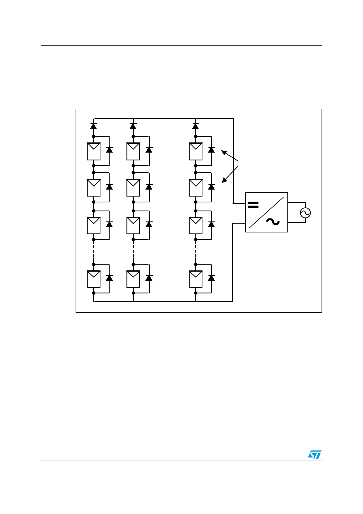
Figure 2. SPV1020 output series connection
"LOCKING
DIODES
"Y PASS
DI
ODES
'RID
)NVERTER
.
The photovoltaic field is made up of PV panels. Some PV panels are connected in series to
make a PV string. Each string is connected in parallel with the others and then connected to
the electronic section of the system, the “inverter”, which has the role of adapting the
produced power to the characteristics of the public electrical grid.
.
.
!-V
Other electronic components are the bypass diodes and the blocking diodes.
Each bypass diode protects the panel to which it is connected by providing an alternative
path for the current flow generated by other panels. These diodes guarantee both panel
protection and system functionality in case of damaged or shaded panels.
Blocking diodes (or “cut-off” diodes) protect the entire string from current following from
other strings due to a lower voltage of the string, typically caused by shadows on a part of
the string.
6/57 Doc ID 018749 Rev 1
AN3392 Application overview
Inverters are complex systems normally providing three functions (DC-DC conversion, DCAC conversion and Anti-Islanding) managed by a main controller typically implemented by a
microcontroller or DSP and executing the following actions:
● Anti-Island control, a safety control forcing the system to disconnect from the grid when
it is OFF for maintenance.
● Inverter control, for converting the DC power generated by the PV field to AC power
compatible with the power on the public grid (voltage and current amplitude, frequency
and phase).
● The MPPT (maximum power point tracking) control, allowing the extraction of the
maximum amount of power possible from the PV field in order to maximize the power
sourced to the grid.
A limitation of the architecture in Figure 2 is that the MPPT control performs properly only
when the PV field is uniformly irradiated.
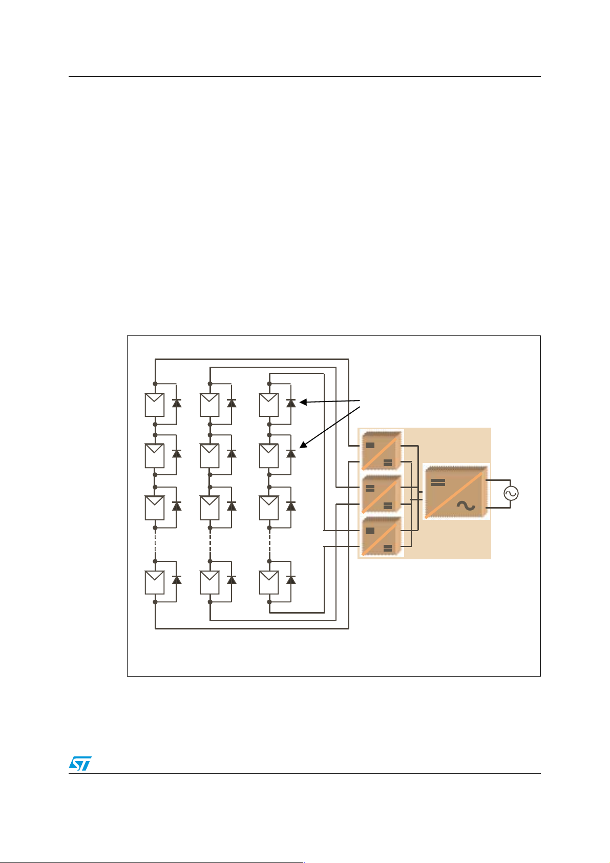
A first evolution of the above architecture is shown in Figure 3 (string-distributed), where the
inverter includes more DC-DC converter sub-blocks, each implementing its own MPPT
algorithm.
Figure 3. Photovoltaic system with multi-string inverter
"Y PASS
DI
ODES
'RID
)NVERTER
.
.
Even though this architecture provides for a different shadow on each string, it doesn’t solve
the problem of the partial shading on each panel.
.
!-V
Doc ID 018749 Rev 1 7/57
Application overview AN3392
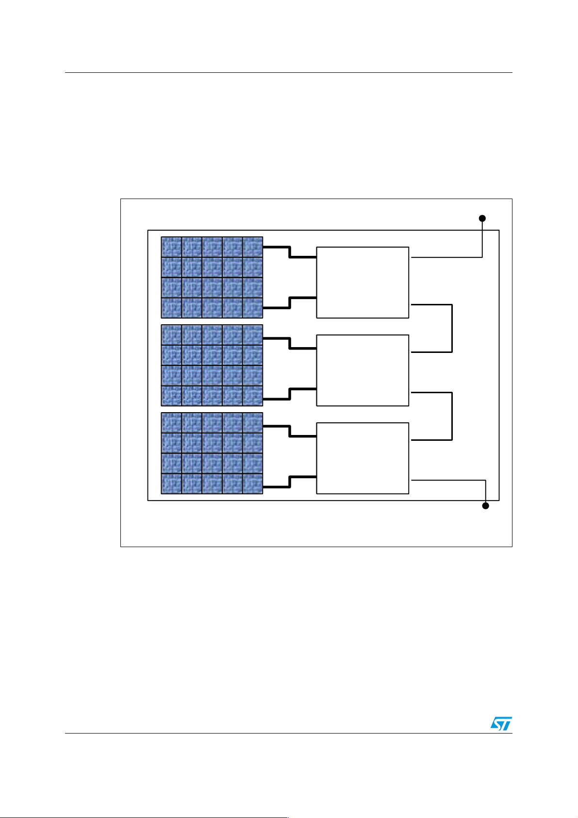
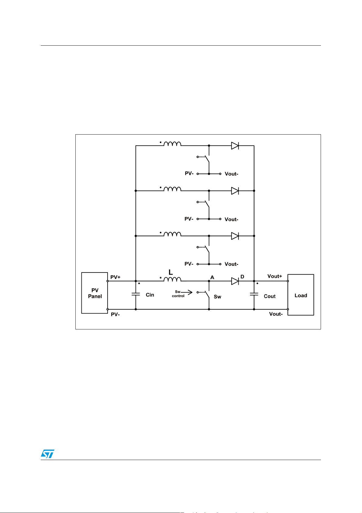
A better solution for this issue is to place the DC-DC converter and related MPPT algorithm
on each panel. This approach provides for a simpler inverter architecture that doesn’t
require a DC-DC block and related controller.
Furthermore, in order to minimize the impact of partial shading on each panel, it’s possible
to show the concept having a DC-DC converter for each cell of the panel. As a compromise
between cost and performance the following approach splits a panel into 3 different
substrings.
Figure 4. Photovoltaic panel for a distributed architecture
6O
UT
"//34
06
-004
06
06
"//34
-004
"//34
-004
DISTRIBUTED
ARCHITECTURE
6O UT
!-V
8/57 Doc ID 018749 Rev 1
AN3392 Application information
2 Application information
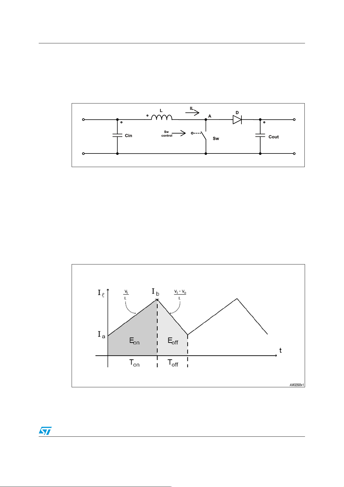
A step-up (or boost) converter is a switching DC-DC converter able to generate an output
voltage higher than the input voltage.
Figure 5. Step-up converter single-ended architecture
!-V
The switching element (Sw) is typically driven by a fixed-frequency rectangular waveform
generated by a PWM controller.
When Sw is closed (T
), the inductor stores energy and its current increases with a slope
on
depending on the voltage across the inductor and its inductance value. During this time the
output voltage is sustained by C
and the diode doesn’t allow any charge transfer from
out
output to input stages.
When Sw is open (T
) the current in the inductor flows toward the output until the voltage
off
on node “A” is higher than the output voltage. During this phase the current in the inductor
decreases while the output voltage increases.
Figure 6 shows the behavior of the current on the inductor.
Figure 6. Step-up converter in continuous mode
Comparing the energy stored in the inductor during T
the relation between V
and Vin is:
OUT
Doc ID 018749 Rev 1 9/57
and the energy released during T
on
off
,
Application information AN3392
Equation 1
V
out
-----------
V
in
-------------=
1D–
1
where “D” is the duty cycle [T
/(Ton+T
on
)] of the rectangular waveform driving the switching
off
element.
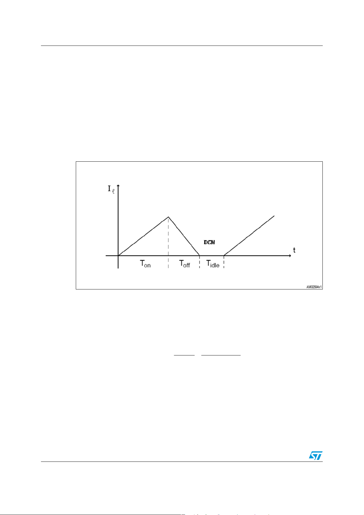
Boost converters can work in two main modes:
● Continuous mode (CM);
● Discontinuous mode (DCM);
depending on whether the current on the inductor becomes zero (DCM), or not (CM), within
the switching period.
Figure 7. Step-up converter in discontinuous mode
Even though a boost converter may work both in CM and DCM modes, efficiency is normally
higher when it works in CM, if the switching frequency is constant.
Inductance and switching frequency (F
) determine the working mode. In order to have the
sw
system working in CM, the following rule should be used:
Equation 2
Vout
L
Pin
∗>
Worst case for L in the above formula is D = 50%.
10/57 Doc ID 018749 Rev 1
22
−
))D1(*D(
Fsw*2
AN3392 SPV1020 description
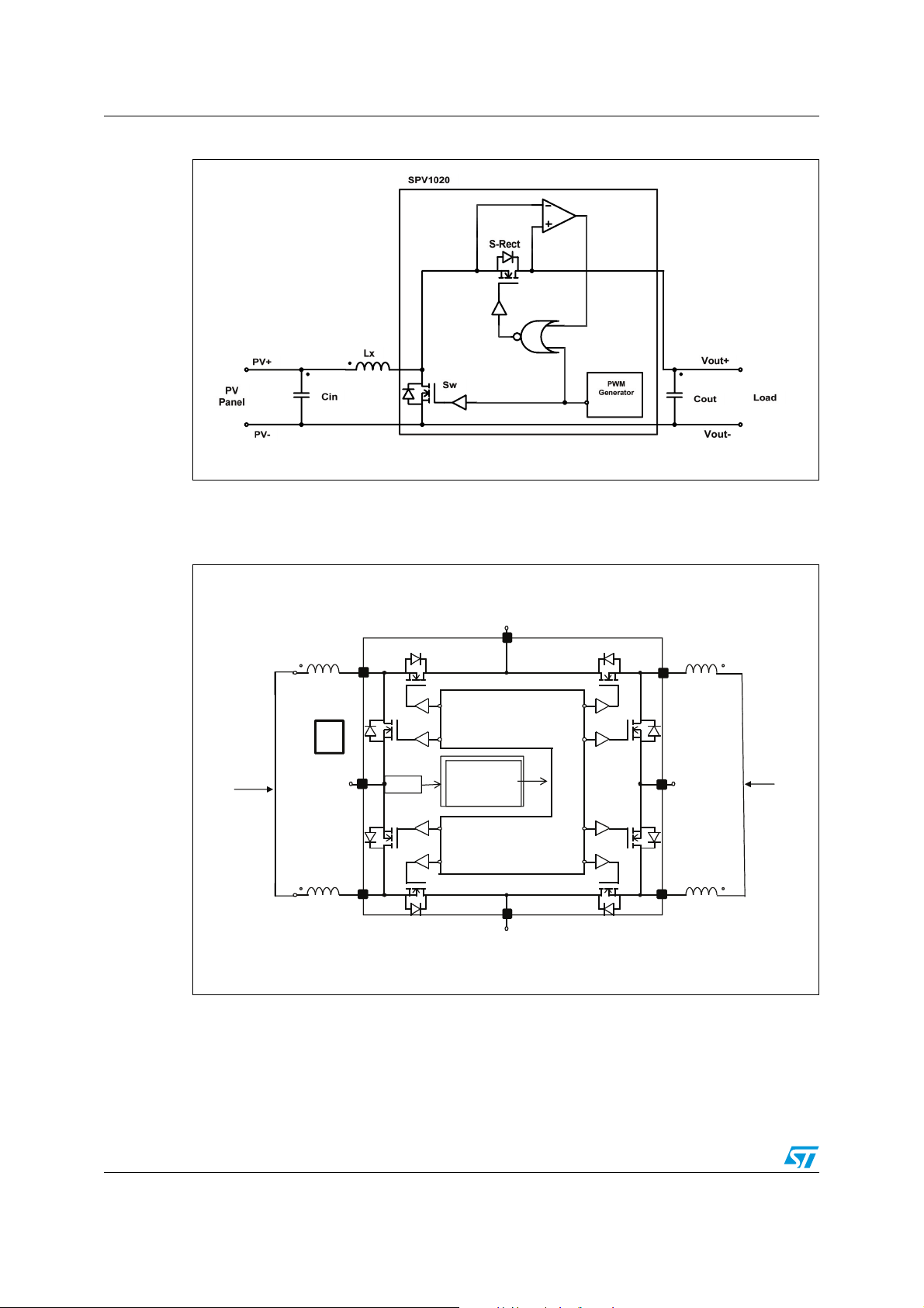
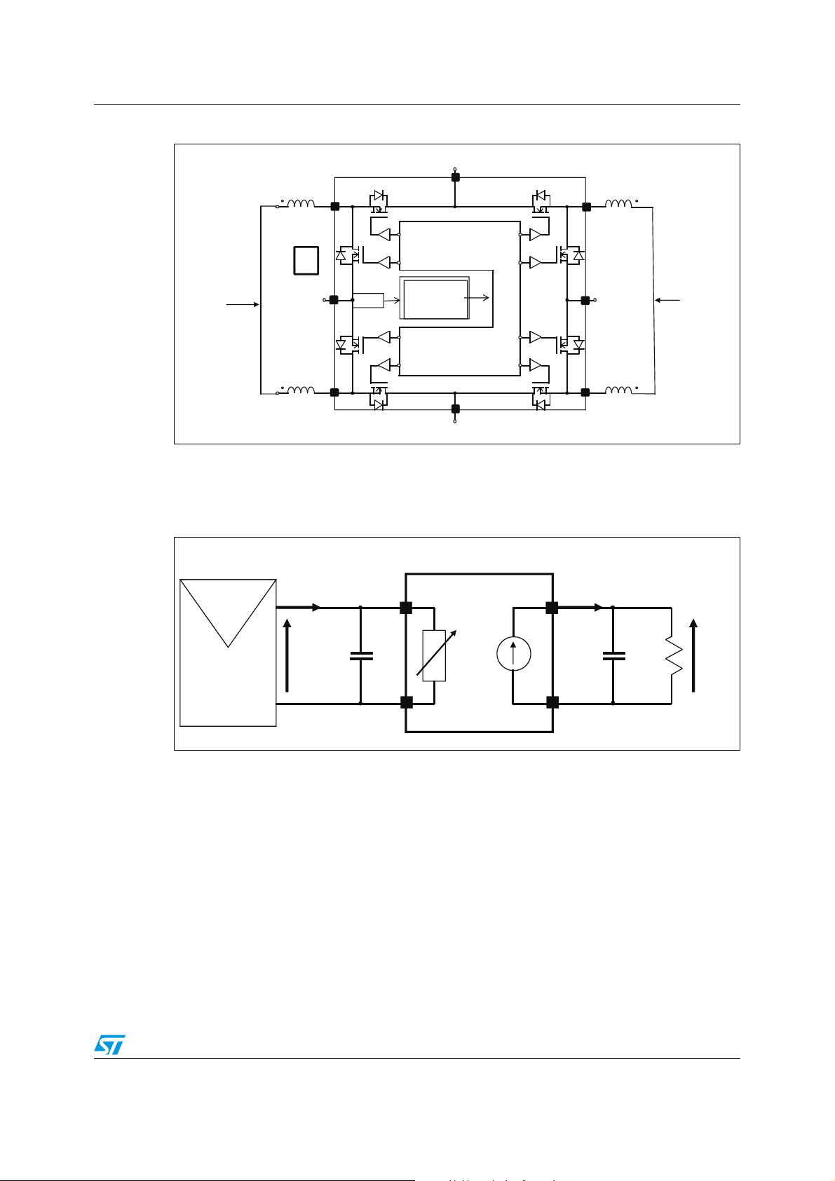
3 SPV1020 description
The SPV1020 is an IC designed to provide a boost with a 4-phase interleaved topology
when supplied by photovoltaic panels.
In a 4-phase topology, the inductor-switch-diode branch is cloned 3 times and the resulting
four branches are connected in parallel. The resulting architecture is shown in Figure 8
below:
Figure 8. Boost converter interleaved 4-phase architecture
!-V
The SPV1020 drives the four switching elements with the same waveform but shifted by
T
/4.
SW
In order to increase application efficiency each diode can be replaced by a switching
element driven complimentary with respect to the corresponding switch. Furthermore, these
four switching elements (synchronous rectifiers) must be driven in order to prevent current
flow from the output to the input.
The SPV1020 integrates four zero crossing blocks (ZCB), one for each branch. Their role is
to turn off the related synchronous rectifier to prevent reverse current flow from output to
input.
Doc ID 018749 Rev 1 11/57
SPV1020 description AN3392
Figure 9. Synchronous rectification and zero crossing block
".W
Finally, in order to minimize the entire bill of material, the SPV1020 integrates the eight
switching elements.
Figure 10. Boost IL-4 and SPV1020
VREF
PV+
PV-
MPPT
VOUT
PWM
GEN
VOUT
DC
PV-
PV+
SHIFTING
AM02597v1
Even though the interleaved topology increases the bill of material and the wiring of the final
PCB, it is preferable to the single-ended approach especially in high-power applications.
In fact, output voltage ripple and efficiency are critical parameters for boost applications.
The following is a brief description of a boost interleaved 4 (IL-4) architecture.
12/57 Doc ID 018749 Rev 1
AN3392 Output voltage ripple
4 Output voltage ripple
Assuming a resistive load, the output voltage ripple is directly related to the output current
ripple.
In a single-ended architecture, the output current is the current flowing on the inductor when
it recirculates through the rectifiers. Referring to Figure 6, the larger the inductance, the
smaller the current ripple (I
In IL-4 architecture, output current is the sum of the four currents flowing in each inductor.
Even if the current on each branch is the same as in the single-ended architecture, the
T
/4 shift between the driving signals implies that output current has a small amount of
SW
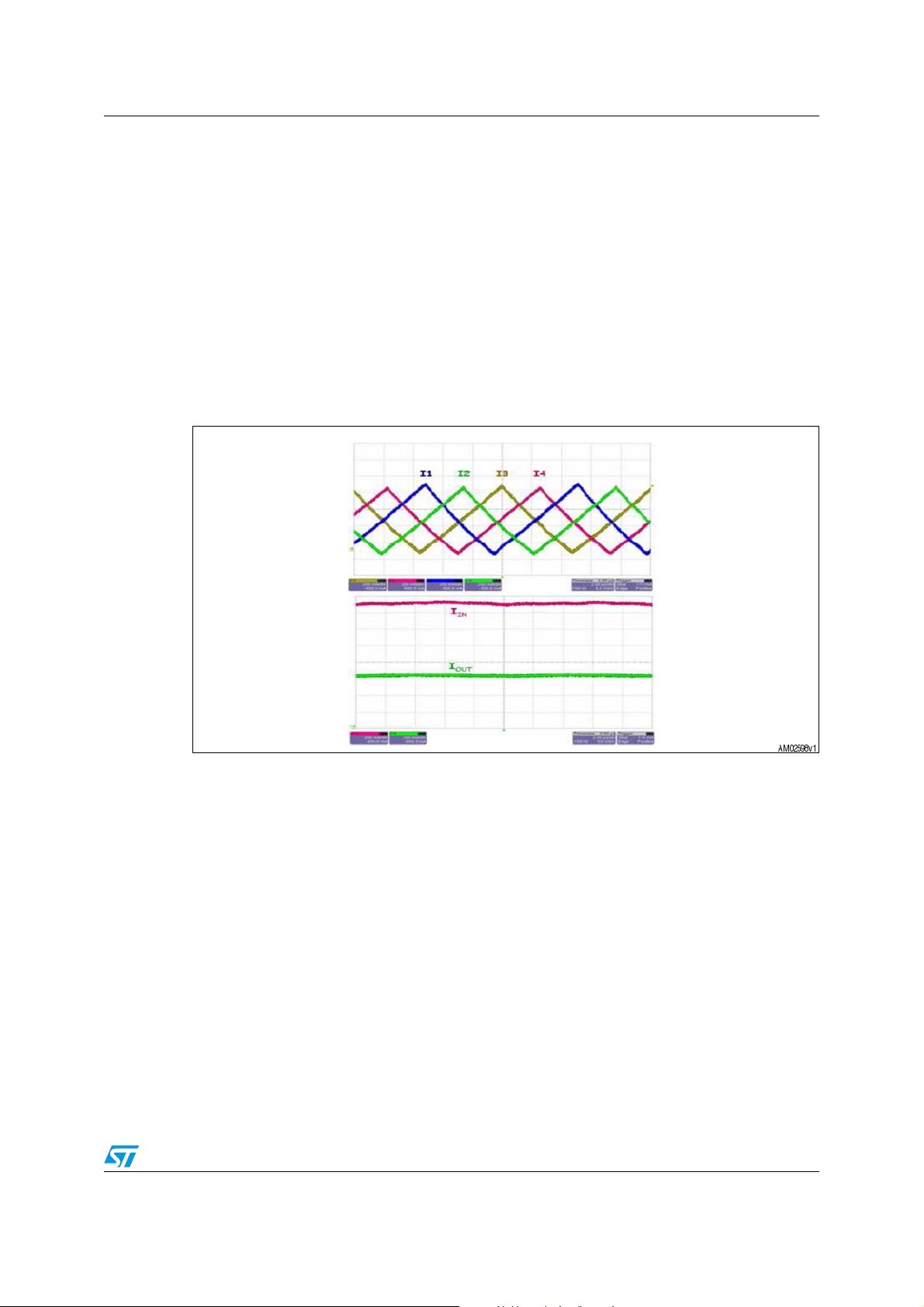
ripple. Figure 11 shows both the current in each branch and the final I
Figure 11. Step-up current waveforms or interleaved 4-phase architecture
b-Ia
).
.
OUT
With respect to single-ended architecture, input and output current ripple are significantly
reduced due to both the split of the incoming current in the four branches and the related
phase shift.
Doc ID 018749 Rev 1 13/57

Application efficiency AN3392
5 Application efficiency
In designing a boost application, a typical constraint is the maximum output current ripple.
Once frequency, input, and output voltage are defined, this ripple is directly related to the
inductance value in the application:
Equation 3
V
D
in
--------
I
rippleILmaxILmin
The inductance value can be designed for a single-ended architecture and then divided by 4
in the case of IL-4 architecture.
---------
⋅=–=
L
F
sw
Each inductor, due to its internal resistance (R
), can affect system efficiency. For high
L
current applications, an inductor with a compact geometry may compromise the efficiency
requirements.
Using the same ferromagnetic material, higher inductance can be achieved by increasing
the inductor geometry, or by increasing the number of turns but using a thinner wire.
In order to save space and cost, the latter solution is preferred but this increases the internal
resistance and the saturation current of the inductor.
14/57 Doc ID 018749 Rev 1
AN3392 SPV1020 functions
6 SPV1020 functions
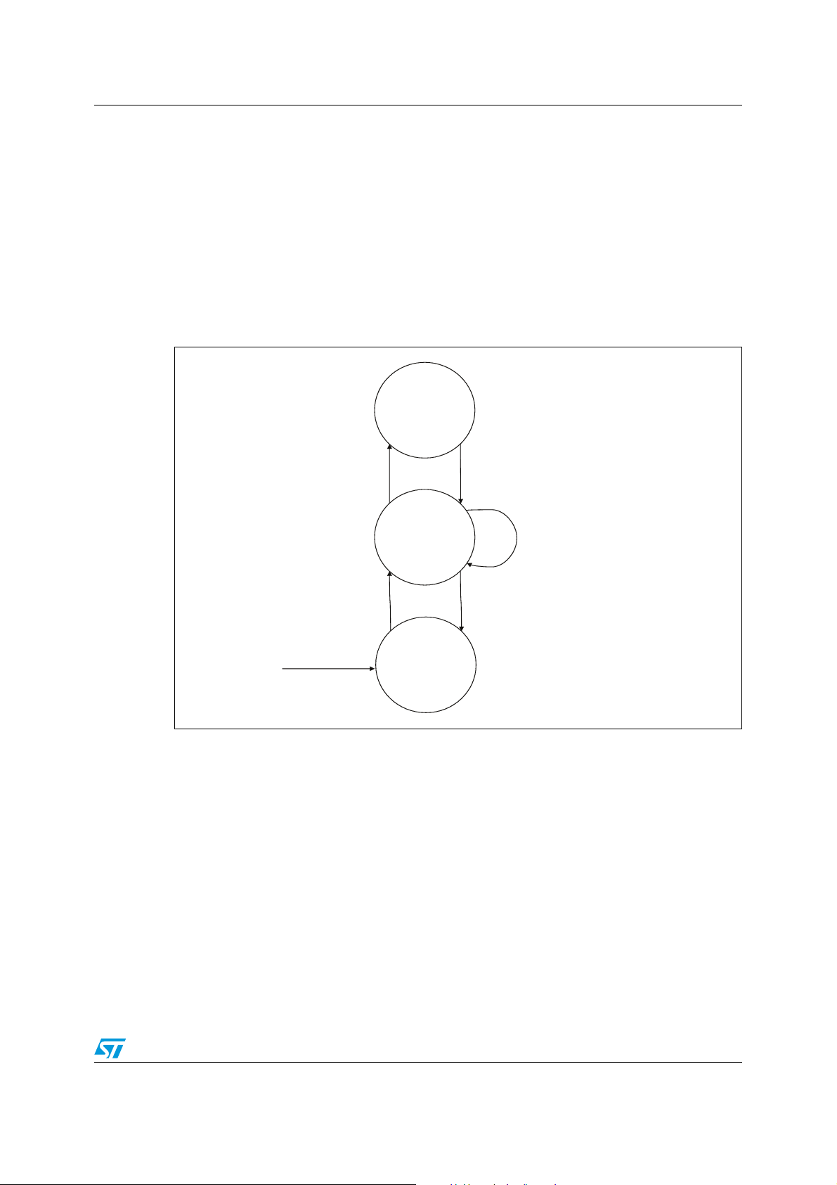
6.1 Operating modes.
The SPV1020 works between three operating modes or states, depending on the voltage
provided by the supply source and by the previous mode or state:
● OFF-state
● Burst mode
● Normal (or MPPT) mode.
Figure 12. SPV1020 general FSM (finite state machine)
Normal/MPPT
Mode
6.2 OFF-state
The SPV1020 has a UVLO (undervoltage lockout) with hysteresis of 500 mV. The two
thresholds are 6.5 V (UVLO_H) for turn-on and 6.0 V for turn-off (UVLO_L).
At power-up, while the supply source provides a voltage lower than UVLO_H, the SPV1020
stays in the OFF-state. In this state, no switching is applied to the switching elements and all
the current provided by the PV panel (supply source) is directly transferred to the output
node through the intrinsic diode of the synchronous rectifiers.
All 4 Phases ON
[VCC > UVLO_H]
POWER UP
Burst
Mode
OFF State
[VCC < UVLO_L]
Not all phases ON
&
Default < N < Max
[VCC < UVLO_L]
&
N = default
AM02599v1
When the applied voltage reaches UVLO_H, the SPV1020 goes into burst mode. Burst
mode guarantees a soft startup and shutdown. When in burst mode, the SPV1020 updates
an internal counter according to the comparison between the sampled supply voltage and
UVLO thresholds. The SPV1020 goes back into the OFF-state when the internal counter
returns to its default value.
Doc ID 018749 Rev 1 15/57
SPV1020 functions AN3392
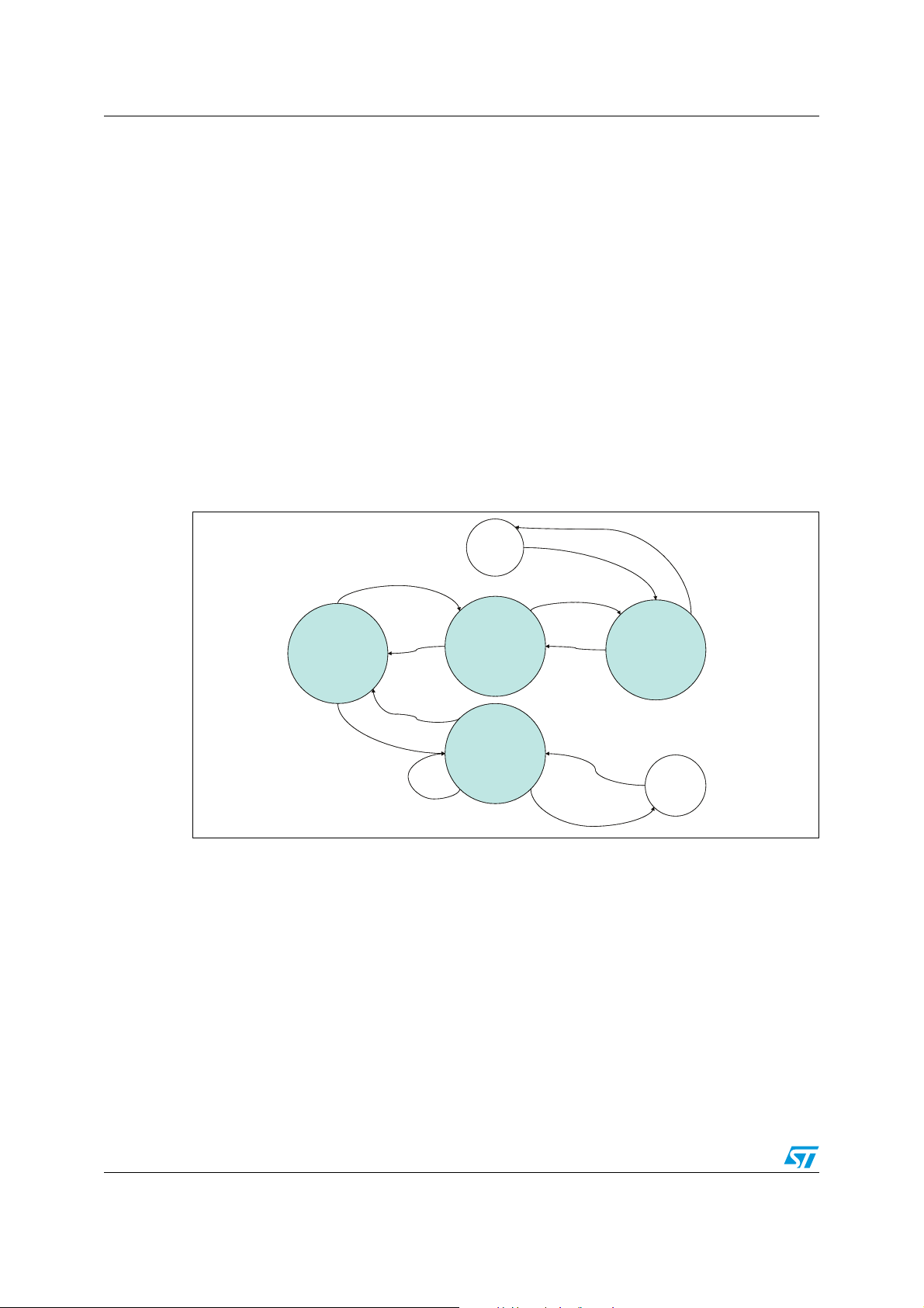
6.3 Burst mode
This mode guarantees a correct startup for the SPV1020, avoiding voltage oscillations. After
the input voltage is applied, the converter begins operation when the input voltage exceeds
6.5 V (ULVO_H).
Burst mode contains four internal states, which guarantee to gradually activate phase “1”
and sequentially the four phases. Figure 13 shows the FSM of burst mode (the grey circles
are the burst mode states).
Each phase is driven with a set of 10 “pulses”. Each pulse can be “ON”, driving the phase
with a signal at a minimum PWM duty cycle of 5%, or “OFF”, with the driving signal
completely low.
When activated, a phase is driven with 1 pulse “ON” and 9 pulses “OFF”. The number of
“ON” pulses can be increased up to 10 (in this case, another phase is activated), or
decreased down to 0 (the phase is always OFF).
An increase or decrease of “ON” pulses depends on the status of the ULVO signal that
checks if the input voltage is greater than the minimum threshold or not.
Figure 13. Burst mode FSM
[UVLO is ON ]
[UVLO is ON ]
Normal
Mode
[UVLO is OF F]
[UVLO is ON ]
Phases 1 & 3 active
@DC=5%
[UVLO is OF F]
[Check UVLO]
When all four phases are active, the system enters normal (or MPPT) mode.
6.4 Normal/MPPT mode
This mode guarantees the maximum power extraction from a photovoltaic input supply by
executing an MPPT algorithm.
The MPPT algorithm generates a voltage reference (Vref) for a PWM generator. The
resulting waveform, with a duty cycle (DC) proportional to Vref, drives the eight internal
switching elements.
[UVLO is OF F]
[UVLO is ON ]
& [n is 10]
Phases 1, 3 & 2 active
@DC=5%
Only Ph ase “1” is active
•n pulses @DC=5%
• (10-n) pulses @DC=0%
If UVL O is ON [n = n+1]
else [n = n -1]
[UVLO is OF F]
[UVLO is OF F]
&
[n is 1]
Phases 1, 3, 2 & 4 active
[UVLO is ON ]
@DC=5%
OFF State
[n = 1]
AM02600v1
16/57 Doc ID 018749 Rev 1
AN3392 SPV1020 functions
Figure 14. SPV1020 MPPT block
VOUT
PV+
PV-
MPPT
VREF
PWM
GEN
VOUT
DC
PV-
PV+
SHIFTING
AM02601v1
This application is equivalent to matching the impedance of the output load to the
impedance of the input source (PV panel). The value of the impedance (Z) that matches the
impedance of the input source depends on the duty cycle (DC) set by the SPV1020.
Figure 15. SPV1020 equivalent circuit
SPV1020
in
I
in
C
in
V
gm Vin
C
out
I
out
R
out
V
out
PV
DC
Panel
Z
AM02602v1
Each Z affects the power transfer between the input source and output load, and for each Z
an input voltage (V
algorithm is to regulate the proper DC in order to guarantee Z = Z
impedance of the source and Z is the impedance assuming Z
which the power extracted from the supply source (P
) and current (Iin) can be measured. The purpose of the MPPT
in
= Vin * Iin) is maximum
in
, where ZM is the
M
as the impedance value for
M
(MPP = VMP * IMP).
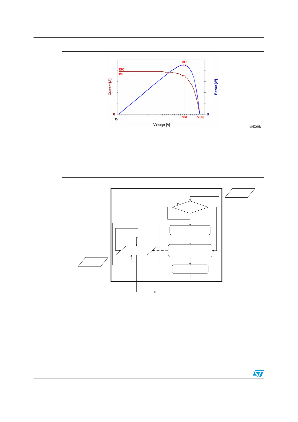
Figure 16 shows both the typical curves, power vs. voltage and current vs. voltage of a
photovoltaic panel.
Doc ID 018749 Rev 1 17/57
SPV1020 functions AN3392
Figure 16. PV panels, power vs. voltage and current vs. voltage curves
The voltage-current curve shows all the available working points of the PV panel at a given
solar irradiation. The power-voltage curve is derived by the voltage-current curve, plotting
the product V*I for each voltage applied.
Figure 17 shows the dataflow diagram of the MPPT algorithm implemented by the
SPV1020:
Figure 17. MPPT data flow diagram
MPPT algorithm
P(tn)
FV
P(tn) > P(t
)
n-1
Output voltage monitoring
V
o-max
V
o-th
V
ref
Sign = Inv(Sign)
V
=
ref
V
+ Sign * Step
ref
Vo (tn)
Update P(t
to DAC
The voltage reference generated by the MPPT algorithm is always limited by the overvoltage
(V
This algorithm is defined as Perturb&Observe because the system is excited (perturbed)
with a certain duty cycle (DC), the power is then monitored (observed), and then perturbed
with a new DC depending on the monitoring result.
) and voltage regulation (V
o-max
) control of the output.
o-th
)
n-1
AM02604v1
The SPV1020 executes the MPPT algorithm with a period equal to 256 times the switching
period. The switching period is 10 µs, therefore the MPPT algorithm period is 2.56 ms. This
time is required for the application to reach the new steady-state (voltage and current) after
18/57 Doc ID 018749 Rev 1

AN3392 SPV1020 functions
the perturbation of the DC. The resolution of the duty cycle perturbation is 0.2 % over most
of its range.
An increase or decrease of the DC depends on the update done in the previous step and by
the direction of the input power.
The MPPT algorithm compares the current input power (P
in the previous step (P
). If the power is increasing then the update is in the same
tn-1
) with the input power computed
tn
direction as in the previous step. Otherwise the update is swapped (from increasing to
decreasing or vice-versa).
When the system is at the MPP, the user can see the duty cycle oscillating between three
values within a time window of 256*3 = 768 times the switching period (7.68 ms).
Figure 18 shows the sampling/working points (red circles) set by the SPV1020 and how they
change (red arrows) during normal operating mode.
Figure 18. MPPT concept flow diagram
The input for the MPPT algorithm is the incoming power but its computation depends on the
working mode of the application, either DCM or CM.
The SPV1020 discriminates between DCM and CM by the zero crossing blocks (ZCB), refer
to Section 3 (Figure 9) for details.
The SPV1020 moves between DCM and CM states implementing a sort of hysteresis,
depending on how many of the four ZCBs (Figure 9) have their own outputs activated.
Figure 19 shows the related finite state machine (FSM) implementation within the
normal/MPPT mode:
Doc ID 018749 Rev 1 19/57

SPV1020 functions AN3392
Figure 19. Normal/MPPT mode, DCM vs. CM FSM
OR:#"ACTIVE
OR:#"ACTIVE
#-
$#-
OR:#"ACTIVE
OR:#"ACTIVE
!-V
In the case of DCM, input current can be negligible and its sampled value may be strongly
affected by the noise caused by the switching elements. Input power is computed as follows,
avoiding the use of the input current:
Equation 4
P
tn()
V2T
on
TonT
+()⋅⋅=
off
In the case of CM, input power is computed by multiplying the sampled voltage and the
sampled current:
Equation 5
tn()
VI⋅=
P
Input voltage is sampled by an external resistive divider, while the input current is sampled
internally to reduce the number of external components in the application. Figure 20 shows
a simple schematic of the input voltage sensing circuitry (see Section 10 for values of the
components shown).
20/57 Doc ID 018749 Rev 1

AN3392 SPV1020 functions
Figure 20. Input voltage partitioning, sample circuit
PV+
PV
Panel
PV -
To LX
D4
C5
To SPV1020 supply (Vin)
R1
C9
To SPV1020 voltage sense (Vin_sns)
To SPV1020 voltage sense ref (Vin_sns_m)
AM02607v1
Doc ID 018749 Rev 1 21/57

Voltage regulation AN3392
7 Voltage regulation
In order to protect both the device itself and the load, the SPV1020 implements a dual
control of the output voltage (V
Control of V
is done through the V
OUT
(see Section 10 for resistance values). The control consists of comparing V
two internal thresholds:
1. 1.00 V, for voltage regulation
2. 1.04 V, for overvoltage protection.
OUT
).
OUT_SNS
pin, connected to V
by a resistive divider
OUT
OUT_SNS
with
When V
OUT_SNS
increases up to 1 V, the output feedback loop enters regulation, limiting the
output voltage. Regulation is achieved by creating an upper limit for the DC generated by the
MPPT algorithm.
The stability of the loop must be externally compensated by connecting a resistor and a
capacitor (pole-zero combination) between the PZ_OUT pin and SGND pin (see Section 10
for values).
7.1 Overvoltage protection
If the V
OUT_SNS
controller which stops the drivers and produces a fault, setting the bit OVV in the status
register. This information is accessible through the SPI interface by the Read Status
command (op code 0x07). When V
converter is switched ON again and the converter restarts the MPP search from the
minimum duty cycle (5 %).
exceeds 1.04 V, a fault signal is generated and transmitted to the fault
OUT_SNS
7.2 Overcurrent protection
To guarantee the safety of the entire application, the SPV1020 implements an overcurrent
protection on the low-side power switches. In fact, when Lx is accidentally shorted to V
V
, or when the current flowing through the inductor exceeds the peak current limit
OUT
(4.5 A), the related low-side power switch is immediately turned OFF and the linked
synchronous rectifier is enabled to turn on. The low-side power switch is turned on again at
the next PWM cycle.
drops back down to 1.04 V the DC-DC
in
or
In the case of overcurrent on branch x [x = 1..4], the related OVC bit of the status register is
set. This information is accessible through the SPI interface by the Read Status command
(op code 0x07).
7.3 Current balance
Different parasitic resistances between the four branches of the IL-4 architecture can be the
root cause of unbalanced current flow between the four branches. This should be avoided
as it may result in lower efficiency or damage to external components (inductors) and/or the
SPV1020.
It is recommended that the four branches in the PCB layout have symmetrical paths and the
inductors be matching or from the same production lot.
22/57 Doc ID 018749 Rev 1

AN3392 Voltage regulation
The SPV1020 implements an internal control guaranteeing the current balance between the
four branches, monitoring the current flowing on each branch with a maximum variation of
350 mA.
7.4 SPI serial peripheral interface
The SPV1020 implements a 4-pin compatible SPI interface. The SPI allows full duplex,
synchronous, serial communication between a host controller (the master) and the
SPV1020 peripheral device (the slave). The SPV1020 provides the following 4 pins:
● XCS (or SS)
● SPI_CLOCK (or SCLK)
● SPI_DATA_IN (or MOSI)
● SPI_DATA_OUT (or MISO).
Figure 21. SPI interface: master/slaves connection example
The SPI master selects one of the slaves, provides the synchronizing clock and starts the
communication. The idle state of the serial clock for the SPV1020 is high, while data pins
are driven on the falling edges of the serial clock and are sampled on its rising edges (SPI
control bits CPOL = 1, and CPHA = 1). The bit order of each byte is MSB first.
When the master initiates a transmission, a data byte is shifted out through the MOSI pin to
the slave, while another data byte is shifted out through the MISO pin to the master; the
master controls the serial clock on the SCLK pin. The SS (active low) pin must be driven low
by the master during each transmission.
Doc ID 018749 Rev 1 23/57

Voltage regulation AN3392
Figure 22. Frame structure: register read operation
The SPV1020 register file is accessible by the host through the SPI bus. Therefore, the host
can read some registers of the SPV1020 control parameters. Each data frame includes at
least one command byte followed by some data bytes whose direction depends on the type
of command. If the command byte requires some data to be read from the register file, those
data are transmitted from the slave to the master through the MISO pin; therefore the master
appends a number of NOPs (0x00) to the command, so that the entire data can be
transmitted, see Figure 22. In other words, the master must transmit a byte to receive a byte.
If the SS wire goes high before the completion of a command byte in the data frame, the
SPV1020 rejects that byte and the frame is closed; then the next data frame is considered
as a new one, starting with a command byte.
Some data words can be longer than 8 bits, such as ADC results (10 bits); in such cases,
data is first extended to the nearest multiple of one byte (it is right justified), then it is split
into bytes, e.g. the ADC result R is formatted as follows:
Table 1. Data format for words longer than 8 bits
Bit 7
MSB
Byte 1000000
Byte 2R7R6R5R4R3R2R1
Bit 6 Bit 5 Bit 4 Bit 3 Bit 2 Bit 1
R9
MSB
Bit 0
LSB
R8
R0
LSB
24/57 Doc ID 018749 Rev 1

AN3392 Voltage regulation
Ta bl e 2 shows a list of commands. Each command addresses a memory location of a
certain width and sets the direction of the related data.
Table 2. Commands list
Code (Hex) Name R/W Comment
00 Reserved Reserved
01 NOP No operation
02 SHUT Shuts down SPV1020
03 Turn-on Required only after SHUT command
04 Read current Read Read 10 bits in 2 bytes (MSB is first received bit)
05 Read vin Read Read 10 bits in 2 bytes (MSB is first received bit)
06 Read pwm Read Read 9 bits in 2 bytes (MSB is first received bit)
07 Read status Read
Read 7 bits:
OVC (4bits), OVV (1bit), OVT (1bit), CR (1bit)
For further information on the SPI interface, such as timing diagrams, please refer to the
SPV1020 datasheet.
Doc ID 018749 Rev 1 25/57

Pin description AN3392
8 Pin description
Table 3. Pin description
Pin
(PSSO-36)
34 V
Name Type Description
in
Supply DC input power
Boost output voltage, pins 7 and 8 are internally shorted and connected
7,8,17,18,19,
20,29,31
V
OUT
Supply
to pins 29 and 30.
Pins 17 and 18 are internally shorted and connected to pins 19 and 20.
All of the V
pins must be connected to the V
OUT
rail of the PCB.
OUT
12,13,24,25 PGND Ground Power ground to be connected to the ground plane of the PCB.
1 SGND Ground Signal ground to be connected to the ground plane of the PCB.
10,11,14,15,
22,23,26,27
9,16,21,28 CB1…4 I/O
LX1…4 I Boost inductor connection.
External bootstrap capacitors to be connected between these pins and
LXi.
Chip select for SPI interface:XCS = HIGH => SPI device is not active
31 XCS I
XCS = LOW => SPI device is active
If this pin is left floating an internal resistor pulls the XCS pin up,
switching the SPI off.
32 SPI_DATA_IN I
33 SPI_CLK I
Input pin for SPI data flow. If not used, this pin should be connected to
ground.
Input pin for SPI clock signal. If not used, this pin should be connected to
ground.
35 VIN_SNS I
Sense pin of input voltage. To be biased with a resistor divider between
VIN and SGND.
36 VIN_SNS_M I Dedicated reference pin for voltage sensing.
2PZ_OUTI/O
3V
OUT_SNS
This pin is used to compensate the feedback loop of the output voltage.
A series of resistors and capacitors must be connected to SGND.
Sense pin of output voltage. To be biased with a resistor divider between
I
V
OUT
and SGND.
Pin for adjusting the switching frequency. To set the default value (100
4OSC_INI
kHz) this pin must be tied to VREG, otherwise for adjustment it must be
biased through a resistor to SGND.
5VREGI/O
Power supply for internal low-voltage circuitry; an external capacitor
must be connected from this pin to the ground plane of the PCB.
6 SPI_DATA_OUT O Output pin for SPI data flow. If not used, this pin should be left floating.
26/57 Doc ID 018749 Rev 1

AN3392 Pin description
28
CB2
CB4
9
8.1 Pin connection
Figure 23. Pin connection top view PowerSSO-36
19
20
21
22
23
24
25
26
27
29
30
31
32
33
34
35
36
VOUT
VOUT
CB1
LX1
LX1
PGND
PGND
LX2
LX2
VOUT
VOUT
XCS
SPI_DATA_OUT
SPI_DATA_IN
SPI_CLK
VIN
VIN_SNS
VIN_SNS_M
VOUT
VOUT
CB3
LX3
LX3
PGND
PGND
LX4
LX4
VOUT
VOUT
VREG
OSC _IN
VOUT_SNS
PZ-OUT
SGND
18
17
16
15
14
13
12
11
10
8
7
6
5
4
3
2
1
Doc ID 018749 Rev 1 27/57

Absolute maximum ratings AN3392
9 Absolute maximum ratings
Table 4. Maximum ratings
Symbol Parameter
V
V
in
OUT
Power supply [-0.3, 40] V
Power supply [-0.3, 40] V
Range
[min., max.]
Unit
PGND Power ground 0 V
SGND Signal ground [-0.3, 0.3] V
V
OUT_SNS
LX1….4 Analog input [-0.3, V
Analog input [-0.3, V
+ 0.3] V
out
+ 0.3] V
out
CB1…4 Analog input/output [Lxi – 0.3, Lxi + 5] V
VREG Analog input/output [-0.3, 6] V
VIN_SNS Analog input [-0.3, 3.3 + 0.3] V
XCS Digital input [-0.3, 3.3 + 0.3] V
OSC_IN Analog input [-0.3, 3.3 + 0.3] V
PZ_OUT Analog input/output [-0.3, VIN + 0.3] V
SPI_DATA_OUT Analog output [-0.3, 3.3 + 0.3] V
SPI_CLK Digital input [-0.3, 3.3 + 0.3] V
SPI_DATA_IN Digital input [-0.3, 3.3 + 0.3] V
VIN_SNS_M Dedicated ground [-0.3, + 0.3] V
28/57 Doc ID 018749 Rev 1

AN3392 External component selection
10 External component selection
The SPV1020 requires a set of external components and their proper selection guarantees
both the best chip functionality and system efficiency.
The following sections refer to the connections and component labels shown in Figure 24
below:
Figure 24. STEVAL-ISV009V1 schematic (PowerSSO-36 package)
J47
J47
FASTON
L52u5H L52u5H
D2
C15 4.7uFC15 4.7uF
C6 4.7uFC6 4.7uF
100nFC4100nF
C8 22nFC8 22nF
C4
C7 470nFC7 470nF
0
FASTON
J48
J48
FASTON
FASTON
L347uH L347uH
OSC_IN
L447uH L447uH
4
123
123
4
VIN3L3L
R7 dnmR7 dnm
Vout+
Vout-
VOUT_SNSVOUT_SNS
VIN4L4L
C10
C10
220pF
220pF
V_OUT
R3
3.9MR33.9M
1 2
R4
110kR4110k
1 2
0
0
D1 SPV1001N40D1 SPV1001N40
V_OUT
C134.7uF C134.7uF
C124.7uF C124.7uF
D5
TP5
TP5
1
PV+_1
PV+_1
D6
SPV1001-N30D6SPV1001-N30
TP6
TP6
1
PV-_1
PV-_1
D7
SPV1001-N30D7SPV1001-N30
TP7
TP7
1
PV+_1
PV+_1
D8
SPV1001-N30D8SPV1001-N30
TP8
TP8
1
PV-_1
PV-_1
VIN
J40
J40
CONN FLEX 2
CONN FLEX 2
D3STPS160UD3STPS160U
VCC
C11
C11
1uF
1uF
VIN
PV+
D4
1
SMB36CAD4SMB36CA
2
PV-
R1
3.3MR13.3M
1 2
C5
VIN_SNSVIN_SNS
4u7FC54u7F
0
R2
110kR2110k
1 2
VIN_SNS_M
0
J36
J36
C9
220pFC9220pF
4 HEADER
4 HEADER
VIN L2
C1 100nFC1 100nF
L1 47uHL1 47uH
V_OUTV_OUT
C16 4.7uFC16 4.7uF
C2
100nFC2100nF
V_OUT
L1
L2
SHUT/SPI_XCS
TEST_DATA/SPI_DATA_IN
TEST_CLK/SPI_CLK
VIN_SNS_M
0 0
C14 4.7uFC14 4.7uF
1
2
3
4
DIAG/SPI_DATA_OUT
L2 47uHL2 47uH
CB1CB1CB1CB1CB1
L1VIN
20
21
CB1
22
23
24
25
26
27
28
CB2
29
30
31
32
33
34
VCC
35
VIN_SNS
36
SPV1020 (PSSO36 package)
SPV1020 (PSSO36 package)
CB2CB2CB2CB2CB2
SMB36CAD5SMB36CA
J35
J35
00
1819
17
16
15
14
13
12
11
10
9
8
7
6
5
4
3
2
1
CB3CB3CB3CB3CB3
V_OUT
CB3
PGNDPGND
CB4
Vreg
OSC_IN
VOUT_SNSVOUT_SNSVOUT_SNSVOUT_SNS
PZ_OUT
AGND
CB4CB4CB4CB4CB4
SPV1001N40D2SPV1001N40
L3
L4
V_OUT
DIAG/SPI_DATA_OUT
R6 0R6 0
R5 1kR5 1k
C3 100nFC3 100nF
High Current Path Legend
Iin path
Iout path
Ground path
ST SOLAR KEY PRODUCT Legend
SPV1001-N30 SPV1001-N40 SPV1020
Please note the connections to OSC_IN are alternative connections. For the default
switching frequency of 100 kHz, connect OSC_IN to VREG. For frequencies other than 100
kHz, connect a resistor between OSC_IN and SGND (see Section 10.11).
Doc ID 018749 Rev 1 29/57

External component selection AN3392
10.1 Power and thermal considerations
The SPV1020 performance is strongly impacted by the power capability of the PowerSSO36 package, as well as the application board. According to the technical note TN0054,
R
“2s2p” multi-layer board with thermal vias and a metal plate for an external heatsink.
of the PowerSSO-36 can be decreased to 10 °C/W if the package is soldered onto a
TH(j-a)
Starting from this value, it is possible to calculate the P
Equation 6
TJT
AMBRTH j a–()PD
Equation 7
1 η–()P
⋅=
MAX
The SPV1020 efficiency (
η ) is ≥ 98%; the thermal shutdown threshold is 140 °C;
typical ambient temperature (T
P
D
) for a photovoltaic application is 85 °C.
AMB
Calculating maximum power dissipation Pd:
Equation 8
TJT
–
AMB
------------ ------------
P
D
R
TH j a–()
5.5W==
Equation 9
P
D
P
MAX
--------------- -
1 η–()
275W==
MAX
⋅+=
.
If the package is soldered onto a “2s2p” multi-layer board with thermal vias, the R
20 °C/W and then P
is 138 W. (PCB with 4 layers: 2 soldered layers, top and bottom,
MAX
and 2 power layers (inner layers for power dissipation).
10.2 Inductor selection
Inductor selection is a critical element for this application.
Inductor selection must take into account the following application conditions:
● Maximum input current (i.e. Imp and Isc of the PV panel)
● Maximum input voltage (i.e. Vmp and Voc of the panel)
● Overcurrent threshold of the SPV1020
● Maximum duty cycle, according to maximum output voltage
Input current from the PV panel is split between the 4 inductors of each branch, so:
Equation 10
I
mp
rms()
I
Lx
30/57 Doc ID 018749 Rev 1
------- -
is
TH(j-a)
I
sc
------
<≅
4
4

AN3392 External component selection
According to Figure 6, during the charge phase (switch ON), peak current on each inductor
depends on the applied voltage (V
), on the inductance (Lx) and on the time (TON).
in
Equation 11
1
Vmp
-------------
ILxpk()ILxrms()
-- -
⋅⋅+≅
2
T
L
ON
x
Taking into account the overcurrent threshold (4.5 A):
Equation 12
A5.4)pk(I
<
Lx
Finally, inductance should be chosen according to the following formula:
Equation 13
×
V
1
mpTON
----------- ------------- ----------- --
---
L
x
4.5 I
2
Lx
rms()–
1
-- -
2
V
mpTON
------------ ------------ -----
×=⋅>
4.5
⋅
I
mp
--------–
4
Considering the possible unbalance of the currents and the inductance drop due to self
heating effect, a more conservative choice would be to replace 4.5 A with 3.15 A (70%).
Triggering the overcurrent threshold will cause limitation of the duty cycle and consequently
limitation of the input and output powers.
Usually, inductances ranging between 22 µH to 100 µH satisfy most application
requirements.
Critical parameters for the inductor choice are inductance (analyzed above), Irms current,
saturation current, and size.
The current flowing through an inductor causes its internal temperature increase (selfheating effect). Irms typically indicates the current value causing a temeprature increase of
20, 30, or 40 °C. The higher the temeprature, the higher the inductance drop with respect to
its nominal value.
For the same physical size, smaller inductance values provide for faster response to load
transients and higher efficiency. Inductor size also affects the maximum current deliverable
to the load. The saturation current of the inductor should be higher than the peak current
limit of the input source. The suggested saturation current should be > 4.5 A.
Inductors with low series resistance are suggested to guarantee high efficiency.
10.3 Bootstrap capacitors
C1, C2, C3, and C4 are four capacitors used to guarantee internal functionality of the
SPV1020. Their role is to maintain the required voltage level on pins CB1, CB2, CB3, and
CB4 even during the charging phase of the inductors.
Capacitance value is the same for all four capacitors and is not application dependant. The
suggested value is in the range of 22 nF to 100 nF. Each capacitor switches synchronously
with the related inductor (at 100 kHz). The maximum voltage is fixed by the internal voltage
regulator (~5 V).
Doc ID 018749 Rev 1 31/57

External component selection AN3392
Low ESR capacitors are a good choice to increase the entire system efficiency.
10.4 Internal voltage rail capacitors
C7 is a tank capacitor used to guarantee the voltage level (5 V) of the internal SPV1020
voltage regulator.
The suggested value is 470 nF and is not application dependent.
The voltage range is the same as for the boost capacitors. Maximum voltage must be higher
than 5 V.
Low ESR capacitors are recommended in order to increase the entire system efficiency.
10.5 Input voltage capacitors
C5 is the input capacitance added at the input to reduce the voltage ripple.
The maximum voltage of this capacitor is dependent upon the input source (typically
between 25 V and 50 V).
Low-ESR capacitors are recommended in order to increase the whole system efficiency.
Suggested minimum input capacitance is 2 µF.
In order to reduce the ESR effect, it is suggested to split the input capacitance into 2
capacitors connected in parallel.
Another capacitor (C11) is connected to the supply input pin of the SPV1020 (V
to stabilize the voltage as much as possible on this pin which may be affected by the ripple
of the PV panel voltage.
Considering the maximum current (Isc) provided by the PV panel connected at the input, the
following formula can be used to select the proper capacitance value (Cin) for a specified
maximum input voltage ripple (V
in_rp_max
Equation 14
Cin
10.6 Input voltage partitioning
The input voltage must be scaled to the reference voltage (1.25 V) of the ADC integrated in
the SPV1020.
R1 and R2 are the 2 resistors used for partitioning the input voltage.
When the the open circuit voltage (Voc) of the PV panel is known, the said R1 and R2 must
be selected according to the following rule:
):
I
sc
------------ ------------- ----------- -------
≥
V
in_rp_maxFsw
⋅
). Its role is
in
Equation 15
V
R1
------- -
R2
32/57 Doc ID 018749 Rev 1
oc
----------- 1–=
1.25

AN3392 External component selection
In order to optimize the efficiency of the entire system, the selection of R1 and R2, should
take their power dissipation into account.
Assuming negligible the current flowing through pin VIN_SNS, maximum power dissipation
of the series R1+R2 is:
Equation 16
P
vin_sns
=
------------ ----------
R1 R2+
Voc()
2
Empirically, R1 and R2 should be selected according to:
Equation 17
P
vin_sns
1% V
in_maxIin_max
⋅()«
Note: In order to guarantee the proper functionality of pin VIN_SNS, current flowing in the series
R1+R2 should be in the range between 20 µA and 200 µA.
10.7 Input voltage sensing capacitor
C9 is placed in parallel with R2 and as close as possible to pin VIN_SNS.
Its role is to stabilize as much as possible the voltage sensed by pin VIN_SNS.
Critical parameters for the capacitor are: capacitance, maximum voltage, and ESR.
Maximum voltage: if R1 and R2 have been properly chosen, to partition V
the maximum voltage of this capacitor can be in the range from 3.3 V or higher.
The capacitance value depends on the time constant (τ
C6*R1//R2) and by the system switching frequency (F
) composed with R1+R2 (τin=
in
= 4*FSW).
SSW
Assuming R1 >> R2 (so, R1//R2 ~= R2):
Equation 18
1
----------- -
10
τ
⋅≅
in
F
ssw
to 1.25 V, then
in
so,
Equation 19
C9 10
Note: Even if the SPV1020 controls each phase at F
frequency (F
) is four times the single-phase switching frequency (by default 400 kHz).
SSW
10.8 Output voltage capacitors
A minimum output capacitance must be added at the output, in order to reduce the voltage
ripple.
Doc ID 018749 Rev 1 33/57
1
⋅⋅≅
------------
F
SW
1
------- -
R2
ssw
(by default 100 kHz), the system switching

External component selection AN3392
Critical parameters for capacitors are: capacitance, maximum voltage and ESR.
Maximum voltage of this capacitor is strictly dependent upon the output voltage range. The
SPV1020 can support up to 40 V. The minimum suggested voltage for these capacitors is
50 V.
Low ESR capacitors are a good choice in order to increase the entire system efficiency.
The suggested minimum output capacitance is 28 µF. In the case of series connection (see
Appendix B: SPV1020 parallel and series connection), it is suggested to increase the output
capacitance up to 100 µF.
In order to reduce the ESR effect it is suggested to split the output capacitance into three
capacitors connected in parallel.
In accordance with the maximum current (Isc) provided by the PV panel connected at the
input, the following formula can be used in order to select the proper capacitance value
(Cout) for a specified maximum output voltage ripple (V
out_rp_max
):
Equation 20
I
------------- ------------- ---------- ----------
C
≥
out
V
sc
out_rp-maxFSW
⋅
It is suggested to split the capacitance into four capacitors, each to be connected to each of
the four V
pins of the SPV1020. This helps to balance the impedance of the four tracks.
OUT
10.9 Output voltage partitioning
R3 and R4 are the two resistors used for partitioning the output voltage.
If V
OUT_MAX
according to the following rule:
Equation 21
Also, in order to optimize the efficiency of the entire system, when selecting R3 and R4, their
power dissipation must be taken into account.
Assuming negligible current flowing through pin V
the series connection of R3 and R4 is:
Equation 22
Empirically, R3 and R4 should be selected according to:
Equation 23
is the maximum output voltage at the load, then R3 and R4 must be selected
R3
------- -
R4
P
vout_sns
P
vo u t _sns
V
out_max
------------- --------- 1–=
1.00
V
()
out_max
------------- ------------- - -
=
R3 R4+
1% V
out_maxIou t_max
OUT_SNS
2
⋅()«
, maximum power dissipation in
34/57 Doc ID 018749 Rev 1

AN3392 External component selection
Note: In order to guarantee the proper functionality of V
connection of R3 and R4 should be between 20 µA and 200 µA.
10.10 Output voltage sensing capacitor
C10 is placed in parallel with R4 and is as close as possible to V
Its role is to maximize the stability of the voltage sensed by the V
If R3 and R4 are chosen properly and partition V
capacitor can be 3.3 V or higher.
The capacitance value depends on the time constant (τ
C8*R3//R4) and by the system switching frequency (F
Assuming R4<<R3 (so, R3//R4
Equation 24
so,
Equation 25
≅ R4):
T
C10 10
OUT
10
⋅⋅≈
------------- - -
F
SSW
OUT_SNS
OUT
----------- -
⋅≈
F
1
current flowing in the series,
OUT_SNS
OUT_SNS
.
pin.
to 1.25 V, the voltage rating of this
) composed with R4 (τ
out
1
ssw
SSW
1
------- -
R4
= 4*F
SW)
.
out
=
Note: Even if the SPV1020 controls each phase at F
switching frequency (System-Fswitch) is four times the single-phase switching frequency (by
default 400 kHz).
10.11 Internal oscillator frequency
The SPV1020 controls the boost application by a PWM signal operating at the default
switching frequency of 100 kHz.
Default switching frequency is guaranteed by connecting the OSC_IN pin to 5 V (VREG).
The user can change the default value by placing a proper resistor (R6), as shown in
Figure 24, to ground.
The internal oscillator works with an integrated resistor of 120 kΩ. Frequency is proportional
to the current provided to the oscillator block.
To change F
following formula:
Equation 26
to the desired switching frequency, R7 must be selected according to the
switch
R7 kΩ[]
(by default 100 kHz), the entire system
SW
100()120()⋅
------------ ------------ ----------- - -=
F
switch
kHz[]
Doc ID 018749 Rev 1 35/57

External component selection AN3392
10.12 Diode selection
The SPV1020 requires 3 Schottky diodes: D1, D2 and D3, as shown in Figure 24.
D3 (with C11) protects the SPV1020 supply by filtering system switching noise.
D3 should be chosen for low forward drop so that it doesn’t impact system efficiency.
Maximum forward current is according to the maximum current required by the SPV1020. A
safe choice is around 20 mA. Maximum voltage applied to D3 depends on the PV panel, and
does not exceed 45 V due to the maximum allowable SPV1020 input voltage.
D1 is the alternative path for current flow when the SPV1020 is down and V
V
.
OUT
D2 is a bypass diode. It turns on in the case of shaded cells and provides an alternative path
for the current flowing from other panels.
D1 and D2 are power Schottky diodes that must support both:
● Forward current comparable with the maximum current provided by the PV cells.
Assuming a PV panel with 6” poly crystalline silicon solar cells, then the maximum
current is 9 A.
● Maximum reverse voltage according to the output voltage partitioning. This should be
at least 45 V due to the voltage rating of the SPV1020.
Furthermore, the forward voltage and reverse current of D1 and D2 should be as low as
possible in order to minimize the impact on system efficiency.
10.13 Protection devices
The SPV1020 demo board uses a protection Transil™ D4 to trigger voltage spikes higher
than 45 V (AMR of the SPV102) on the V
This component must be chosen according to the following rules:
VBR > V
and
OUT
_max;
OUT
pins.
is higher than
in
VCL
≤ 45 V.
The STEVAL-ISV009V1 uses D4 which has VBR = 37 V and VCL = 40 V.
10.14 Pole-zero compensation
The SPV1020 controls the whole system stability by an internal loop on V
The transfer function of the loop depends on both the output capacitor and load.
Even though the stability can be fine tuned by trimming R5 and C8 on pin PZ_OUT, as
shown in Figure 24, their suggested values (R5 = 1 kΩ and C8 = 22 nF) guarantee stability
in most applications.
In order to increase system response to output voltage changes without causing overvoltage
threshold triggering, C8 can be decreased down to 2.2 nF.
36/57 Doc ID 018749 Rev 1
OUT_SNS
.

AN3392 Layout guidelines
11 Layout guidelines
The PCB layout is very important in order to minimize noise, high frequency resonance
problems and electromagnetic interference.
Paths between each inductor and its relative pin must be designed with the same
resistance. Different resistances between the four branches can be the root cause of an
unbalanced current flow among the four branches. Unbalanced currents can cause damage
and a poor tracking of the MPPT.
The same approach must be followed for the four V
It is essential to keep the paths where the high switching current circulates as small as
possible. This reduces radiation and electromagnetic resonance problems.
Large traces for high current paths and an extended ground plane under the metal slug of
the package help reduce noise and heat dissipation (which is strongly impacted by the
thermal vias as well), and also increase efficiency.
Boost capacitors must be connected as close as possible to the Lx and CBx pins.
It is also suggested to connect the bootstrap capacitor directly to the Lx track making sure
there is no voltage drop between the Lx pin and bootstrap capacitor connection due to
current flowing through Lx.
The output and input capacitors should be very close to the device.
The external resistor dividers, if used, should be as close as possible to the VIN_SNS and
V
OUT_SNS
noise pickup.
As an example of a recommended layout, see the demonstration board in Figure 25 and 26:
Figure 25. PCB layout example (top view)
of the device, and as far as possible from high current circulating paths, to avoid
OUT
tracks.
Doc ID 018749 Rev 1 37/57

Layout guidelines AN3392
Figure 26. PCB layout example (bottom view)
38/57 Doc ID 018749 Rev 1

AN3392 Bill of material
12 Bill of material
Ta bl e 5 shows a list of suggested external components to configure the SPV1020 in an
application with V
= 30 V, Imp = 9 A, V
OC
out_max
Table 5. Bill of material
Component Name Value Supplier Serial number
= 36 V and FSW = 100 kHz.
C1, C2, C3,
C4
C11 Die supply capacitor 1 µF Murata EPCOS
C5 PV input capacitor 4.7 µF Murata EPCOS
C9, C10 Voltage sensing capacitors 220 pF Murata EPCOS
C8 Compensation capacitor 22 nF Murata EPCOS
C7 Internal reference voltage capacitor 470 nF Murata EPCOS
C6, C12,
C13, C14,
C15, C16
D3 Decoupling of supply pin STPS160U ST STPS160U
R1 Input voltage partitioning resistor 3.3 MΩ VISHAY D11/CRCW0603 3.3M
R2 Input voltage partitioning resistor 110 kΩ Cyntec RR0816R-114-DN-11
R3 Output voltage partitioning resistor 3.9 MΩ VISHAY D11/CRCW0603 3.9M 1%
R4 Output voltage partitioning resistor 110 kΩ Cyntec RR0816R-114-DN-11
Bootstrap capacitors 100 nF Murata EPCOS
Output capacitors 4.7 µF Murata EPCOS
GRM188R71C104KA01
C1608X7R1H104K
GRM31MR71H105KA88
C3216X7R1H105K
GRM31MR71H475KA88
C3216X7R1H475K
GRM188R71E221KA01
C1608C0G1H221J
GRM188R71C223KA01
C1608X7R1H223K
GRM188R71A474KA61
C1608X7R1C474K
GRM32ER71H475KA88K
C3225X7R1H475K
R5 Compensation resistor 1 kΩ Cyntec RR0816R-102-DN-11
Pull-up resistor
R6
R7
(optional)
L1, L2, L3,
L4
D6, D7, D8 PV panel bypass diodes SPV1001N30 ST SV1001-N30
(Note: R6 must be removed if R7 is
soldered)
Oscillator resistor
(Note: R6 must be removed if R7 is
soldered)
Phase x (x=1..4) inductors 47 µH
Doc ID 018749 Rev 1 39/57
0 Ω
Depending
on desired
F
sw
Cyntec PIMB136T-470MS-11
Coilcraft MSS1278T-473ML
EPCOS
Murata 49470SC
B82477G4473M003
B82477G4473M

Bill of material AN3392
Table 5. Bill of material (continued)
Component Name Value Supplier Serial number
D1, D2 Controller bypass diodes SPV1001N40 ST SPV1001N40
J35 Voltage boost controller SPV1020 ST SPV1020
J36 SPI I/F connector
4-pin
connector
PHOENIX
CONTACT
1723672
D4
J47, J48 Output connector
J40 Alternative input connector
L5 Output current ripple filter 2.5 µH Coilraft MLC1550-252ML
600 W, 40 V bi-directional
protection Transil
SMBJ36CA ST SMBJ36A-TR
FASTON
connector
2-pin
connector
PHOENIX
CONTACT
40/57 Doc ID 018749 Rev 1

AN3392 STEVAL-ISV009V1 application diagram
Appendix A STEVAL-ISV009V1 application diagram
The following figure shows how to connect the STEVAL-ISV009V1 to a photovoltaic panel.
Figure 27. STEVAL-ISV009V1 application schematic
67(9$/,699
3
9
39SDQHO
9RXW
9RXW
3
9
6391
639
6391
It is possible to utilize a PV string by connecting the output stages of the SPV1020 in series
to guarantee the voltage level required by the specific application.
Maximum voltage for the STEVAL-ISV009v1 is 36 V, according to R3/R4 partitioning.
For example, if the application requires 400 V (V
STEVAL-ISV009V1 to be connected in series (Ns_min) is:
Equation 27
V
Ns
_min
out_tot
------------ -----------
V
out_max
In order to guarantee the performance of the whole PV string (e.g. in the case of shaded
panels), a minimum redundancy (10%) on Ns_min is suggested.
Furthermore, considering that the SPV1020 is a voltage boost converter, it is required that
the maximum input voltage (Vo of each PV panel) must be lower than its output voltage. So
the maximum number of devices in series is also limited by the following rule:
) then the minimum number of
out_tot
400
--------- - 12==≥
36
Equation 28
V
out_tot
Ns_max
Doc ID 018749 Rev 1 41/57
------------------ -
≤
V
oc

SPV1020 parallel and series connection AN3392
Appendix B SPV1020 parallel and series connection
The output pins of the SPV1020s can be connected both in parallel and in series. In both
cases the output power (Pout) depends on light irradiation of each panel (Pin), application
efficiency, and on the specific constraint of the selected topology.
The objective of this section is to explain how output power is impacted by the selected
topology.
Examples with three PV panels are presented, but the result can be extended to a larger
number of PV panels.
In the case of the SPV1020 being ON (I.e. there is enough light irradiation so that V
=
in
6.5 V):
Equation 29
Poutx η= Pinx x 1..3=[]
In the case of the SPV1020 being OFF, the system efficiency depends on the drop of the
bypass diode D1 (according to the schematic in Figure 24):
Equation 30
Poutx η
P= inx x 1..3=[]
bp
Finally, in the case of the panel being completely shaded:
Equation 31
Poutx 0=
42/57 Doc ID 018749 Rev 1

AN3392 SPV1020 parallel and series connection
B.1 SPV1020 parallel connection
This topology guarantees the desired output voltage even if only one of the panels is
irradiated. Of course, the constraint of this topology is that V
voltage ratings.
The following figure shows a detail of the parallel connection topology:
Figure 28. SPV1020, output parallel connection
is limited to the SPV1020
OUT
9R
XW
9R
9R
9R
9R
9R
9R
9RXW
".W
39
39
39
39
,69Y
39
39
,69Y
39
39
,69Y
39
The output partitioning (R3/R4) of the three SPV1020s must be in accordance with the
desired V
OUT
.
According to the topology:
Equation 32
Vout Vout1 Vout2 Vout3===
Equation 33
Iout Iout1 Iout2 Iout3++=
According to the light irradiation on each panel (Pin) and to the system efficiency (
power is:
Equation 34
Pout Pout1 Pout2 Pout3===
Equation 35
Poutx Voutx Ioutx x 1..3=[]⋅=
Doc ID 018749 Rev 1 43/57
η), output

SPV1020 parallel and series connection AN3392
Equation 36
Pinx Vinx Iinx X 1..3=[]⋅=
so,
Equation 37
Pout Vout Iout1 Iout2 Iout3++()η Pin1 η Pin2 η Pin3++==
Each SPV1020 contributes to the output power providing Ioutx according to the irradiation of
its panel.
Furthermore, the desired V
is guaranteed if at least one of the 3 PV panels provides
OUT
enough power to turn on the related SPV1020.
B.2 SPV1020 series connection
This topology provides an output voltage that is the sum of the output voltages of each
SPV1020 connected in series. The following shows how the output power is impacted by the
topology.
Figure 29 shows a detail of the series connection topology:
Figure 29. SPV1020, output series connection
06
06
"//34
-004
"//34
-004
6O
UT
06
DISTRIBUTED
ARCHITECTURE
In this case, the topology implies:
Equation 38
Iout Iout1 Iout2 Iout3===
Equation 39
Vout Vout1 Vout2 Vout3++=
44/57 Doc ID 018749 Rev 1
"//34
-004
6O U T
!-V

AN3392 SPV1020 parallel and series connection
In the case where the irradiation is the same for each panel:
Equation 40
Pin1 Pin2 Pin3==
Equation 41
Pout 3 Poutx x 1..3=[]⋅=
Equation 42
1
Poutx
-- -
Pout=
3
Equation 43
Poutx Voutx Ioutx Voutx Iout⋅=⋅=
so,
Equation 44
1
Voutx
For example, assuming Pout = 90 W and, if desired V
-- -
Vout=
3
= 90 V, then Voutx = 30 V.
OUT
Lower irradiation for one panel, for example on panel 2, causes lower output power, so lower
Vout2 due to the Iout constraint:
Equation 45
Poutx
------------ ----=
Iout
The output voltage (V
Voutx
) required by the load can be supplied by the 1st and 3rd SPV1020
OUT
but only up to the limit imposed by their R3/R4 partitioning.
Some examples can help to understand the various scenarios assuming the following
conditions: R3/R4 limiting Voutx = 40 V and desired V
OUT
= 90 V.
Example 1:
Panel 2 has 75% of the irradiation that panels 1 and 3 have:
3
Vout2
-- -
Vout1
4
Pout1 Pout2 Pout3==
3
Pout2
-- -
Pin1 22.5W==
4
3
-- -
Vout3⋅=⋅=
4
Pout Pout1 Pout2 Pout3 82.5W=++=
Doc ID 018749 Rev 1 45/57

SPV1020 parallel and series connection AN3392
Iout
Pout
-------------
Vout
Vout1 Vout3
Vout2
82.5
----------- 0.92A===
90
30
---------- - 32.6V===
0.92
22.5
----------- 24.45V==
0.92
Two of the SPV1020s (1st and 3rd) supply most of the voltage drop due to the lower
irradiation on panel 2.
Note: The SPV1020 is a boost controller, so Voutx must be higher than Vinx, otherwise the
SPV1020 turns off and the input power is transferred to the output stage through the bypass
diode D1 (refer to the schematic in Figure 24).
Example 2:
Panel 2 has 25% more irradiation than panels 1 and 3:
Vout2
1
---
4
Vout1
1
---
Vout3⋅=⋅=
4
Pout1 Pout2 30==
Pout2
1
-- -
Pin1 7.5W==
4
Pout Pout1 Pout2 Pout3 67.5W=++=
Iout
Pout
-------------
Vout
Vout1 Vout3
Vout2
67.5
---------- - 0.75A===
90
30
----------- 40V===
0.75
7.5
----------- 10V==
0.75
In this case the system is at its limit. A lower irradiation on panel 2 impacts Vout1 and/or
Vout3 which are already delivering as much voltage as possible (40 V), imposed by R3/R4
partitioning.
Example 3:
Panel 2 completely shaded.
In this case the maximum V
Diode D2 (refer to schematic in Figure 24) across the 2
can be 80 V (Vout1+Vout3).
OUT
nd
SPV1020 allows Iout to flow.
46/57 Doc ID 018749 Rev 1

AN3392
Appendix C
C.1 Power efficiency, MPPT efficiency and thermal analysis
The aim of this appendix is to show the efficiency and MPPT accuracy of the STEVALISV009V1.
The following equipment has been used:
1. Agilent Technologies E4360A Modular SAS Mainframe with module E4361A
2. Chroma 6314A DC ELECTRONIC LOAD Mainframe
3. LeCroy WaveRunner 6100 A.
4. Agilent 34401A digit Multimeter (as voltmeter)
5. Agilent U1242 digital Multimeter (as ammeter)
6. STEVAL-ISV009V1 (SPV1020 application board)
The following image shows the setup of the above environment.
Figure 30. Measurement environment
The following figure (Figure 31) shows the power conversion when @V
ranges from 1 A to 8 A (step 1 A), and P ranges between 12 W and 96 W. The minimum
efficiency at P=96 W is 97 %.
Doc ID 018749 Rev 1 47/57
MPP
=12 V, I
MPP

Figure 31. Power efficiency vs. output voltage
0OWER EFFICIENCY 6
AN3392
ϭϬϬϬϬй
ϵϬϬϬй
ϴϬϬϬ
ϳϬϬϬй
ϲϬϬϬй
й
Wсϵϲt
Wсϴϰt
WсϳϮt
WсϲϬt
ϱϬϬϬй
Wсϰϴt
Wсϯϲt
WсϮϰt
WŽƵƚWŝŶй
ϰϬϬϬй
ϯϬϬϬй
ϮϬϬϬй
ϭϬϬϬй
ϬϬϬй
WсϭϮt
ϭϲ ϮϬ Ϯϰ Ϯϴ ϯϮ ϯϲ
sŽƵƚs
The following figure (Figure 32) shows the power convention when @V
= 24 V and I
MPP
!-V
ranges from 1 A to 8 A (step 1A), so P ranges between 24 W and 192 W. The minimum
efficiency at P=192 W is 97.5 %.
Figure 32. Power efficiency vs. output voltage
0OWER EFFICIENCY 6
ϭϬϬϬϬй
й
ϵϬϬϬ
WсϭϵϮt
Wсϭϲϴt
Wсϭϰϰt
WсϭϮϬt
Wсϵϲt
WŽƵƚWŝŶй
ϴϬϬϬй
ϳϬϬϬй
ϲϬϬϬй
ϱϬϬϬй
ϰϬϬϬй
ϯϬϬϬй
ϮϬϬϬй
ϭϬϬϬй
ϬϬϬй
Ϯϲ Ϯϴ ϯϬ ϯϮ ϯϰ ϯϲ
sKhds
WсϳϮt
Wсϰϴt
WсϮϰt
!-V
MPP
The following figure (Figure 33) shows the power conversion when @V
ranges from 1 A to 8 A (step 1 A), so P ranges between 30 W and 240 W. The minimum
efficiency at @P=240 W is 98 %.
48/57 Doc ID 018749 Rev 1
=30 V and I
MPP
MPP

AN3392
Figure 33. Power efficiency vs. output voltage
0OWEREFFICIENCY 6
ϭϬϬϬϬй
ϵϬϬϬй
ϴϬϬϬй
ϳϬϬϬй
ϲϬϬϬй
ϱϬϬϬй
ϰϬϬϬй
WŽƵƚWŝŶй
ϯϬϬϬй
ϮϬϬϬй
ϭϬϬϬй
ϬϬϬй
ϯϭ ϯϮ ϯϯ ϯϰ ϯϱ ϯϲ
sŽƵƚ
s
WсϮϰϬt
WсϮϭϬt
WсϭϴϬt
WсϭϱϬt
WсϭϮϬt
WсϵϬt
WсϲϬt
WсϯϬt
!-V
The following figure (Figure 34) shows the MPPT accuracy when @V
=12 V and I
MPP
MPP
ranges from 1 A to 8 A (step 1 A), so P ranges between 12 W and 96 W. The minimum
efficiency is 99.9%.
Figure 34. MPPT accuracy vs. output voltage
-004 EFFICIENCY 6
ϭϬϬϬϬй
Wсϵϲt
Wсϴϰt
WсϳϮt
WсϲϬt
Wсϰϴt
Wсϯϲt
WсϮϰt
WсϭϮt
WŝŶWŵĂdžй
ϵϬϬϬй
ϴϬϬϬй
ϳϬϬϬй
ϲϬϬϬй
ϱϬϬϬй
ϰϬϬϬй
ϯϬϬϬй
ϮϬϬϬй
ϭϬϬϬй
ϬϬϬй
ϭϲ Ϯϭ Ϯϲ ϯϭ ϯϲ
sŽƵƚ s
The following figure (Figure 35) shows the MPPT accuracy when @V
=24 V and I
MPP
!-V
MPP
ranges from 1 A to 8 A (step 1 A), so P ranges between 24 W and 192 W. The minimum
efficiency is 99.9 %.
Doc ID 018749 Rev 1 49/57

Figure 35. MPPT accuracy vs. output voltage
-004 EFFICIENCY 6
ϭϬϬϬϬй
ϵϬϬϬй
ϴϬϬϬй
ϳϬϬϬй
й
ϲϬϬϬ
ϱϬϬϬй
ϰϬϬϬй
WŝŶWŵĂdžй
ϯϬϬϬй
ϮϬϬϬй
ϭϬϬϬй
ϬϬϬй
Ϯϲ Ϯϴ ϯϬ ϯϮ ϯϰ ϯϲ
sKhds
AN3392
WсϭϵϮt
Wсϭϲϴt
Wсϭϰϰt
WсϭϮϬt
Wсϵϲt
WсϳϮt
Wсϰϴt
WсϮϰt
!-V
The following figure (Figure 36) shows the MPPT accuracy when @V
ranges from 1 A to 8 A (step 1 A), so P ranges between 30 W and 240 W. The minimum
efficiency is 99.9 %.
Figure 36. MPPT accuracy vs. output voltage
ϭϬϬϬϬй
ϵϬϬϬй
ϴϬϬϬй
ϳϬϬϬй
ϲϬϬϬй
ϱϬϬϬй
ϰϬϬϬй
WŝŶWŵĂdžй
ϯϬϬϬй
ϮϬϬϬй
ϭϬϬϬй
ϬϬϬй
ϯϭ ϯϮ ϯϯ ϯϰ ϯϱ ϯϲ
To improve the efficiency of the board, an important parameter is the thermal analysis of the
components that are included in the board.
-004 %FFICIENCY
6
sŽƵƚs
=30 V and I
MPP
MPP
WсϮϰϬt
WсϮϭϬt
WсϭϴϬt
WсϭϱϬt
WсϭϮϬt
WсϵϬt
WсϲϬt
WсϯϬt
!-V
The thermal acquisition at different input voltages are shown in the following images.
50/57 Doc ID 018749 Rev 1

AN3392
Figure 37. V
Figure 38. V
= 12 V, I
in
= 12 V, I
in
= 8 A, V
in
= 8 A, V
in
OUT
OUT
= 36 V, T
= 14 V, T
amb
amb
= 25 °C
= 25 °C
Doc ID 018749 Rev 1 51/57

AN3392
Figure 39. V
Figure 40. V
= 24 V, I
in
= 24 V, I
in
= 8 A, V
in
= 8 A, V
in
OUT
OUT
= 36 V, T
= 26 V, T
amb
amb
= 25 °C
= 25 °C
52/57 Doc ID 018749 Rev 1

AN3392
Figure 41. V
Figure 42. V
= 30 V, I
in
= 30 V, I
in
= 8 A, V
in
= 8 A, V
in
OUT
OUT
= 36 V, T
= 32 V, T
amb
amb
= 25 °C
= 25 °C
Doc ID 018749 Rev 1 53/57

Package mechanical data AN3392
13 Package mechanical data
In order to meet environmental requirements, ST offers these devices in different grades of
®
ECOPACK
specifications, grade definitions and product status are available at: www.st.com.
ECOPACK
Table 6. PowerSSO-36 mechanical data
packages, depending on their level of environmental compliance. ECOPACK®
®
is an ST trademark.
mm
Symbol
Min. Typ. Max.
A 2.15 2.47
A2 2.15 2.40
a1 0 0.075
b 0.18 0.36
c 0.23 0.32
D 10.10 10.50
E7.4 7.6
e0.5
e3 8.5
F2.3
G 0.075
G1 0.06
H 10.1 10.5
h 0.4
L 0.55 0.85
M4.3
N 10deg
O1.2
Q0.8
S2.9
T3.65
U1.0
X 4.1 4.7
Y 4.9 5.5
54/57 Doc ID 018749 Rev 1

AN3392 Package mechanical data
Figure 43. PowerSSO-36 package dimensions
Doc ID 018749 Rev 1 55/57

Revision history AN3392
14 Revision history
Table 7. Document revision history
Date Revision Changes
09-May-2012 1 Initial release.
56/57 Doc ID 018749 Rev 1

AN3392
Please Read Carefully:
Information in this document is provided solely in connection with ST products. STMicroelectronics NV and its subsidiaries (“ST”) reserve the
right to make changes, corrections, modifications or improvements, to this document, and the products and services described herein at any
time, without notice.
All ST products are sold pursuant to ST’s terms and conditions of sale.
Purchasers are solely responsible for the choice, selection and use of the ST products and services described herein, and ST assumes no
liability whatsoever relating to the choice, selection or use of the ST products and services described herein.
No license, express or implied, by estoppel or otherwise, to any intellectual property rights is granted under this document. If any part of this
document refers to any third party products or services it shall not be deemed a license grant by ST for the use of such third party products
or services, or any intellectual property contained therein or considered as a warranty covering the use in any manner whatsoever of such
third party products or services or any intellectual property contained therein.
UNLESS OTHERWISE SET FORTH IN ST’S TERMS AND CONDITIONS OF SALE ST DISCLAIMS ANY EXPRESS OR IMPLIED
WARRANTY WITH RESPECT TO THE USE AND/OR SALE OF ST PRODUCTS INCLUDING WITHOUT LIMITATION IMPLIED
WARRANTIES OF MERCHANTABILITY, FITNESS FOR A PARTICULAR PURPOSE (AND THEIR EQUIVALENTS UNDER THE LAWS
OF ANY JURISDICTION), OR INFRINGEMENT OF ANY PATENT, COPYRIGHT OR OTHER INTELLECTUAL PROPERTY RIGHT.
UNLESS EXPRESSLY APPROVED IN WRITING BY TWO AUTHORIZED ST REPRESENTATIVES, ST PRODUCTS ARE NOT
RECOMMENDED, AUTHORIZED OR WARRANTED FOR USE IN MILITARY, AIR CRAFT, SPACE, LIFE SAVING, OR LIFE SUSTAINING
APPLICATIONS, NOR IN PRODUCTS OR SYSTEMS WHERE FAILURE OR MALFUNCTION MAY RESULT IN PERSONAL INJURY,
DEATH, OR SEVERE PROPERTY OR ENVIRONMENTAL DAMAGE. ST PRODUCTS WHICH ARE NOT SPECIFIED AS "AUTOMOTIVE
GRADE" MAY ONLY BE USED IN AUTOMOTIVE APPLICATIONS AT USER’S OWN RISK.
Resale of ST products with provisions different from the statements and/or technical features set forth in this document shall immediately void
any warranty granted by ST for the ST product or service described herein and shall not create or extend in any manner whatsoever, any
liability of ST.
ST and the ST logo are trademarks or registered trademarks of ST in various countries.
Information in this document supersedes and replaces all information previously supplied.
The ST logo is a registered trademark of STMicroelectronics. All other names are the property of their respective owners.
© 2012 STMicroelectronics - All rights reserved
STMicroelectronics group of companies
Australia - Belgium - Brazil - Canada - China - Czech Republic - Finland - France - Germany - Hong Kong - India - Israel - Italy - Japan -
Malaysia - Malta - Morocco - Philippines - Singapore - Spain - Sweden - Switzerland - United Kingdom - United States of America
www.st.com
Doc ID 018749 Rev 1 57/57
 Loading...