


AN3358
Application note
Turbo2 600 V diodes:
optimized solutions for PFC and other applications
Introduction
In a switched mode power supply, there are a great number of electronic functions where
600 V ultrafast diodes are used. Each diode has a specific function. In one application a
parameter can be critical but secondary in another.
A rectifier manufacturer who wants to propose an optimized solution for each function needs
to develop several families with different trade-offs (mainly between the forward voltage V
and reverse recovery charge Q
STMicroelectronics’ Turbo2 600 V ultrafast diodes offer three different families in order to
offer an optimal solution for each application.
After some general information about this new technology, a discussion of the PFC
application, working in continuous mode, transition mode and fixed-off-time, is presented. In
the case of continuous mode operation, hard switching and soft switching conditions are
considered. Some other conventional functions are also touched upon.
).
rr
F
September 2011 Doc ID 018581 Rev 1 1/18
www.st.com

Contents AN3358
Contents
1 General information . . . . . . . . . . . . . . . . . . . . . . . . . . . . . . . . . . . . . . . . . 3
1.1 Technology information . . . . . . . . . . . . . . . . . . . . . . . . . . . . . . . . . . . . . . . 3
1.2 V
1.3 Platinum doping and low leakage current . . . . . . . . . . . . . . . . . . . . . . . . . 3
, Qrr trade-off for the three families . . . . . . . . . . . . . . . . . . . . . . . . . . . . . 3
F
2 Main applications of 600 V ultrafast diodes . . . . . . . . . . . . . . . . . . . . . . 5
2.1 Power factor corrector applications . . . . . . . . . . . . . . . . . . . . . . . . . . . . . . 5
2.1.1 Boost diode in PFC working in continuous mode . . . . . . . . . . . . . . . . . . 5
2.1.2 Boost diode in PFC working in transition mode . . . . . . . . . . . . . . . . . . . 10
2.1.3 Boost diode working in fixed-off-time (FOT) PFC . . . . . . . . . . . . . . . . . 12
2.2 Other applications . . . . . . . . . . . . . . . . . . . . . . . . . . . . . . . . . . . . . . . . . . 13
3 Conclusion . . . . . . . . . . . . . . . . . . . . . . . . . . . . . . . . . . . . . . . . . . . . . . . . 16
4 References . . . . . . . . . . . . . . . . . . . . . . . . . . . . . . . . . . . . . . . . . . . . . . . . 17
5 Revision history . . . . . . . . . . . . . . . . . . . . . . . . . . . . . . . . . . . . . . . . . . . 17
2/18 Doc ID 018581 Rev 1
AN3358 General information
1 General information
1.1 Technology information
The Turbo2 families are manufactured using simple rules to insure high quality and
reliability. These diodes are planar structures on epitaxial layers. The wafers are thus
subjected to reduced mechanical stress for planar diodes compared to mesa ones.
The use of epitaxial layers makes the V
trade-off independent of the wafer thickness, the
F/trr
contrary of homogenous diodes. These properties make the manufacturing of large
diameter wafers possible. So the wafers benefit from state-of-the-art technology on recent
equipment.
Epitaxial diodes, which present good drift area thickness, are particularly suitable for diodes
up to 600 V and exhibit a significantly superior V
trade-off. The lifetime control of the
F/trr
carriers for the Turbo2 diodes is obtained through platinum (P
for high junction temperature applications because it results in low reverse current at
elevated temperature and, in this way, presents a low thermal runaway risk.
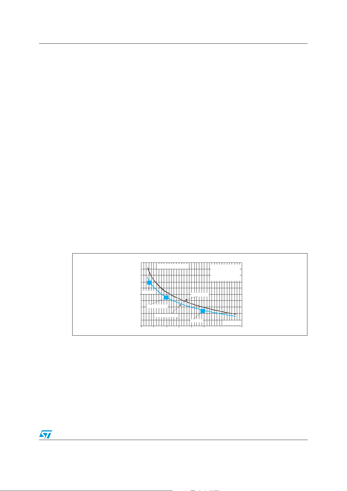
1.2 VF, Qrr trade-off for the three families
The three families are: STTHxxR06 (R stands for rapid with low Qrr), STTHxx06 (medium VF
and Q
Figure 1 shows where a trade-off occurs in three operational areas. A technology using gold
doping is also shown.
Figure 1. V
), and STTHxxL06 (Low forward voltage).
rr
- Qrr trade-off for an 8 A diode
F
V (V)
F
1.7
Typical values
) doping. Pt doping is required
t
IF= 8 A
VR= 400 V
dIF/dt = 200 A/µs
Tj= 125 °C
R Family
1.2
Medium Family
Platinum doping
0.7
0 200 400 600 800 1000 1200 1400 1600
Gold doping
L Family
Qrr(nC)
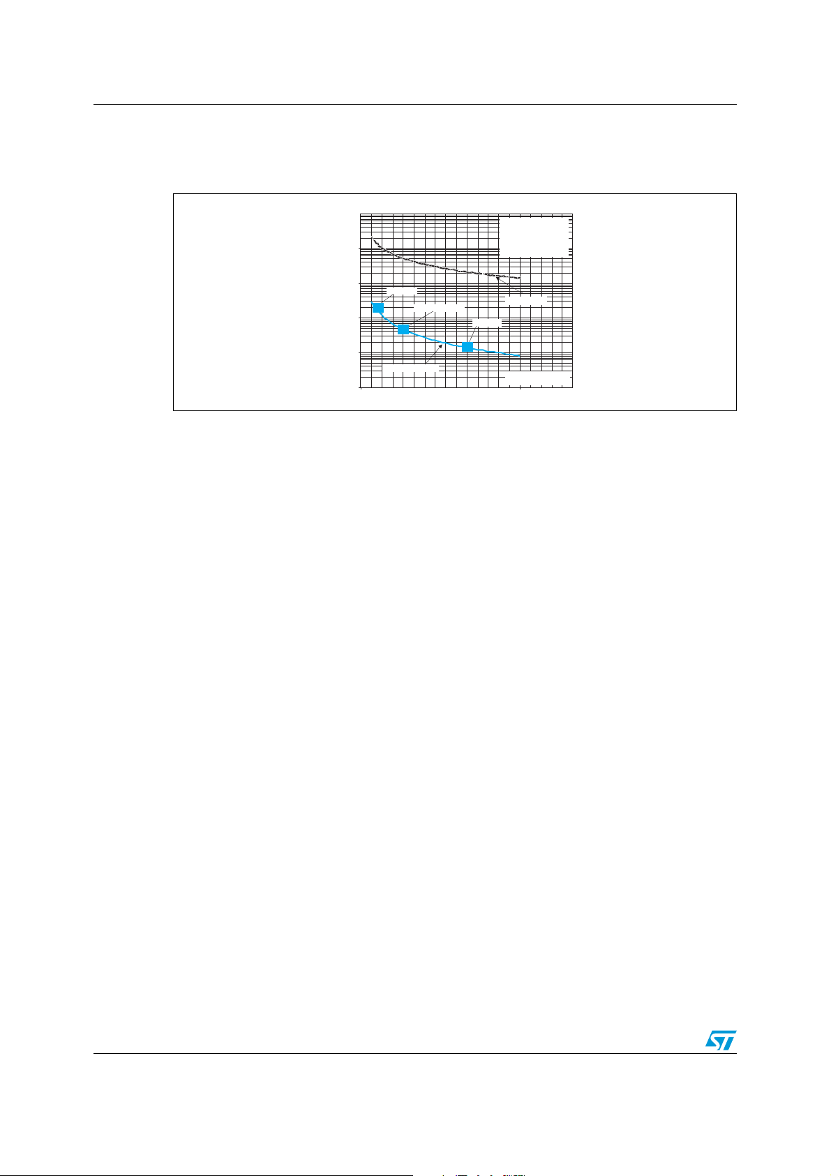
1.3 Platinum doping and low leakage current
Figure 2 shows the trade-off between leakage current IR and Q
areas. The faster the diode, the higher the I
doping. For the same Q
, IR is approximately 100 times lower with platinum doping. The
rr
corresponding “R” family with gold doping would have a high maximum leakage current
(18 mA at 125 °C and 400 V). As shown later in this Application note, with such a leakage
current thermal instability can be reached for operating junction temperatures higher than
125 °C in a conventional application.
Doc ID 018581 Rev 1 3/18
is. This rule is true for both gold and platinum
R
in several operational
rr
General information AN3358
1
10
100
1000
10000
100000
0 500 1000 1500 2000
It will also be shown that IR is also a critical parameter for diodes in axial and SMD
packages.
Figure 2. I
- Qrr trade-off in several operational areas for an 8 A diode
R
I (µA)
Rmax
IF= 8 A
VR= 400 V
dIF/dt = 200 A/µs
Tj= 125 °C
R Family
Medium Family
Platinum doping
L Family
Gold doping
Q
rr typ
(nC)
4/18 Doc ID 018581 Rev 1
AN3358 Main applications of 600 V ultrafast diodes
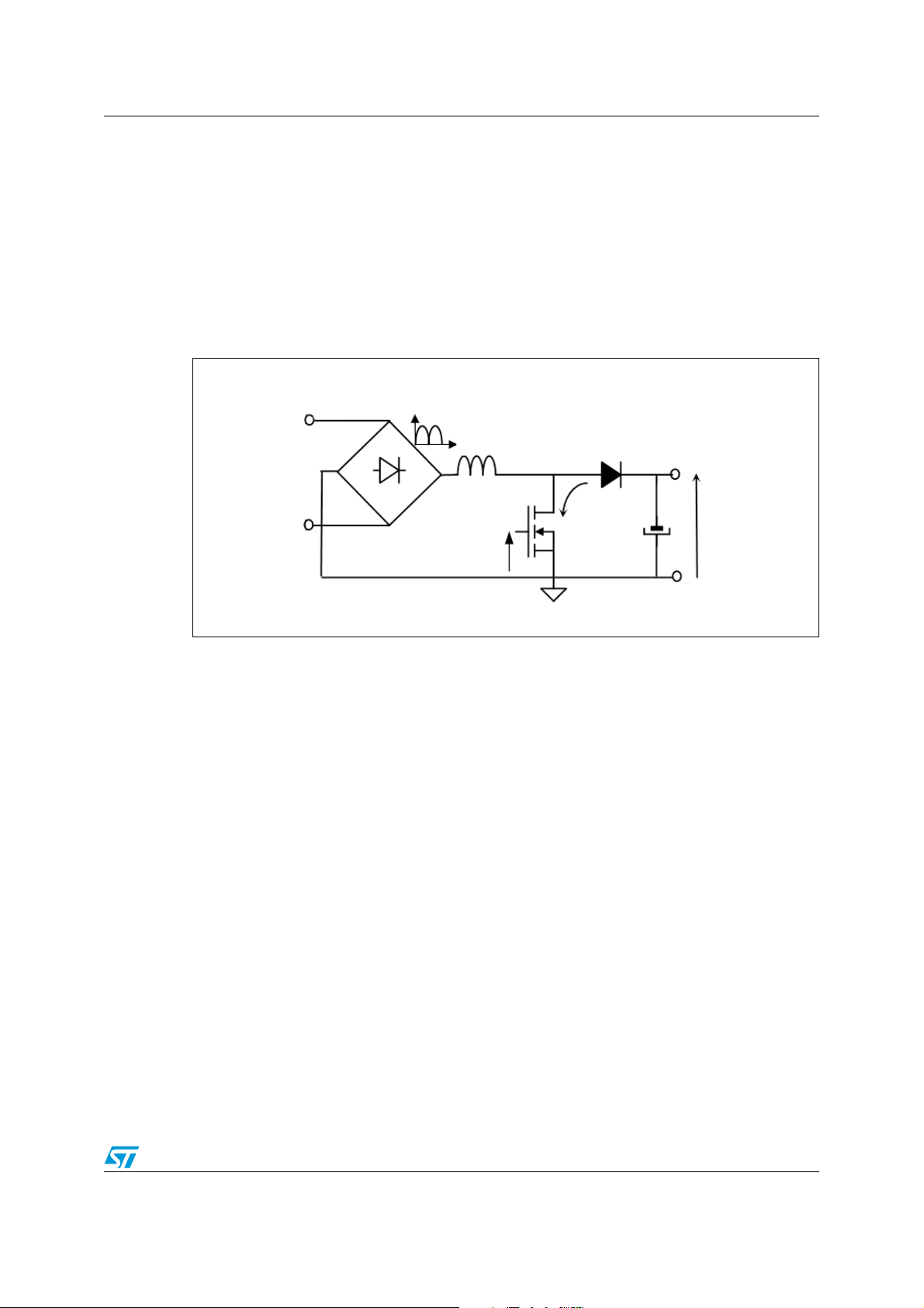
2 Main applications of 600 V ultrafast diodes
This section discusses the trade-offs in a common application. Boost power factor corrector
(PFC) will be widely covered since it is a major application. A typical PFC circuit is shown in
Figure 3.
2.1 Power factor corrector applications
Figure 3. Boost power factor corrector circuit
V
mains
L
V
gate
D
boost
I
RM
2.1.1 Boost diode in PFC working in continuous mode
Hard switching conditions
PFC applications are mainly designed in continuous mode when the power is greater than
200 W.
In such an application, it is well known that the greatest losses due to the diode are the
switching losses in the transistor (P
of the boost diode flows into the MOSFET (Figure 3). Consequently, the best choice in most
cases is the “R” family.
Switching losses due to I
temperature T
and the mains voltage V
j
depend mainly on two parameters: the operating junction
RM
Figure 4 and Figure 5 show that the switching losses for STTH8R06 quickly increase when
T
increases and when V
j
decreases. These curves are drawn with a software tool
mains
realized by these authors.
) when it turns on. The reverse recovery current (IRM)
ontr
.
mains
V
out
If the PFC only works on 240 V mains, with a low operating junction temperature, switching
losses will be less critical and the best trade-off could be the intermediate trade-off:
STTHxx06.
However, most PFCs are designed to work in a wide mains voltage range (85 V-264 V) with
an operating junction temperature (in the worst case) close to 100 °C. The “R” family will be
the family usually recommended.
Doc ID 018581 Rev 1 5/18
Main applications of 600 V ultrafast diodes AN3358
Figure 4. Switching losses versus Tj at turn off of the diode
P diode + P due to the diode (W)
off ontr
14
12
10
STTH8R06D
8
6
4
2
0
0 25 50 75 100 125 150 175
Figure 5. Switching losses versus V
P diode + P due to the diode (W)
off ontr
12
10
8
6
4
2
0
0 50 100 150 200 250 300
V = 90 V
mains
dI/dt = 400 A/µs
L = 0.5 mH
F = 100 kHz
sw
V = 400 V
OUT
P = 400 W
OUT
at turn off of the diode
mains
STTH8R06D
T = 100 °C
dI/dt = 400 A/µs
L = 0.5 mH
F = 100 kHz
sw
V = 400 V
OUT
P = 400 W
OUT
T (°C)
j
j
V (V)
mains
6/18 Doc ID 018581 Rev 1

AN3358 Main applications of 600 V ultrafast diodes
T
before thermal runaway
jmax
The maximum junction temperature T
before thermal runaway can be calculated using
jmax
Equation 1, Equation 2 then Equation 3.
Equation 1
2 V
δ = 1 -
mains peak
π V
OUT
Equation 2
I(V ,T )
R OUT jmax
=
V · c R
1
δ·
OUT th(j-a)
Equation 3
T = 125 +
jmax
1
c
· log
I(V T )
R OUT, jmax
e
(
I (V 125 °C)
Rmax OUT,
(
Where:
● δ is the average duty cycle of the blocking time of the diode given by Equation 3.
● V
● c is a constant with units of °C
is the output voltage.
OUT
-1
. Each diode has its own “c” coefficient depending on
the technology of the diode and the reverse voltage V
applied. It can be determined
R
from Equation 3 for two values of leakage curr ent correspond ing to applicatio n reverse
● R
voltage V
th(j-a)
, for example: IR(V
out
,100 °C) and IR(V
out
,125 °C).
out
is the thermal resistance between junction and ambient (heatsink + diode).
With the following conditions:
V
= 400 V, c ≈ 0.055 °C
OUT
V
= 85 V, δ = 0.8, R
mains
Figure 2 gives I
Rmax(400 V, 125 °C)
-1
(for the “R” family)
= 10 °C/W
th(j-a)
= 215 µA for an 8 A “R” family diode and 17 mA for the
equivalent diode in gold doping.
Equation 2 and Equation 3 give T
= 184 °C for Turbo2 and 104 °C for the equivalent
jmax
diode in gold doping.
Soft switching condition
Designers can use a number of techniques to turn on the MOSFET in soft switching
conditions and reduce the switching losses due to I
Figure 6 and Figure 7 show two solutions, widely used with the associated waveforms
during switching time. In the non-dissipative circuit Figure 6, the smaller transistor T2 turns
on before the main one T1. The dl/dt when D
boost
and T1 turns on at zero current. Consequently, the switching-on losses will be close to zero.
With this circuit, the reverse recovery current of the boost diode is less critical. The best
choice, following the application conditions (switching frequency, L
intermediate” or the “L” trade-off.
Doc ID 018581 Rev 1 7/18
.
RM
turns off is controlled by Lr (dl/dt = V
…) will be “the
r
out/Lr
),

Main applications of 600 V ultrafast diodes AN3358
Figure 6. Non-dissipative soft switching solution
V
mains
D
boost
L
r
D
r
T
1on
V
out
T1, T2
L
C
T
1
r
T
2
I
0+IRM
IRM+I
I
DBoost
V
res
T
I
0
I
Lr
2on
V
⎛
⎞
OUT
⎜
⎟
L
⎝
⎠
r
I
RM
I0+IRM+I
I
Dr
Cr
I
T1
t
t
res
t
t
t
t
8/18 Doc ID 018581 Rev 1

AN3358 Main applications of 600 V ultrafast diodes
The topology shown in Figure 7 is more simple but more dissipative than that in Figure 6.
The waveforms in Figure 7 show the MOSFET turning on at zero current, thus reducing the
switching losses. When the diode turns off, the L
inductor is charged with the reverse
r
recovery current of the boost diode. This energy will be dissipated in the resistor.
The higher I
is the higher the losses in the resistor are. In this application IRM is more
RM
critical than in the previous one. The best choice for the boost diode trade-off will be “R” or
medium family depending on the application conditions.
Figure 7. Dissipative soft switching solution
D
V
mains
L
DBoost
V
DS
r
L
r
V
RC
V
OUT
T
450 V
250 V
I
T
V
DS
20 A
10 A
180.8
180.8
0A
-10 A
20 A
10 A
0A
-8 A
0V
-250 V
60 V
40 V
20 V
0V
180.0
180.0
I
DBoost
180.4
180.4
180.5
180.5
180.6
180.6
t (µs)
180.7
t (µs)
180.7
V
180.1
RC
180.1
I
RM
180.2
I
Dr
180.2
180.3
I
DBoost
I
Lr
180.3
Q
rr
Another very interesting alternative soft switching solution is described in the application
note AN3276, “ST solution for efficiency improvement in PFC applications, back current
circuit (BC2)”. AN3276 presents a patented soft switching circuit from STMicroelectronics
offering performance similar to that of SiC Schottky diodes.
Doc ID 018581 Rev 1 9/18

Main applications of 600 V ultrafast diodes AN3358
2.1.2 Boost diode in PFC working in transition mode
The transition mode (TM) is widely used for low power PFC (<200 W). The particularity of
this control mode working between continuous and transition mode is a simple control and a
few external components. This control mode results in variable frequency operation and a
constant on time of the MOSFET.
Consequently, the current flowing through the Boost inductor is triangular (Figure 8). It
increases through the MOSFET following the slope defined by V
through the diode following a low dl/dt given in Equation 4.
Equation 4
mains
V
-
OUT
L
dI
V
=
dt
In this case dI/dt may have a value up to 0, the necessary condition for the next cycle.
Figure 8. Inductor current waveform and MOSFET timing
P
I
P
K
=2 2x
OUT
V
mains
Average
input current
/L, and decreases
mains
Inductor
current
V
mains
L
V-V
mains out
L
T =
2 · F
1
mains
N
=
F
SW
On
MOSFET
Off
t fixed
on
T variable
SW
The ZCD circuit (zero current detection) turns on the MOSFET at zero current, avoiding high
switching losses in the MOSFET due to the recovery charge of the diode.
Unlike the continuous mode, the Q
of the diode it is not the key parameter any more. In the
rr
transition mode, the main losses of the diode are due to the forward voltage. It is then
possible to optimize the V
parameter to the detriment of Qrr, due to the low dl/dt
F
of the
off
diode (<1 A/µs) fixed by the inductor.
10/18 Doc ID 018581 Rev 1

AN3358 Main applications of 600 V ultrafast diodes
Nevertheless, an accurate study at switch-off of the diode shows that the Qrr parameter
cannot be indefinitely relaxed. Figure 9 highlights this phase when the current of the diode
reaches 0, and shows that this time is composed of 3 phases:
● Phase 1 [t0,t1]: The diode is open. There is a resonant circuit between the equivalent
capacitance (C
condition the I
● Phase 2 [t1,t2]: V
conduction and the current linearly increases through the V
● Phase 3 at t2: The ZCD circuit turns the MOSFET on and the current continues to
linearly rise through the R
MOS + Cj diode) and the boost inductance, which has as its initial
ds
of the diode.
RM
reaches 0 and the body diode of the MOSFET enters in
DS
DS(on)
.
of the body diode.
F
Figure 9. Switch-off comparison between STTH1L06 and a slower diode
t
t
t
2
1
0
I
RM
I
Diode
VdsV
ds
Slower diode
V
grille
I
Mos
STTH1L06
It can be observed that the dead time (t0,t2) increases with the I
of the diode. This time a
RM
negative current flows through the power MOSFET and is the source of additional losses.
This duration depends on the slope (versus V
, L) and also on the IRM of the diode (the
mains
initial condition of phase 1). During this time there is no power transferred to the load. In this
way, with a very slow diode, the sum of the losses due to high I
compared to these of the conduction losses. Therefore, there is a limit for Q
cannot be negligible
RM
. This limit
rr
appears for the full range PFC at 110 V. In this condition the current in the power MOSFET
takes more time to reach 0 (maximum dead time).
The maximum Q
of the “L” family has been optimized taking these considerations into
rr
account.
According to the application conditions (P
out
, V
mains
, dI/dt
, Fsw, Tj), the medium trade-off
max
could be also considered. The optimum choice between low forward voltage trade-off
(STTHxxL06) and the medium trade-off (STTHxx06) could be determined by efficiency
measurement.
In transition mode a diode with a small current rating is used. It is generally a small package
(axial or SMD packages) with high thermal resistances. Consequently, the junction
Doc ID 018581 Rev 1 11/18

Main applications of 600 V ultrafast diodes AN3358
temperature of the diode, which is mainly fixed by the conduction losses, can be high.
Equation 2 in Section 2.1 shows that the thermal resistance is a critical parameter for the
thermal runaway limit. Tabl e 1 compares the thermal runaway limit between Turbo2 and a
gold-doped diode working in a transition mode PFC in the following conditions:
R
= 75 °C/W, c ≈ 0.072 °C
th(j-a)
Table 1. T
125 °C, 400 V 15 µA 1.5 mA
I
Rmax
T
before thermal runaway
jmax
comparison between Turbo2 and gold doping diode
jmax
limit is reached.
-1
, V
= 400 V, V
OUT
= 85 V, δ = 0.808
mains
STTH3L06 Gold Doping
176 °C 112 °C
This comparison shows that gold-doped diodes are limited in high temperature. There is no
thermal runaway risk when Turbo2 uses platinum doping. For all these reasons, in most
cases, the “L” family is recommended for the PFC application working in transition mode.
2.1.3 Boost diode working in fixed-off-time (FOT) PFC
In this third PFC operating mode, instead of maintaining the on-time fixed, such as TM PFC,
the T
drained from the source according to the load.
is kept constant and the Ton is free to be changed in order to modulate the power
off
This modulation method, is described in the Application note AN1792, “Design of fixed-offtime controller PFC pre-regulators with L6562”.
As shown in Figure 10 in FOT mode, the PFC works in DCM and CCM modes along the line
semi period.
Figure 10. Inductor, switch and diode currents in a CCM FOT-controlled PFC stage
DCM
Switch current
Switch
CCM
ILpk
θt
OFF OFF
Inductor current
peak envelope
DCM
Low frequency
inductor current
Diode current
ON
OFF
π−θt
12/18 Doc ID 018581 Rev 1

AN3358 Main applications of 600 V ultrafast diodes
In this operating mode, according to the application conditions the optimal diode will be the
medium trade-off (V
) or the rapid trade-off (“R” family). The designer should make
F/QRR
some measurements of efficiency to confirm the good trade-off diode in its application.
2.2 Other applications
There are numerous other electronic functions, where 600 V ultrafast diodes are used. For
example, rectification, demagnetization, snubber, bootstrapping, clamping, or East-West
correction in a horizontal deflection circuit for TV or monitor (Figure 11).
Figure 11. Traditional applications of 600 V ultrafast diodes
Clamping diode
Snubber diode
Demagnetization diode
Bootstrap diode
Modulator diode in horizontal deflection circuit
Doc ID 018581 Rev 1 13/18

Main applications of 600 V ultrafast diodes AN3358
It is not possible in this document to analyze each function in detail. We will focus on the
clamping function used in flyback converters. The function of the clamping circuit is to
protect the MOSFET against the overvoltage due to the energy in the leakage inductance of
the transformer. The associated waveforms are represented in Figure 12.
Figure 12. 600 V ultrafast diode waveforms in clamping function
V
mains
V
Lf
or
V
V
IN
C
V
DCL
m
D
CL
V
D
R
V
OUT
DS
V
DS
I
CL
D
I
CL
I
DR
V
DCL
D
Qrr
Breakdown voltage of the MOS transistor
VDS=VIN+VC+V
V
Lf
I
DR
VIN+(V
V
FP
/m)
OUT
IN
V
CEsat
V
FP
V
Rmax=VIN+VC
+S
pike
14/18 Doc ID 018581 Rev 1

AN3358 Main applications of 600 V ultrafast diodes
When the MOSFET turns off, the inductive circuit opens and an overvoltage VLf appears in
addition to the voltage across the primary inductor V
turns on the clamping diode. Thus, the drain voltage is equal to V
V
is the peak forward voltage across the 600 V diode. VC is a DC voltage realized either
FP
/m. The effect of this overvoltage
OUT
= VIN + VC +VFP.
DS
by an RC circuit in parallel or by a clamping diode such as a Transil™.
The first key parameter of the diode is V
of the MOSFET. If V
is too high the designer may be obliged to choose a higher voltage
FP
FP. VDS
has to be lower than the breakdown voltage
MOSFET (for example 800 V instead of 600 V).
To avoid thermal runaway problems a low value of leakage current is necessary as the diode
is normally a 1 A device in an SMD or axial package. A low I
will also contribute to the
R
reduction of consumption in stand-by mode. The forward voltage is not a critical parameter
because the diode conducts about ten nanoseconds every switching period.
When the clamping voltage is made with a Transil, it is generally better to use an ultrafast
type diode. When an RC solution is used, the capacitance is discharged through the reverse
recovery current of the diode, thus reducing the losses in the resistor.
The Turbo2 technology, which allows low leakage current and low peak forward voltage, is
well suited for this application. The best trade-off with a Transil, will be the “R” or the medium
family. With an RC solution the choice will generally be between the “L” and the “medium”
families.
TM: Transil is a trademark of STMicroelectronics
Doc ID 018581 Rev 1 15/18

Conclusion AN3358
3 Conclusion
This Application note presents the main applications of the 600 V ultrafast diodes. These
applications are numerous, each requiring a slightly different trade-off among the diode
parameters. In order to propose an optimized solution for each one, three trade-offs are
proposed by STMicroelectronics. There are some general rules to define the right trade-off.
For example, the “R” family for PFC working in continuous mode and hard switching
condition and the “L” family for PFC working in transition mode. However, there are also
applications for which a deeper study will be necessary.
An important benefit of the platinum doping implemented in the Turbo2 technology resides
in the use of the diodes at high junction temperature without thermal runaway risk in normal
prescribed condition of use (<175 °C).
16/18 Doc ID 018581 Rev 1

AN3358 References
4 References
[1] ST Application note AN628, “Designing a high power factor switching preregulator with
the l4981 continuous mode”
[2] PCIM, Nuremburg, 2000 “New solution to optimize diode recovery in PFC boost
converter”, B. Rivet.
[3] ST Application note AN667, “Designing a high power factor switching preregulator with
the l6560 transition mode”
[4] ST Application note AN966, “Enhanced transition mode power factor corrector”
[5] ST Application note AN1792, “Design of fixed-off-time controller PFC preregulator with
the L6562”
[6] ST Application note AN3276, “ST solution for efficiency improvement in PFC
applications, back current circuit (BC
5 Revision history
Table 2. Document revision history
Date Revision Changes
14- Sep-2011 1 First issue
2
)”
Doc ID 018581 Rev 1 17/18

AN3358
Please Read Carefully:
Information in this document is provided solely in connection with ST products. STMicroelectronics NV and its subsidiaries (“ST”) reserve the
right to make changes, corrections, modifications or improvements, to this document, and the products and services described herein at any
time, without notice.
All ST products are sold pursuant to ST’s terms and conditions of sale.
Purchasers are solely responsible for the choice, selection and use of the ST products and services described herein, and ST assumes no
liability whatsoever relating to the choice, selection or use of the ST products and services described herein.
No license, express or implied, by estoppel or otherwise, to any intellectual property rights is granted under this document. If any part of this
document refers to any third party products or services it shall not be deemed a license grant by ST for the use of such third party products
or services, or any intellectual property contained therein or considered as a warranty covering the use in any manner whatsoever of such
third party products or services or any intellectual property contained therein.
UNLESS OTHERWISE SET FORTH IN ST’S TERMS AND CONDITIONS OF SALE ST DISCLAIMS ANY EXPRESS OR IMPLIED
WARRANTY WITH RESPECT TO THE USE AND/OR SALE OF ST PRODUCTS INCLUDING WITHOUT LIMITATION IMPLIED
WARRANTIES OF MERCHANTABILITY, FITNESS FOR A PARTICULAR PURPOSE (AND THEIR EQUIVALENTS UNDER THE LAWS
OF ANY JURISDICTION), OR INFRINGEMENT OF ANY PATENT, COPYRIGHT OR OTHER INTELLECTUAL PROPERTY RIGHT.
UNLESS EXPRESSLY APPROVED IN WRITING BY TWO AUTHORIZED ST REPRESENTATIVES, ST PRODUCTS ARE NOT
RECOMMENDED, AUTHORIZED OR WARRANTED FOR USE IN MILITARY, AIR CRAFT, SPACE, LIFE SAVING, OR LIFE SUSTAINING
APPLICATIONS, NOR IN PRODUCTS OR SYSTEMS WHERE FAILURE OR MALFUNCTION MAY RESULT IN PERSONAL INJURY,
DEATH, OR SEVERE PROPERTY OR ENVIRONMENTAL DAMAGE. ST PRODUCTS WHICH ARE NOT SPECIFIED AS "AUTOMOTIVE
GRADE" MAY ONLY BE USED IN AUTOMOTIVE APPLICATIONS AT USER’S OWN RISK.
Resale of ST products with provisions different from the statements and/or technical features set forth in this document shall immediately void
any warranty granted by ST for the ST product or service described herein and shall not create or extend in any manner whatsoever, any
liability of ST.
ST and the ST logo are trademarks or registered trademarks of ST in various countries.
Information in this document supersedes and replaces all information previously supplied.
The ST logo is a registered trademark of STMicroelectronics. All other names are the property of their respective owners.
© 2011 STMicroelectronics - All rights reserved
STMicroelectronics group of companies
Australia - Belgium - Brazil - Canada - China - Czech Republic - Finland - France - Germany - Hong Kong - India - Israel - Italy - Japan -
Malaysia - Malta - Morocco - Philippines - Singapore - Spain - Sweden - Switzerland - United Kingdom - United States of America
www.st.com
18/18 Doc ID 018581 Rev 1
 Loading...