

Page 1

AN3316
Application note
SPC560B power and mode management
Introduction
This application note is intended for system designers who require a hardware
implementation overview of the low-power modes of the SPC560B product family. It shows
how to use the SPC560B product family in these modes and describes how to take power
consumption measurements. Example firmware is provided with this application note for
implementing and measuring the consumption and wake-up time of the different SPC560B
family’s functioning modes.
November 2010 Doc ID 18232 Rev 1 1/42
www.st.com
Page 2

Contents AN3316
Contents
1 Power consumption factors . . . . . . . . . . . . . . . . . . . . . . . . . . . . . . . . . . . 5
1.1 Overview . . . . . . . . . . . . . . . . . . . . . . . . . . . . . . . . . . . . . . . . . . . . . . . . . . 5
1.2 Dynamic power reduction . . . . . . . . . . . . . . . . . . . . . . . . . . . . . . . . . . . . . . 5
1.3 Static power reduction . . . . . . . . . . . . . . . . . . . . . . . . . . . . . . . . . . . . . . . . 7
2 Device modes . . . . . . . . . . . . . . . . . . . . . . . . . . . . . . . . . . . . . . . . . . . . . . 9
2.1 Modes overview . . . . . . . . . . . . . . . . . . . . . . . . . . . . . . . . . . . . . . . . . . . . . 9
2.2 Modes description . . . . . . . . . . . . . . . . . . . . . . . . . . . . . . . . . . . . . . . . . . 10
2.2.1 System modes . . . . . . . . . . . . . . . . . . . . . . . . . . . . . . . . . . . . . . . . . . . . 10
2.2.2 Running modes . . . . . . . . . . . . . . . . . . . . . . . . . . . . . . . . . . . . . . . . . . . 11
2.2.3 Low Power modes . . . . . . . . . . . . . . . . . . . . . . . . . . . . . . . . . . . . . . . . . 11
2.3 Key advantages of Mode Entry . . . . . . . . . . . . . . . . . . . . . . . . . . . . . . . . 12
2.3.1 Transition control . . . . . . . . . . . . . . . . . . . . . . . . . . . . . . . . . . . . . . . . . . 12
2.3.2 Modules/peripherals configuration . . . . . . . . . . . . . . . . . . . . . . . . . . . . . 12
2.3.3 HW failure and error modes management . . . . . . . . . . . . . . . . . . . . . . . 16
2.4 Application cases . . . . . . . . . . . . . . . . . . . . . . . . . . . . . . . . . . . . . . . . . . . 17
2.4.1 Power-on reset phase (RESET → DRUN) . . . . . . . . . . . . . . . . . . . . . . . 18
2.4.2 Application scenarios . . . . . . . . . . . . . . . . . . . . . . . . . . . . . . . . . . . . . . 18
3 Consumption tables . . . . . . . . . . . . . . . . . . . . . . . . . . . . . . . . . . . . . . . . 34
3.1 Running mode . . . . . . . . . . . . . . . . . . . . . . . . . . . . . . . . . . . . . . . . . . . . . 34
3.2 Low Power modes . . . . . . . . . . . . . . . . . . . . . . . . . . . . . . . . . . . . . . . . . . 35
3.2.1 HALT consumption . . . . . . . . . . . . . . . . . . . . . . . . . . . . . . . . . . . . . . . . . 35
3.2.2 STOP consumption . . . . . . . . . . . . . . . . . . . . . . . . . . . . . . . . . . . . . . . . 36
3.2.3 STANDBY consumption . . . . . . . . . . . . . . . . . . . . . . . . . . . . . . . . . . . . . 38
3.3 Peripherals . . . . . . . . . . . . . . . . . . . . . . . . . . . . . . . . . . . . . . . . . . . . . . . . 38
3.4 Consumption example . . . . . . . . . . . . . . . . . . . . . . . . . . . . . . . . . . . . . . . 39
4 Revision history . . . . . . . . . . . . . . . . . . . . . . . . . . . . . . . . . . . . . . . . . . . 41
2/42 Doc ID 18232 Rev 1
Page 3

AN3316 List of tables
List of tables
Table 1. Module configuration . . . . . . . . . . . . . . . . . . . . . . . . . . . . . . . . . . . . . . . . . . . . . . . . . . . . . 13
Table 2. Clock configuration . . . . . . . . . . . . . . . . . . . . . . . . . . . . . . . . . . . . . . . . . . . . . . . . . . . . . . . 14
Table 3. Loop divide ratio . . . . . . . . . . . . . . . . . . . . . . . . . . . . . . . . . . . . . . . . . . . . . . . . . . . . . . . . . 21
Table 4. Input divide ratio . . . . . . . . . . . . . . . . . . . . . . . . . . . . . . . . . . . . . . . . . . . . . . . . . . . . . . . . . 21
Table 5. Output divide ratio. . . . . . . . . . . . . . . . . . . . . . . . . . . . . . . . . . . . . . . . . . . . . . . . . . . . . . . . 22
Table 6. SPC560B54/6x peripheral clock sources . . . . . . . . . . . . . . . . . . . . . . . . . . . . . . . . . . . . . . 22
Table 7. Peripherals clock source. . . . . . . . . . . . . . . . . . . . . . . . . . . . . . . . . . . . . . . . . . . . . . . . . . . 25
Table 8. RUN0 mode consumption table . . . . . . . . . . . . . . . . . . . . . . . . . . . . . . . . . . . . . . . . . . . . . 34
Table 9. RUN0 mode consumption example . . . . . . . . . . . . . . . . . . . . . . . . . . . . . . . . . . . . . . . . . . 35
Table 10. HALT mode consumption table . . . . . . . . . . . . . . . . . . . . . . . . . . . . . . . . . . . . . . . . . . . . . 35
Table 11. HALT mode consumption example . . . . . . . . . . . . . . . . . . . . . . . . . . . . . . . . . . . . . . . . . . . 36
Table 12. STOP mode consumption table . . . . . . . . . . . . . . . . . . . . . . . . . . . . . . . . . . . . . . . . . . . . . 37
Table 13. STOP mode consumption example . . . . . . . . . . . . . . . . . . . . . . . . . . . . . . . . . . . . . . . . . . 37
Table 14. STANDBY mode consumption table . . . . . . . . . . . . . . . . . . . . . . . . . . . . . . . . . . . . . . . . . . 38
Table 15. Peripherals consumption table . . . . . . . . . . . . . . . . . . . . . . . . . . . . . . . . . . . . . . . . . . . . . . 39
Table 16. Peripherals consumption example . . . . . . . . . . . . . . . . . . . . . . . . . . . . . . . . . . . . . . . . . . . 40
Table 17. Document revision history . . . . . . . . . . . . . . . . . . . . . . . . . . . . . . . . . . . . . . . . . . . . . . . . . 41
Doc ID 18232 Rev 1 3/42
Page 4

List of figures AN3316
List of figures
Figure 1. Peripheral clock . . . . . . . . . . . . . . . . . . . . . . . . . . . . . . . . . . . . . . . . . . . . . . . . . . . . . . . . . . 5
Figure 2. Global clock tree architecture . . . . . . . . . . . . . . . . . . . . . . . . . . . . . . . . . . . . . . . . . . . . . . . . 6
Figure 3. SPC560B54/6x power domain structure. . . . . . . . . . . . . . . . . . . . . . . . . . . . . . . . . . . . . . . . 7
Figure 4. MC_ME mode diagram . . . . . . . . . . . . . . . . . . . . . . . . . . . . . . . . . . . . . . . . . . . . . . . . . . . . 10
Figure 5. Power Domain 0 architecture . . . . . . . . . . . . . . . . . . . . . . . . . . . . . . . . . . . . . . . . . . . . . . . 12
Figure 6. Mode transition example. . . . . . . . . . . . . . . . . . . . . . . . . . . . . . . . . . . . . . . . . . . . . . . . . . . 14
Figure 7. Peripheral configuration example . . . . . . . . . . . . . . . . . . . . . . . . . . . . . . . . . . . . . . . . . . . . 15
Figure 8. HW failure example . . . . . . . . . . . . . . . . . . . . . . . . . . . . . . . . . . . . . . . . . . . . . . . . . . . . . . 17
Figure 9. Transition (HW start-up) RESET → DRUN (execution from CFlash) . . . . . . . . . . . . . . . . . 18
Figure 10. Node configuration . . . . . . . . . . . . . . . . . . . . . . . . . . . . . . . . . . . . . . . . . . . . . . . . . . . . . . . 19
Figure 11. Transition step . . . . . . . . . . . . . . . . . . . . . . . . . . . . . . . . . . . . . . . . . . . . . . . . . . . . . . . . . . 20
Figure 12. Scenario 2 - finite state machine . . . . . . . . . . . . . . . . . . . . . . . . . . . . . . . . . . . . . . . . . . . . 23
Figure 13. Scenario 2 - flow chart . . . . . . . . . . . . . . . . . . . . . . . . . . . . . . . . . . . . . . . . . . . . . . . . . . . . 24
Figure 14. Scenario 3 - finite state machine . . . . . . . . . . . . . . . . . . . . . . . . . . . . . . . . . . . . . . . . . . . . 26
Figure 15. Scenario 3 - flow chart . . . . . . . . . . . . . . . . . . . . . . . . . . . . . . . . . . . . . . . . . . . . . . . . . . . . 27
Figure 16. Scenario 4 - finite state machine . . . . . . . . . . . . . . . . . . . . . . . . . . . . . . . . . . . . . . . . . . . . 29
Figure 17. Scenario 4 - flow chart . . . . . . . . . . . . . . . . . . . . . . . . . . . . . . . . . . . . . . . . . . . . . . . . . . . . 30
Figure 18. Power domain . . . . . . . . . . . . . . . . . . . . . . . . . . . . . . . . . . . . . . . . . . . . . . . . . . . . . . . . . . . 32
Figure 19. STANDBY transition . . . . . . . . . . . . . . . . . . . . . . . . . . . . . . . . . . . . . . . . . . . . . . . . . . . . . . 33
4/42 Doc ID 18232 Rev 1
Page 5

AN3316 Power consumption factors
1 Power consumption factors
1.1 Overview
As SPC560B is a CMOS digital logic device, total power consumption is:
P
TOTAL
= P
DYNAM IC
+ P
STATIC
Where:
● P
DYNAMIC
is the dynamic power contribution that depends on the supply voltage and
the clock frequency through following formula:
P
DYNAM IC
= α · CV2f
with:
– C is the CMOS load capacitance
– V is the 5 V supply voltage
– f is the clock frequency
● P
is the static power contribution that depends mainly on the transistor
STATIC
polarization and leakage as in the following formula:
P
STATIC=ISTATIC
V
So to minimize total power consumption, it is needed to minimize each dynamic/static
contribution which strongly depends on clock frequency and the clock structure
implemented.
1.2 Dynamic power reduction
SPC560B adopts a very smart clock tree architecture in which all the clock sources are not
directly routed to peripherals. In fact, a peripheral bus block is located in the middle to divide
or disable all the clocks connected to the peripherals to save power consumption.
Figure 1. Peripheral clock
/
System clk
div 1 to 15
So, looking at the global clock tree architecture:
Doc ID 18232 Rev 1 5/42
Peripheral set x
Page 6

Power consumption factors AN3316
Figure 2. Global clock tree architecture
OSC
&
16MHz
IRC
16MHz
OSC
32KHz
IRC
128KHz
div 1 to 32
div 1 to 32
FMPLL
irc_fast
osca_clk
oscb_clk
irc_slow
div 1 to 32
div 1 to 32
osca_clk_div
irc_fast_div
CMU
osca_clk
osca_fast
fmplla_clk
System
Clock
Selector
(ME)
irc_slow_div
CLKOUT
Selector
RESET
SAFE
INT
system_clk
div 1 to 15
div 1 to 15
div 1 to 15
irc_fast_div
oscb_clk_div
div 1/2/4/8
Core
Platform
Peripheral Set 1
Peripheral Set 2
Peripheral Set 3
API / RTC
SWT
(Watchdog)
CLOCK OUT
It is possible to decrease power consumption through following features:
● Reduced number of directly clocked lines (see red circle on Figure 2)
● Reduced local clock rates through peripheral bus division (see blue circle on Figure 2)
ModeEntry Module is also structured to help reduce dynamic power consumption as:
● Allows to clock-gate each peripheral independently. So, power saving can be achieved
by clock-gating peripherals not used in the application.
● Allows to switch-off the CPU which is the most power-hungry part in the device. For
example, while waiting for an ADC conversion to complete.
6/42 Doc ID 18232 Rev 1
Page 7
AN3316 Power consumption factors
1.3 Static power reduction
The two main system/market constraints that influenced SPC560B definition:
● Request for more performance/integration and cost reductions leading to the usage of
more and more advanced and small technologies
● Carmakers’ constraints to maintain functions even when the car is switched off with a
max consumption of 100µA to 1mA for the overall ECU and depending on its type,
BCM, door module etc.
In order to match these two constraints, ST developed the SPC560B with following features:
● Adopting 90nm technology to meet integration/costs but with using a low leakage
technology (Leakage minimization)
● Subdividing device into following different PD0, PD1, PD2, PD3 power domains to meet
LP function/consumption (Power Segmentation)
These domains are individually disconnected from Power and so eliminates the leakage
from the areas they are turned off.
Figure 3. SPC560B54/6x power domain structure
Vreg
&
power
gating
LV
LV
HV
LV
HV
LV
64K
RAM
24K
RAM
API/
RTC
Wake-up
Logic
PD3
RAM Domain 2
PD2
RAM Domain 1
Platform XOSCZO core
Peripheral
Set One
Reset &
Wake-up
vector
Peripheral
Set Two
128KHz
IRC
JTAG
16 Mhz
IRC
Notes:
LV = Low Voltage(1.2V on SPC560B)
HV = High Voltage(3.3V on SPC560B)
PD = Power Domain
RD = RAM Power Domain
PCU = Power Control Unit
RGM = Reset Generation Module
CGM = Clock Generation Module
CGL = Clock Gating Logic
ME = mode Entry unit
CGM CGL ME
PLL
Part of
Magic Carpet
PCU RGM
8K
RAM
32KHz
XTAL
PD1
Micro
domain
PD0
Always 0
domain
CAN
Sampler
Doc ID 18232 Rev 1 7/42
Page 8

Power consumption factors AN3316
Notice that Power Domains shown on Figure 3 are related to SPC560B54/6x, where:
● Power Domain PD0:
–always on
– wakeup peripheries like the CAN sampler, the RTC, API, etc.
– minimum RAM segment (8 K)
● Power Domain PD1:
– contains all cores and the majority of peripherals
– can be turned off in STOP or STANDBY modes
– must be turned on in RUN modes (although there is a clock gating option for all
peripherals and also a WAIT instruction for the cores to reduce power)
● Power Domain PD2:
– additional RAM segment (24 K)
● Power Domain PD3:
– additional RAM segment (64 K)
– not supplied in standby mode, but implemented to use it in other LP-modes to
reduce leakage
On the other hand, to minimize static power contribution on application side, user should
● Turn-off CPU when possible, using the following autonomous "smart" peripherals:
– API — Autonomous Periodic Interrupt that allows device to recover from very low
power state at selected time intervals
– RTC — Real Time Clock that offers precision time keeping functionality in very low
power state
– ADC — Analog Digital Converter with continuous conversion while running in low
power and triggering wake-up when signal reaches certain level
– DMA — Direct Memory Access that allows data transfer between peripherals
minimising CPU activity
– SCI — Intelligent LIN management that minimizes CPU interrupts and CPU clock
8/42 Doc ID 18232 Rev 1
Page 9

AN3316 Device modes
2 Device modes
Mode Entry Module is a smart module implemented in SPC560B that intends at saving total
device consumption. In fact it allows to manage different level of low-power modes that can
reach, at minimum, few µA.
2.1 Modes overview
Mode Entry (MC_ME) is a SPC560B module that allows the user to centralize the control of
all device modes and related modules/parameters within a unique module. In this way, it
simplifies the implementation of mode management and thus increases its robustness.
The MC_ME is based on several device modes corresponding to different usage models of
the device. Each mode is configurable and can define a policy for energy and processing
power management to fit particular system requirements. An application can easily switch
from one mode to another depending on the current needs of the system.
SPC560B modes can be subdivided in the following groups:
● System modes:
All the modes (RESET, TEST, SAFE, DRUN) in which the device must be initialized and
properly configured
● Running modes:
All the modes (RUN0:3) used to obtain the full device performance
● Low Power modes:
All the modes (HALT, STOP, STANDBY) used to minimize the power consumption
Doc ID 18232 Rev 1 9/42
Page 10
Device modes AN3316
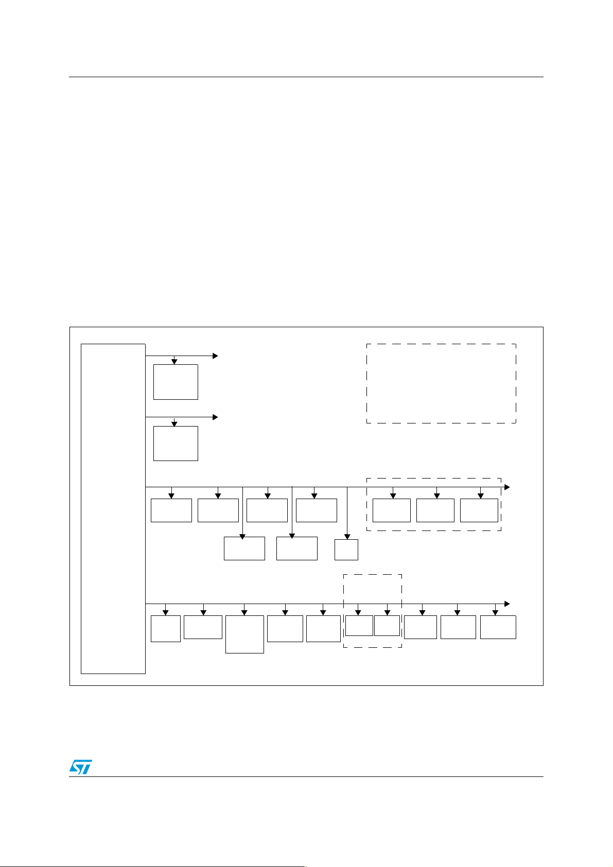
Figure 4. MC_ME mode diagram
SYSTEM MODES
software
request
RESET
non-recoverable
faliure
SAFE
DRUN
TEST
recoverable
hardware
failure
USER MODES
RUN0
HALT0
RUN1
RUN2
STOP0
RUN3
2.2 Modes description
2.2.1 System modes
RESET mode
This is a chip-wide virtual mode during which the application is not active.
The system remains in this mode until all resources are available for the embedded software
to take control of the device. It manages hardware initialization of chip configuration, voltage
regulators, oscillators, PLLs, and Flash modules.
DRUN mode
This is the entry mode for the embedded software.
It provides full accessibility to the system and enables the configuration of the system at
startup. It provides the unique gate to enter USER modes.
STANBY0
10/42 Doc ID 18232 Rev 1
Page 11

AN3316 Device modes
SAFE mode
This is a chip-wide service mode which may be entered on the detection of a recoverable
error. It forces the system into a pre-defined safe configuration from which the system may
try to recover.
TEST mode
This is a chip-wide service mode which is intended to provide a control environment for
device self-test. It may enable the application to run its own self-test like Flash checksum.
2.2.2 Running modes
RUNx (x=0:3) modes
These are software running modes where most processing activity is done. These modes
are intended to be used by software to execute full performance application routines.
The availability of 4 running modes allow to enable different clock and power configurations
of the system with respect to each other.
SPC560B device supports WAIT instruction to stop the core with the capability to restart
with very short latency (< 4 system clocks)
2.2.3 Low Power modes
HALT mode
This mode is intended as a first level low-power mode in which the platform is stopped but
system clock can remain the same as in running mode. This is a reduced-activity low-power
mode during which the clock to the core is disabled. It can be configured to switch off analog
peripherals like PLL, Flash, main regulator etc. for efficient power management at the cost
of higher wakeup latency.
STOP mode
This mode is intended as an advanced low-power mode during which the clock to the
platform is stopped. It may be configured to switch off most of the peripherals including
oscillator for efficient power management at the cost of higher wakeup latency.
STANBY mode
This is a reduced-leakage low-power mode in which only PD0 is connected and power
supply is cut off from most of the device. Wakeup from this mode takes a relatively long time,
and content is lost or must be restored from backup.
Doc ID 18232 Rev 1 11/42
Page 12

Device modes AN3316
Figure 5. Power Domain 0 architecture
LV
HV
API/
RTC
Wake-up
Logic
RESET &
Wake-up
vector
128KHz
IRC
16 MHz
IRC
2.3 Key advantages of Mode Entry
The purpose of the Mode Entry (ME) is to centralize the control of all device modes and
related parameters within a unique module.
Following main advantages:
● Controls the target mode’s parameters and mode transition without CPU intervention
(see Section 2.3.1: Transition control)
● Power modes managment centralaized (see Section 2.3.2: Modules/peripherals
configuration)
● Provides a SAFE mode to manage HW failure (see Section 2.3.3: HW failure and error
modes management)
Part of
Magic carpet
PCU
RGM 8K
RAM
32KHz
XTAL
PD0
(Always On
domain)
CAN
Sampler
2.3.1 Transition control
Mode transition is performed by writing ME_MCTL register twice:
● 1st write: TARGET_MODE + KEY
● 2nd write: TARGET_MODE + INVERTED KEY
Once the double writing is done, the complete transition could be triggered by following bits:
● S_MTRANS bit of Global Status Register (ME_GS)
– S_MTRANS = 0 (Transition not active)
– S_MTRANS = 1 (Transition ongoing)
● I_MTC bit of Interrupt Status Register (ME_IS)
– I_MTC = 0 (No transition complete)
– I_MTC = 1 (Transition complete)
Note: Bit I_MTC is not set in case of transition to low power modes (HALT / STOP)
2.3.2 Modules/peripherals configuration
Either modules or peripherals are managed by ME.
12/42 Doc ID 18232 Rev 1
Page 13
AN3316 Device modes
Modules management
Each mode has a configuration register (ME_XXX_MC) that allows to configure the
following modules:
● Output Configuration
For some modes it is possible to put the IO in power-down status (PDO), forcing
outputs of pads to high impedance state or switching off the pads’ power sequence
driver
● Main Voltage Regulator (MVREG) Configuration
For some modes it is possible to switch-off the MVREG in order to minimize the
consumption
● FLASHs Configuration
For some modes it is possible to configure the code and data Flash in normal, low
power and power down
● Clocks Configuration
ME module is in charge of:
– Main XOSC switching on/off
– IRC fast switching on/off
– FMPLL switching on/off
– System Clock selecting
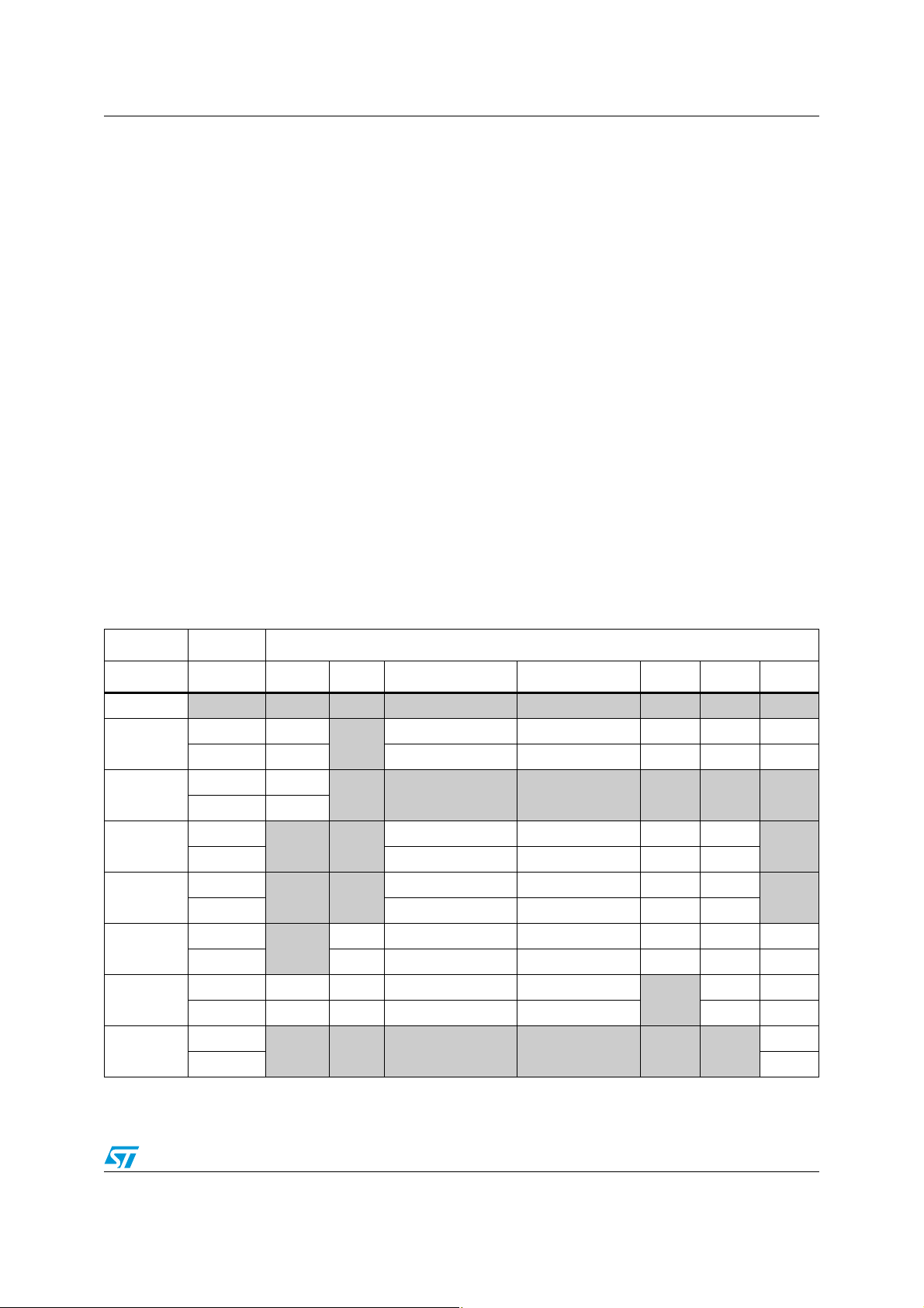
Not all modules can be configured in each mode. Following a table that describes all the
possible modules configurations for each mode:
Table 1. Module configuration
Mode PDO MVR DATA FLASH CODE FLASH PLL OSC IRC
RESET
TEST
SAFE
DRUN
RUNx
HALT
STOP
STBY
1. √ : module configurable
gray cell: module not configurable
Reset Off On Normal Normal Off Off On
User √
Reset Off Normal Normal Off Off On
User √
Reset On
User
Off On
Reset Normal Normal Off Off
User
Off On
Reset Normal Normal Off Off
User
Off
Reset On Low Power Low Power Off Off On
User √√ √ √
Reset Off On Power Down Power Down Off On
User
Off Off Power Down Power Down Off Off
Reset On
(1)
Module
√√√√√
On
On Normal Normal Off Off On
√√√√
√√√√
√√ √√√√
√√
Off
On
On
√
Doc ID 18232 Rev 1 13/42
Page 14

Device modes AN3316
Moreover, following table describes the possible system clock configurations for each mode:
Table 2. Clock configuration
System
RESET TEST SAFE DRUN HALT STOP STBY
IRC DEFAULT DEFAULT DEFAULT DEFAULT DEFAULT DEFAULT
IRC_DIV √ √√√
XOSC √ √√√
XOSC_DIV √ √√√
PLL √ √√
NO CLK √ √ DEFAULT
1. √ : module configurable
gray cell: module not configurable
(1)
Mode
Following an example that describes how to manage module configuration
● Current mode: Drun with system clock = IRC (default)
● Target mode: RUN0 mode with system clock = XOSC
Steps
● Configuration of RUNO mode
– ME_RUN0_MC.OSCON = 1
– ME_RUN0_MC.SYSCLK = XOSC
● Transition request
– ME_MCTL = DRUN + KEY
– ME_MCTL = DRUN + INVERTED KEY
● Waiting for the transition complete through the ME_IS.I_MTC bit
Figure 6. Mode transition example
DRUN RUN0
sysclk = IRC
sysclk = XOSC
14/42 Doc ID 18232 Rev 1
Page 15

AN3316 Device modes
Peripherals management
Each peripheral clock source can be switched on or off independently when it is not used, to
optimize power consumption. The ME module manages the clock gating of each peripheral,
defining peripherals state (active/frozen) in each mode as following:
● 8 Running registers (ME_RUN_PC[0..7]) to generate 8 different configuration in
running modes
● 8 Low-Power registers (ME_LP_PC[0..7]) to generate 8 different configuration in low
power modes
● One register for each peripheral (ME_PCTL[x]) that address one of the Running
configuration and one of the Low-Power configuration
Following is an example that describes how to clock gate/enable EMIOS peripheral:
Mode Entry - example
EMIOS0 Clock Gating
● Configure EMIOS in the following way
– Active in DRUN, RUN0, STOP mode
– Clock Gated in the others mode
Steps
● Configuration of Running mode
– ME_RUN_PC[1].DRUN = 1
– ME_RUN_PC[1].RUN0 = 1
● Configuration of Low Power mode
– ME_LP_PC[2].STOP = 1
● Configuraion of EMIOS (peripheral number = 72)
– ME_PTCL[72].RUN_CFG = 1
– ME_PTCL[72].LP_CFG = 2
Figure 7. Peripheral configuration example
DRUN
EMIOS active
STOP
Doc ID 18232 Rev 1 15/42
RUN0
Page 16

Device modes AN3316
2.3.3 HW failure and error modes management
ME Provides a SAFE mode to manage either HW failure or errors caused by incorrect mode
transition configurations.
HW failure management
Device can manage some HW failure events to force SAFE mode transition instead of
generating a reset. This is possible through RGM (Reset Generation Module), which, for
examples, allows to configure following less-critical functional events:
● FMPLL failure
● FXOSC failure
● CMU clock frequency higher/lower than reference
● 4.5 V low-voltage detected
● code or data Flash fatal error
So, if one of these happens, the system enters into a pre-defined SAFE configuration from
which it may try to recover. It is also possible that SAFE transition is triggered by an interrupt
through the ME.
Following is an example that describes how crystal failure event can be managed:
Example
● Current mode: DRUN with system clock = IRC (default)
● Target mode: RUN0 mode with system clock = XOSC
● XOSC failure event hapens
Steps
● Configuration of RUN0 mode
– ME_RUN0_MC.OSCON = 1
– ME_RUN0_MC.SYSCLK = XOSC
● Configuration of XOSC failure as SAFE transtition
– ME_RGM_FERD.D_CMU_OLR = 1
– ME_RGM_FEAR.AR_CMU_OLR = 0
● Configuration of SAFE mode interrupt
– ME_IM.M_SAFE = 1
● XOSC failure event hapens
● Software Transition request
– ME_MCTL = RUN0 + KEY
– ME_MCTL = RUN0 + INVERTED KEY
● SAFE mode transition forced and interrupt generated
16/42 Doc ID 18232 Rev 1
Page 17

AN3316 Device modes
Figure 8. HW failure example
SAFE
XOSC failure
svsclk = IRC
DRUN RUN0
svsclk = IRC svsclk = XOSC
Error modes management
Mode Entry Module can generate an interrupt on the following events:
● Invalid mode configuration:
following rules should be respected in order to prevent error configuration event:
– IRC should be ON if: sysclk = rc_clk or sysclk = rc_clk_div
– XOSC should be ON if: sysclk = osc_clk or sysclk = osc_clk_div
– PLL should be ON if: sysclk = pll_clk
– Configuration "00" for the CFLAON and DFLAON bit fields should not be used
– MVR must be ON if any of the following is active: PLL/CFLASH/DFLASH
– System clock configurations marked as ’reserved’ may not be selected
– Configuration "1111" for the SYSCLK bit field is allowed only for STOP0 and TEST
modes
If one of the previous rule is violated, I_ICONF bit in the Interrupt Status register ME_IS is
set
● Invalid mode transition
Following cases should be avoided to complete the transition properly:
– Mode requested when a transition is active (mode transition illegal)
– Target mode not valid with respect to the current (mode request illegal)
– Target mode is disabled in mode enable register (disable mode access)
– Target mode doesn’t exist (non existing mode access)
previous cases are signaled by ME_IMTS register.
2.4 Application cases
This chapter tries to show most significant transition cases managed by mode Entry
Module.
Except for the Power-On Reset phase that is performed through a completely HW transition
(RESET → DRUN), transitions have either HW or SW aspects in the others cases.
Doc ID 18232 Rev 1 17/42
Page 18

Device modes AN3316
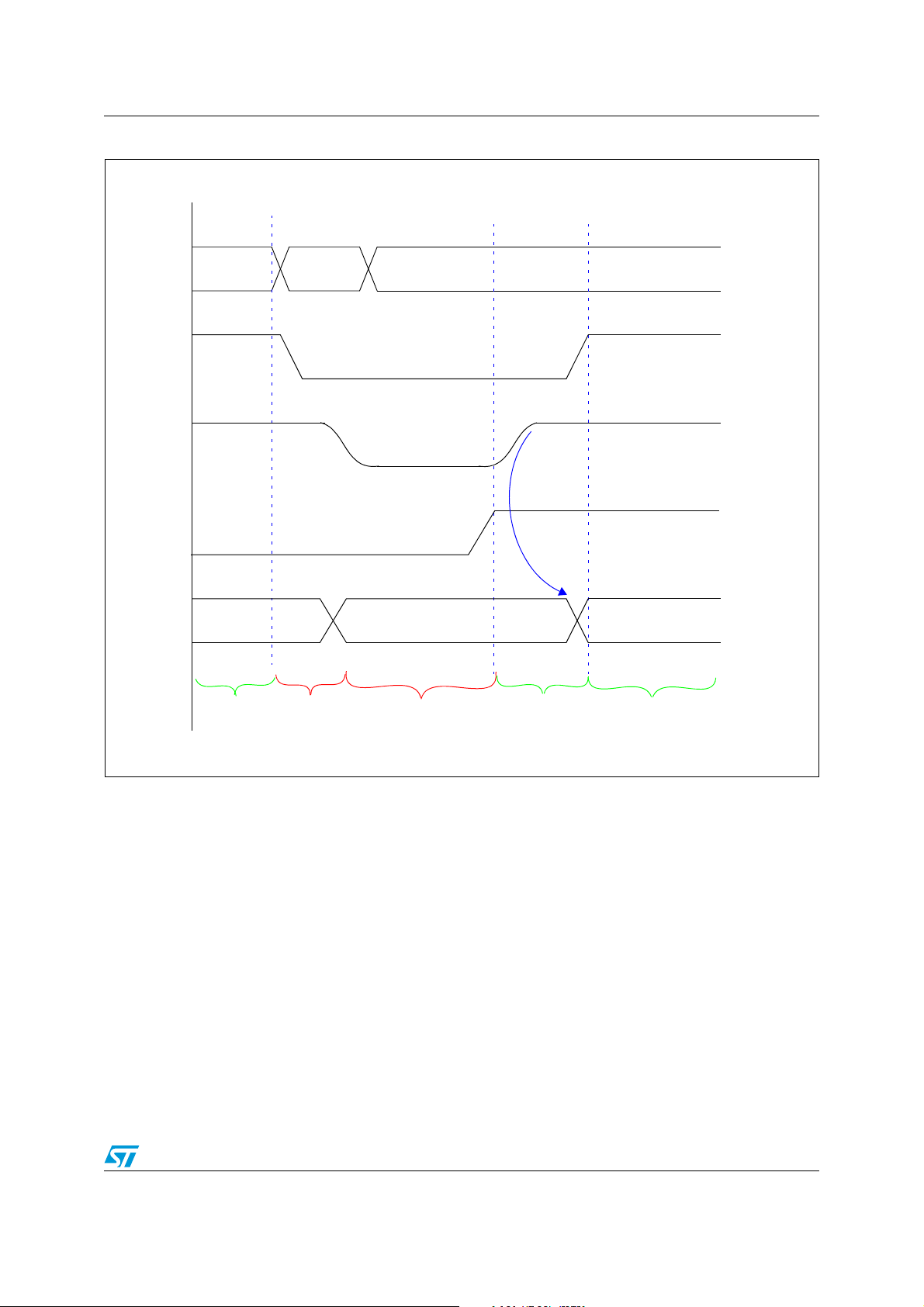
2.4.1 Power-on reset phase (RESET → DRUN)
Following, a chart that describes the start-up phase from CFLASH:
Figure 9. Transition (HW start-up) RESET → DRUN (execution from CFlash)
CORE
MODE
IRC 16M
VREG
RESET
(dig.)
STRAT-UP
SEQUENCE
Power-On
Reset
GATED POWERED
RESET
STOP RUNNING
ULTRA LP LOW POWER FULL POWER
ULP-VREGI
SET-UP
10
μ
s
IRC
LVD & MVREG
16M
μ
s
2
33
μ
s
Stabilize Flash
analog supply
20
μ
s
initialization
CFLASH
125
EXECUTE
DRUN
ME
μ
s
5
μ
s
Transition time: ~200
500mA(max)
Transition time: 200
Average conso: ~26mA
CONSUMPTION
PROFILE
25
μ
A
~5mA ~30mA
2.4.2 Application scenarios
The following scenarios shown are the typical ones that well describes the behavior of both
running and low power modes.
18/42 Doc ID 18232 Rev 1
μ
s
μ
s
~20mA
Page 19

AN3316 Device modes
Common HW aspects
As already said, other than sw configuration that should be taken care by the application,
there are some operations that are performed by HW and that are common to the scenarios
after described:
● <target mode> configuration check
While programming the mode configuration registers ME_<target mode>_MC, some rules
must be respected.
For example, if PLL is set to be the system clock in <target mode>, PLL should be turned
on. Otherwise, the write operation is ignored and an invalid mode configuration event may
be generated. Please refer to Error Management Chapter for detailed informations.
● <target mode> transition parameters check
There are some conditions that make the transition request invalid. For example, if the target
mode is not a valid mode with respect to current mode.
In this case, an invalid mode transition event may be generated. Please refer to Error
Management Chapter for detailed informations.
● <target mode> modules/peripherals switching on/off
Once the transition is requested by sw, the HW is in charge of switching on/off all
modules/peripherals. Now, if a module failure happens (i.e: XTAL or PLL lock failures) the
transition stalls in an ongoing status. However, The failures can be managed via software.
Please refer to Error Management Chapter for detailed informations.
For this reason, in order to prevent to stuck the code waiting for transition completion, it
could be better to set a timer, before entering in RUN0 mode, that, if expired, is able to signal
every potential issue.
Timeout calculation should be based on modules/peripherals start-up timing and, so, varies
case by case.
Scenario 1 (DRUN → RUNx)
This scenario is a typical application that starts from a default mode and transits to a full
device performance user mode. Following is the configuration of each mode.
Figure 10. Node configuration
DRUN RUN0
XTAL, PLL = OFF
sysclk = FIRC-16MHz
CFLASH, DFLASH = ON
all periphs = OFF
Following flow diagram describes the transition steps:
XTAL, PLL = OFF
sysclk = PLL-64MHz
CFLASH, DFLASH = ON
SPIO,ADCO = ON
Doc ID 18232 Rev 1 19/42
Page 20

Device modes AN3316
Figure 11. Transition step
DRUN Mode
DRUN Mode
1
XTAL Config
FMPLL config
2
3
mode config
periphs
4
mode config
Timer config
5
Request
6
transition to
RUN0
Application
HW
RUN0 config
check
Transi tion
DRUN → RUN0
7
RUN0 Mode
8
RUN0 Transition parameter
check
RUN0 switching on/off
modules/peripherals
N
Transition done?
Y
N
Time
expired?
Y
Error
management
RUN0 Mode
20/42 Doc ID 18232 Rev 1
Page 21

AN3316 Device modes
For the HW steps, refer to Section : Common HW aspects. Now, see in details the
operations done for each phase:
DRUN mode:
1. XTAL config
– CGM.OSC_CTL.EOCV = xxx (set stabilization counter)
2. FMPLL config:
PLL freq is done by the following formula:
phi
Where:
– clkin = reference clock = XTAL at 8 MHz
– LDF (NDIV) is the Loop Divided Ratio with this configurations:
Table 3. Loop divide ratio
NDIV[6:0] Loop divide ratios
0000000-0011111 NA
0100000 Divide by 32
0100001 Divide by 33
clkin LDF⋅
-----------------------------=
IDF ODF⋅
0100010 Divide by 34
... ...
1011111 Divide by 95
1100000 Divide by 96
1100001-1111111 NA
– IDF is the Input Divided Ratio with following configurations:
Table 4. Input divide ratio
IDF[3:0] Input divide ratios
0000 Divide by 1
0001 Divide by 2
0010 Divide by 3
... ...
1110 Divide by 15
– ODF is the Output Divided Ratio with following configurations:
Doc ID 18232 Rev 1 21/42
Page 22

Device modes AN3316
Table 5. Output divide ratio
ODF[1:0] Output divide ratios
00 Divide by 2
01 Divide by 4
10 Divide by 8
11 Divide by 16
So, to get PLL freq = 64MHz, in case of XTALat8MHz, registers configuration should
be:
CGM.FMPLL[0].CR.B.IDF = 0 (divide by 1)
CGM.FMPLL[0].CR.B.ODF = 2 (divide by 8)
CGM.FMPLL[0].CR.B.NDIV = 64 (multiply for 64)
3. RUN0 mode config:
ME_RUN0_MC.XOSC0ON = 1 (turn-on the XTAL)
ME_RUN0_MC.PLL0ON = 1 (turn-on the PLL)
ME_RUN0_MC.SYSCLK = 4 (set PLL as device system clock)
4. Periphs mode config:
ME_RUN_PC0.RUN0 = 1 (activate running peripheral configuration ’0’ in RUN0)
ME_PCTL[4].RUN_CFG = 0 to select the running peripheral configuration ’0’ for DSPI0
identified by offset = 4 (refer to figure x)
ME_PCTL[32].RUN_CFG = 0 to select the running peripheral configuration ’0’ for ADC
identified by offset = 32 (refer to figure x)
Table 6. SPC560B54/6x peripheral clock sources
Peripheral
RPP_ZOH platform None (managed through ME mode) —
DSPin 4+n 2
FlexCANn 16+n 2
BAM None (31 reserved) —
ADC 32 3
Register gatin address offset
(base = 0xC3FDC0C0)
Peripheral set
5. Timer config:
See Step 7 (DRUN → RUN0 mode)
22/42 Doc ID 18232 Rev 1
Page 23

AN3316 Device modes
6. Request transition to RUN0 mode:
The transition from a mode to another is handled by software by accessing the mode
control ME_MCTL register twice by writing:
– the first time with the value of the key (0x5AF0) into the KEY bit field and the
required target mode into the TARGET_MODE bit field
– the second time with the inverted value of the key (0xA50F) into the KEY bit field
and the required target mode into the TARGET_MODE bit field.
So, in case of DRUN → RUN0 transition, these two register writing should be done:
ME.MCTL.R = 0x40005AF0
ME.MCTL.R = 0x4000A50F
7. DRUN → RUN0 mode:
Once a valid mode transition request is detected, the transition starts. Here, device
switches-on/off modules and peripherals without CPU intervention.
It is possible to check for transition completion through mode Transition Status bit:
While (ME.GS.MTRANS != 0) //transition ongoing
... //transition completed
...
In ordeI to prevent code stucking waiting for transition completion, it could be better to
check transition timing through a timer. Timer timeout calculation should be based on
modules/peripherals start-up timing. In this case this value is close to XTAL start-up
time (at maximum 6 msec).
8. RUN0 mode:
Otherwise, if transition completion is signaled by sw, the RUN0 is properly entered with
the modules configured as expected.
Scenario 2 (RUN0 → HALT → RUN0)
This scenario deals with HALT mode that is the only one allowing to reduce average
consumption while the application is 100% functional. In fact, reducing dynamic
consumption through core switching-off and togheter with maintaining the full functionality is
one of the new challenge in body.
Figure 12. Scenario 2 - finite state machine
Software triggered transition
RUN0 HALT
Hardware triggered transition
XTAL, PLL = ON
sysclk = PLL-64MHz
CFLASH = ON
DFLASH = Low Power
SPI0, ADC0 = ON
XTAL, PLL = ON
sysclk = PLL-64MHz
CFLASH = Low Power
DFLASH = Low Power
SPI0, ADC0 = ON
CAN0 = ON
Doc ID 18232 Rev 1 23/42
Page 24

Device modes AN3316
Figure 13. Scenario 2 - flow chart
Application HW
Application HW
RUN0 Mode
RUN0 Mode
RUN0 Mode
RUN0 Mode
HALT Mode
1 HALT Mode
1
config
periphs config
periphs config
2
2
in HALT Mode
in HALT Mode
3
3
timer config
timer config
Request
4
4
transition to
transition to
HALT Mode
HALT Mode
config
Request
HALT config check
HALT config check
HALT transition parameter
HALT transition parameter
check
check
Transition
Transi tion
RUN0 -> HALT
RUN0 → HALT
5
5
HALT Mode
HALT Mode
6
6
CAN0
CAN0
interrupt event
interrupt event
Transition
Transi tion
HALT -> RUN0
HALT → RUN0
7
7
Transition
Tr an s i ti o n
done?
done?
HALT Mode
HALT Mode
NN
NN
Time
Time
expired?
expired?
YY
YY
Error
Error
management
management
HALT switching
HALT switching
ON/OFF modules/
ON/OFF modules/
peripherals
peripherals
-RUN0 transition
-RUN0 transition
parameter check
parameter check
-RUN0 switching on/off
-RUN0 switching on/off
modules/periphs
modules/periphs
RUN0 Mode
RUN0 Mode
RUN0 Mode
8
8
24/42 Doc ID 18232 Rev 1
RUN0 Mode
Page 25

AN3316 Device modes
For the HW steps, refer to Section : Common HW aspects. Now, see in details the operation
done for each phase:
RUN0 mode:
1. Mode config in HALT:
ME_HALT_MC.CFLAON = 2 (code Flash in Low Power mode)
ME_HALT_MC.DFLAON = 2 (data Flash in Low Power mode)
In this way, at HALT exiting, Flash startup from Low Power to Normal mode is very fast
as it takes less than 1 usec
ME_ HALT_MC.XOSC0ON = 1 (turn-on the XTAL)
ME HALT_MC.PLL0ON = 1 (turn-on the PLL)
ME_ HALT_MC.SYSCLK = 4 (set PLL as device system clock)
2. Periphs mode config HALT mode:
ME_RUN_LP0.HALT = 1 (activate low power peripheral configuration ’0’ in HALT)
ME_PCTL[4].LP_CFG = 0 to select the low power peripheral configuration ’0’ for
DSPI0 identified by offset = 4 (refer to figure x)
ME_PCTL[32].LP_CFG = 0 to select the low power peripheral configuration ’0’ for ADC
identified by offset = 32 (refer to figure x)
ME_PCTL[16].LP_CFG = 0 to select the low power peripheral configuration ’0’ for
FlexCAN0 identified by offset = 16 (refer to figure x)
Table 7. Peripherals clock source
Peripheral
RPP_ZOH Platform
DSPin 4 + n 2
FlexCANn 16 + n 2
BAM None (31 reserved) —
ADC 32 3
Register gatin address offset
(base = 0xC3FDC0C0)
None (managed through ME
mode)
Peripheral set
—
3. Timer config:
See Step 5 (RUN0 → HALT mode)
4. Request transition to RUN0 mode:
So, in case of RUN0 → HALT transition, these two register writing should be done:
ME.MCTL.R = 0x80005AF0
ME.MCTL.R = 0x8000A50F
Doc ID 18232 Rev 1 25/42
Page 26

Device modes AN3316
5. RUN0 → HALT mode:
Once a valid mode transition request is detected, the transition starts. Here, device
switches-on/off modules and peripherals without CPU intervention.
It is possible to check for transition completion through mode Transition Status bit:
while (ME.GS.MTRANS != 0) //transition ongoing
... //transition completed
in order to prevent code stucking waiting for transition completion, it could be better to
check transition timing through a timer. Timer timeout calculation should be based on
modules/peripherals start-up timing. As, in this case, as there aren’t any slow-start-up
peripherals to switch-on, timeout could be considered equal to few clock cycles.
6. HALT mode:
At the end of the transition, device enters in HALT mode with core switched-off,
FlexCAN0 switched-on and CFLASH in Low Power mode. All others peripherals are
maintained in the same status of the RUN0 mode.
As already said, the advantage of this configuration is that core switching-off allows to
reduce average consumption while the application is still 100% functional.
At this point, if a FlexCAN0 interrupt event is generated, the device, automatically,
starts the transition to go back to the previous RUN0
7. Transition HALT → RUN0 mode:
During the HALT → RUN0 transition, the device automatically restores the
peripherals/modules as they were configured before entering in HALT. So, core is
already on and CFLASH comes back to Normal mode
8. RUN0 mode:
At the end of the transition, device enters in RUN0 mode with initial configuration
Scenario 3 (RUN0 → STOP → RUN0)
This scenario is a typical transition from the application when going from
Running → Standby when the car is switched off. However, the application does not go
directly to the lowest consumption STANDBY mode but rather in 2 or even 3 steps. And here
STOP could be the last step before STANDBY where the application still monitor for a
certain time the activity in the vehicle.
Figure 14. Scenario 3 - finite state machine
Software triggered transition
RUN0 STOP
Hardware triggered transition
XTAL, PLL = ON
sysclk = PLL-64MHz
CFLASH = ON
DFLASH = Low Power
CAN0 = ON
XTAL, PLL = ON
PLL = OFF
sysclk = FIRc-16MHz
CFLASH = Power Down
DFLASH = Low Power
CAN0 = ON
26/42 Doc ID 18232 Rev 1
Page 27

AN3316 Device modes
Figure 15. Scenario 3 - flow chart
Application HW
Application HW
RUN0 Mode
RUN0 Mode
RUN0 Mode
RUN0 Mode
STOP Mode
1
1 HALT Mode
config
config
STOP config check
HALT config check
periphs config
periphs config
2
2
in STOPMode
in HALT Mode
3
3
timer config
timer config
Request
Request
4
4
transition to
transition to
STOP Mode
HALT Mode
STOP transition parameter
HALT transition parameter
check
check
Transi tion
Transition
RUN0 → STOP
RUN0 -> HALT
5
5
STOP Mode
HALT Mode
6
6
CAN0
CAN0
interrupt event
interrupt event
Transition
Transi tion
HALT -> RUN0
STOP → RUN0
7
7
Tr an s i ti o n
Transition
done?
done?
STOP Mode
HALT Mode
NN
NN
Time
Time
expired?
expired?
YY
YY
Error
Error
management
management
STOP switching
HALT switching
ON/OFF modules/
ON/OFF modules/
peripherals
peripherals
-RUN0 transition
-RUN0 transition
parameter check
parameter check
-RUN0 switching on/off
-RUN0 switching on/off
modules/periphs
modules/periphs
RUN0 Mode
RUN0 Mode
8
8
RUN0 Mode
RUN0 Mode
Doc ID 18232 Rev 1 27/42
Page 28

Device modes AN3316
For the HW steps, refer to Chapter : Common HW aspects. Now, see in details operation
done for each phase:
RUN0 mode:
1. Mode config in STOP:
ME_STOP_MC.CFLAON = 1 (code Flash in Power-Down)
ME_STOP_MC.DFLAON = 2 (data Flash in Low Power mode)
In this way, at STOP exiting, Flash startup from Power-Down to Normal mode takes few
usecs
ME_ STOP_MC.XOSC0ON = 1 (turn-on the XTAL)
The XTAL is maintained on in STOP in order to clock CAN protocol handler: in this way
PLL jitter issues are avoided
ME_ STOP_MC.SYSCLK = 0 (set FIRC as device system clock)
2. Periphs mode config STOP mode:
ME_RUN_LP0.STOP = 1 (activate low power peripheral configuration ’0’ in STOP)
ME_PCTL[16].LP_CFG = 0 to select the low power peripheral configuration ’0’ for
FlexCAN0 identified by offset = 16 (refer to figure x)
3. Timer config:
See Step 5 (RUN0 → HALT mode)
4. Request transition to RUN0 mode:
in case of RUN0 → STOP transition, these two register writing should be done:
ME.MCTL.R = 0xA0005AF0
ME.MCTL.R = 0xA000A50F
5. RUN0 → STOP mode:
Once a valid mode transition request is detected, the transition starts. Here, device
switches-on/off modules and peripherals without CPU intervention.
It is possible to check for transition completion through mode Transition Status bit:
while (ME.GS.MTRANS != 0) //transition ongoing
... //transition completed
...
in order to prevent code stucking waiting for transition completion, it could be better to
check transition timing through a timer. As, in this case, as there aren’t any slow-startup peripherals to switch-on, timeout could be considered equal to few clock cycles.
6. STOP mode:
At the end of the transition, device enters in STOP mode with core switched-off,
FlexCAN0 switched-on and CFLASH in Power Down. All others peripherals are
maintained in the same status of the RUN0 mode.
At this point, if a FlexCAN0 interrupt event is generated, the device, automatically,
starts the transition to go back to the previous RUN0
7. transition STOP → RUN0 mode:
During the STOP → RUN0 transition, the device automatically restores the
peripherals/modules as they were configured before entering in STOP. So, core is
already on and CFLASH comes back to Normal mode
28/42 Doc ID 18232 Rev 1
Page 29

AN3316 Device modes
8. RUN0 mode:
At the end of the transition, device enters in RUN0 mode with initial configuration
Scenario 4 (RUNx → STANDBY → RUNx)
This scenario is a typical application that remains in STANDBY for most of time minimizing
at maximum the power consumption and wakeup periodically to execute some operations
(for example ADC acquisition).
Figure 16. Scenario 4 - finite state machine
Software triggered transition
RUN0
Hardware triggered transition
XTAL, PLL = ON
sysclk = PLL-64MHz
CFLASH = ON
DFLASH = Low Power
STANBY
FIRC, sysclk = ON
SIRC = ON
RAM size = 8 KB
CFLASH = Power Down
periodic wakeup with API
booting from RAM
Doc ID 18232 Rev 1 29/42
Page 30

Device modes AN3316
Figure 17. Scenario 4 - flow chart
HWApplication
RUN0 Mode
Transition
RUN0 → STBY
5
RUN0 Mode
STBy Mode
1
config
booting
config in
2
STBY Mode
3
API config
Request
transition to
4
STBY Mode
STBY config check
STBY config parameter
check
STBY switching on/off
modules/peripherals
STBY Mode
6
STBY Mode
Transition
STBY → RESET → DRUN
7
DRUN Mode
8
DRUM Mode
(in RAM)
period
NAPI
expired?
Y
-Request sequence
-DRUN Mode entering
30/42 Doc ID 18232 Rev 1
Page 31

AN3316 Device modes
For the HW steps, refer to Section : Common HW aspects. Now see in details the operation
done for each phase:
RUN0 mode:
1. Mode config in STDBY:
STANDBY mode, by default has already following configuration:
– CFLASH/DFLASH in Power Down
–XTAL OFF
– Sysclk OFF
So, the only sw configurations to perform are:
ME_ STANDBY_MC.FIRCON = 0 (turn-off the FIRC)
CGM_ LPRC.LPRCON_STDBY = 1 (turn-on the LPRC in STANDBY)
Moreover, it needs that all peripherals are clock-gated, otherwise, STANDBY mode is
not entered properly, so:
ME_ RUN_LPx.STANDBY = 0 (all low power peripheral configuration registers used
should have STANDBY disabled)
2. STDBY Boot config:
RGM_STDBY.BOOT_FROM_BKP_RAM = 1 (boot from SRAM on STANDBY exit)
ME_DRUN_MC.CFLAON = 1 (code Flash in Power-Down)
PCU_PCONF2.STDBY0 = 0 (SRAM 24K powered-off)
with these settings, after exiting from STANDBY, device enters in DRUN booting from
SRAM (8K backup) with CFLASH in Power-Down, minimizing consumption
3. API config:
This step should configure the API to generate a periodic wakeup to exit device from
STANDBY
4. Request transition to RUN0 mode:
in case of RUN0 → STANDBY transition, these two register writing should be done:
ME.MCTL.R = 0xD0005AF0
ME.MCTL.R = 0xD000A50F
5. RUN0 → STANDBY mode:
Once a valid mode transition request is detected, the transition starts. Here, device
switchs-off core and all the modules/peripherals that belong to Power-Domain #1. Only
Power-Domain #2 is maintained on.
Doc ID 18232 Rev 1 31/42
Page 32

Device modes AN3316
Figure 18. Power domain
PCON
F1[new mode]
new mode
wakeup
PCON
F2[new mode]
new mode
wakeup
Determine new
power state
Determine new
power state
power down
power up
power down
power up
PCU
SRAM (8K), Power Control Unit(PCU), RESET
Generation Module(RGM), Voltage regulator.
Wakeup Unit, API, CAN sampler, 16MHz & 128
KHz RC oscillator, RC digital interface & voltage
FSN
FSN
Power domain #1
Core Flash
#1
#2
Supply
Peripheral
set #1
PLL0
Power Domain #2
SRAM(24KB)
VREG
2
ME
JTAG
...
Power Domain #0
Note:
represents a power switching device. For the sake of simplicity this has been drawn as a mechanical switch.
Ground
It is possible to check for transition completion through mode Transition Status bit:
while (ME.GS.MTRANS != 0) //transition ongoing
... //transition completed
...
No timer is used here to check for the transition completion as timers are switched-off
during RUN0 → STANDBY transition
6. STANDBY mode:
At the end of the transition, device enters in STANDBY and stay there until the API not
generates a wakeup event. At this time the STANDBY exiting starts
7. Transition STANDBY → RESET → DRUN mode:
Once the wakeup event is generated, the device re-executes the Power-On Reset
phase staying in RESET mode. At the end, device enters in DRUN mode, where the
DRUN configuration register resets except for the DRUN.CFLAON/DFLAON that
maintains the values configured before STANDBY entering. This allows to put
CFLASH/DFLASH in Power Down once in DRUN.
32/42 Doc ID 18232 Rev 1
Page 33
AN3316 Device modes
Figure 19. STANDBY transition
new mode
requested
by ME
PSTAT.PDI
voltage in
power
domain #1
RUNo STANBY0 mode set due to reset being asserted to power domain
#1
wakeup
request
current
mode
RUN0 STANBY0 DRUN
power-up
state
● 8 - DRUN mode:
powerdown
phase
power-down state power-up
phase
power-up state
At the end of the transition, device enters in DRUN mode fetching the code from the first
SRAM location (0x40000000).
Doc ID 18232 Rev 1 33/42
Page 34

Consumption tables AN3316
3 Consumption tables
The target is to show the consumption of Running and Low Power modes for different
configurations. These values should be based on Bol1.5M cut2.0 measurements.
3.1 Running mode
This table shows modules consumption contributions in running mode with following
features:
● Code: continuous data transfer from Flash to RAM
● fsys = system clock (MHz)
● code executing from Flash
● all peripherals gated
Table 8. RUN0 mode consumption table
IP Conso (mA)
FIRC-16MHz 0.6
FOSC-8MHz 1.78
PLL 0.0303 * fsys
Low Power Normal
0.89 7.22
Low Power Normal
0.6 4.29
RUN0
mode
CFLASH
DFLASH
MVREG 1.06
Platform + PD0 0.4434 * fsys + 0.7765
Where PDO = Power Domain 0
In this way, it is possible to calculate the total consumption related to a specific configuration
easily.
As an example, consider following configuration at fsys = 16 MHz:
34/42 Doc ID 18232 Rev 1
Page 35

AN3316 Consumption tables
Table 9. RUN0 mode consumption example
IP Status Formula (mA) Conso (mA)
FIRC-16MHz On 0.6 0.6
FOSC-8Mhz On 1.78 1.78
PLL On 0.0303 * fsys 0.4848
CFLASH Normal
RUN0 mode
DFLASH
MVREG
Platform + PD0 0.4434 * fsys + 0.7765 7.8709
Total conso evaluated 23.3057
Total conso measured 23.51
3.2 Low Power modes
Following tables show how to calculate low power modes (HALT/STOP/STANDBY)
consumption respectively, summing the contributions of each module
3.2.1 HALT consumption
This table shows modules consumption contributions in HALT mode:
Table 10. HALT mode consumption table
IP conso(mA)
Power
Down
Always On
Low Power Normal
7.22
0.89 7.22
Low Power Normal
4.29
0.6 4.29
1.06 1.06
FIRC-16MHz 0.6
FOSC-6MHz 1.78
PLL mA = 0.0303 * MHz
Low Power Normal
CFLASH
0.89 7.22
Low Power Normal
HALT mode
DFLASH
0.6 4.29
MVREG 1.06
(1)
PD0
(always on)
(2)
PDI
1. Core/Platform + Power Domain 0 (always On) consumption
2. Consumption of Power Domain 1 that depends on the system clock (divided or not) provided to the
pheripherals
mA = 0.0668 * MHz + 0.5791
mA = 0.2092 * MHz + 0.077
Doc ID 18232 Rev 1 35/42
Page 36

Consumption tables AN3316
So, the HALT lowest consumption is 1.21 mA obtained with following configuration:
– FIRC on → 0.6 mA
– sysclk = FIRC/32 → PD0 conso = 0.0668 * 0.5 + 0.5791
– all others modules/peripherals off
As an example, consider following HALT mode configuration with fsys = 64 MHz and all
peripherals clocked at 32 MHz
Table 11. HALT mode consumption example
IP Status Formula(mA) Conso(mA)
FIRC-16MHz On 0.6 0.6
FOSC-6MHz On 1.78 1.78
PLL On 0.0303 * fsys 1.9392
Low Power Normal
7.22
0.89 7.22
Low Power Normal
0
0.6 4.29
HALT mode
CFLASH Normal
DFLASH Power Down
MVREG On 1.06 1.06
(1)
PD0
(always on)
(2)
PDI
On mA = 0.0668*64 + 0.5791 4.8543
On mA = 0.2092*32 + 0.077 6.7714
Total conso evaluated 25.2249
Total conso measured 25.41
1. Core/Platform + Power Domain 0 (always On) consumption
2. Consumption of Power Domain 1 that depends on the system clock (divided or not) provided to the
pheripherals
3.2.2 STOP consumption
This table shows modules consumption contributions in STOP mode:
36/42 Doc ID 18232 Rev 1
Page 37

AN3316 Consumption tables
Table 12. STOP mode consumption table
IP Conso (mA)
FIRC-16MHz 0.6
FOSC-8MHz 1.78
PLL Non onfigurable
CFLASH
Low Power Normal
0.89 7.22
Low Power Normal
DFLASH
STOP mode
0.6 4.29
MVREG 1.06
Power-Down output 0.44
(1)
PD0
(2)
PD1
1. Core/Platform + Power Domain 0 (always on consumption
2. Consumption of Power Domain 1 that depends on the system clock (divided or not) provided to the
peripherals
0.0585*fsys + 0.2
0.194*fsys + 0.1978
So, the STOP lowest consumption is 0.2 mA obtained with following configuration:
– Sysclk off → PD0 conso = 0.2 mA
– all others modules/peripherals off
As an example, consider following STOP mode configuration with fsys = 8 MHz and all
peripherals clocked at 2 MHz:
Table 13. STOP mode consumption example
IP Status Formula(mA) Conso(mA)
FIRC-16MHz On 0.6 0.6
FOSC-8MHz Off 1.78 0
PLL Off Non Configurable 0
Low Power Normal
CFLASH Normal
0.89 7.22
Low Power Normal
DFLASH Power down
STOP mode
0.6 4.29
MVREG On 1.06 1.06
Power-Down Output On 0.44 0
(1)
PD0
PD1
(2)
0.194*2 + 0.1978 0.5858
Total conso evaluated 10.1338
Total conso measured 10.41
1. Core/Platform + Power Domain 0 (always on consumption
Doc ID 18232 Rev 1 37/42
7.22
0
0.0585*8 + 0.2 0.668
Page 38

Consumption tables AN3316
2. Consumption of Power Domain 1 that depends on the system clock (divided or not) provided to the
peripherals
3.2.3 STANDBY consumption
This table shows modules consumption contributions in STANDBY mode:
Table 14. STANDBY mode consumption table
IP conso (μA)
FIRC-16MHz 290
FOSC-8MHz OFF (not config)
PLL OFF (not config)
CFLASH Power Down (not config)
DFLASH Power Down (not config)
MVREG OFF (not config)
Power-Down output
STANBY mode
SIRC-128KHz 3
SRAM-24KB 0.8
PD0
PD1
(1)
(2)
ON (not config)
21 (not config)
OFF (not config)
1. Core/Platform + Power Domain 0 (always on consumption
2. Consumption of Power Domain 1 that depends on the system clock (divided or not) provided to the
peripherals
So, the STANDBY lowest consumption is 21 µA obtained with following configuration:
– PD0 conso = 0.2 mA
– FIRC,SIRC,SRAM-24K off
On the other hand, maximum consumption (FIRC,SIRC,SRAM-24K on) is 314.8 µA.
3.3 Peripherals
In order to evaluate peripheral consumption contributions measured on ballast voltage
(IDD_BV), following table can be used that provides for all the main device peripherals,
either dynamic or static consumption.
38/42 Doc ID 18232 Rev 1
Page 39

AN3316 Consumption tables
Table 15. Peripherals consumption table
Symbol C Parameter Conditions
500 Kbps Total (static + dynamic)
CAN
I
DD_BV(CAN)
CC T
(FlexCAN)
supply current
on V
DD_BV
125Kbps 8 * f
Static consumption:
– eMIOS channel OFF
IDD_BV(eMIOS) CC T
eMIOS supply
current on
V
DD_BV
– Global prescaler enabled
Dynamic consumption:
– It does not change by varying the frequency
(0.003 mA)
Total (static + dynamic) consumption:
– LIN mode
– Baudrate: 20 Kbps
I
DD_BV(SCI)
CC T
SCI(LINFlex)
supply current
on V
DD_BV
Ballast static condition (only clocked) 1
Ballast dynamic condition (continuous
communication):
– Baudrate: 2 Mbit
– Transimmisio every 8 s
I
DD_BV(SPI)
CC T
SPI(DSPI)
supply current
on V
DD_BV
– Frame: 16 bits
consumption:
– FlexCAN in loop-back mode
– XTAL at 8 MHz used as CAN
engine clocksource
– Message sending period is 580s
8 * f
29 * f
5 * f
16 * f
Value
Type
periph
periph
periph
3
periph
periph
Unit
+ 85
+ 27
μA
+ 31
V
DD = 5.5V
V
DD = 5.5V
V
DD = 5.5V
V
DD = 5.5V
I
DD_BV(ADC)
I
DD_HV_ADC(ADC)
CC T
CC T
ADC supply
current on
V
DD_BV
ADC supply
current on
V
DD_HV_ADC
3.4 Consumption example
So, to calculate the peripheral consumption refer to the following scenario:
● Fperiph = PLL at 32 MHz
● Fcan = XTAL at 8 MHz (to avoid PLL glitches)
Each peripheral is showed in the following table:
Ballast static consumption (no
conservation)
Ballast dynamic consumption
(continuous conservation)
Analog static consumption (no
conservation)
Analog dynamic consumption
(continuous conservation)
41 * f
5 * f
2 * f
75 * f
periph
periph
µA
periph
periph + 32
Doc ID 18232 Rev 1 39/42
Page 40

Consumption tables AN3316
Table 16. Peripherals consumption example
IP Formula (µA) Conso (mA)
2 x CAN at 500 Kbps 2 x (8 * Fcan + 85) 0.234
4 x eMIOS PWM at 200 Hz 29 * Fperiph + 3 0.931
4 x LIN at 20 Kbps 4 x (5 * Fperiph + 31) 0.764
3 x SPI at 2 Mbps 3 x (16 * Fperiph) 1.536
24 x ADC (continous conv.)
Total peripherals conso 4.937
46 * Fperiph 1.472
40/42 Doc ID 18232 Rev 1
Page 41

AN3316 Revision history
4 Revision history
Table 17. Document revision history
Date Revision Changes
17-Nov-2010 1 Initial release.
Doc ID 18232 Rev 1 41/42
Page 42

AN3316
Please Read Carefully:
Information in this document is provided solely in connection with ST products. STMicroelectronics NV and its subsidiaries (“ST”) reserve the
right to make changes, corrections, modifications or improvements, to this document, and the products and services described herein at any
time, without notice.
All ST products are sold pursuant to ST’s terms and conditions of sale.
Purchasers are solely responsible for the choice, selection and use of the ST products and services described herein, and ST assumes no
liability whatsoever relating to the choice, selection or use of the ST products and services described herein.
No license, express or implied, by estoppel or otherwise, to any intellectual property rights is granted under this document. If any part of this
document refers to any third party products or services it shall not be deemed a license grant by ST for the use of such third party products
or services, or any intellectual property contained therein or considered as a warranty covering the use in any manner whatsoever of such
third party products or services or any intellectual property contained therein.
UNLESS OTHERWISE SET FORTH IN ST’S TERMS AND CONDITIONS OF SALE ST DISCLAIMS ANY EXPRESS OR IMPLIED
WARRANTY WITH RESPECT TO THE USE AND/OR SALE OF ST PRODUCTS INCLUDING WITHOUT LIMITATION IMPLIED
WARRANTIES OF MERCHANTABILITY, FITNESS FOR A PARTICULAR PURPOSE (AND THEIR EQUIVALENTS UNDER THE LAWS
OF ANY JURISDICTION), OR INFRINGEMENT OF ANY PATENT, COPYRIGHT OR OTHER INTELLECTUAL PROPERTY RIGHT.
UNLESS EXPRESSLY APPROVED IN WRITING BY AN AUTHORIZED ST REPRESENTATIVE, ST PRODUCTS ARE NOT
RECOMMENDED, AUTHORIZED OR WARRANTED FOR USE IN MILITARY, AIR CRAFT, SPACE, LIFE SAVING, OR LIFE
SUSTAINING APPLICATIONS, NOR IN PRODUCTS OR SYSTEMS WHERE FAILURE OR MALFUNCTION MAY RESULT IN
PERSONAL INJURY, DEATH, OR SEVERE PROPERTY OR ENVIRONMENTAL DAMAGE. ST PRODUCTS WHICH ARE NOT
SPECIFIED AS "AUTOMOTIVE GRADE" MAY ONLY BE USED IN AUTOMOTIVE APPLICATIONS AT USER’S OWN RISK.
Resale of ST products with provisions different from the statements and/or technical features set forth in this document shall immediately void
any warranty granted by ST for the ST product or service described herein and shall not create or extend in any manner whatsoever, any
liability of ST.
ST and the ST logo are trademarks or registered trademarks of ST in various countries.
Information in this document supersedes and replaces all information previously supplied.
The ST logo is a registered trademark of STMicroelectronics. All other names are the property of their respective owners.
© 2010 STMicroelectronics - All rights reserved
STMicroelectronics group of companies
Australia - Belgium - Brazil - Canada - China - Czech Republic - Finland - France - Germany - Hong Kong - India - Israel - Italy - Japan -
Malaysia - Malta - Morocco - Philippines - Singapore - Spain - Sweden - Switzerland - United Kingdom - United States of America
www.st.com
42/42 Doc ID 18232 Rev 1
 Loading...