


AN3311
Application note
In-home display for ZigBee® smartplug
Introduction
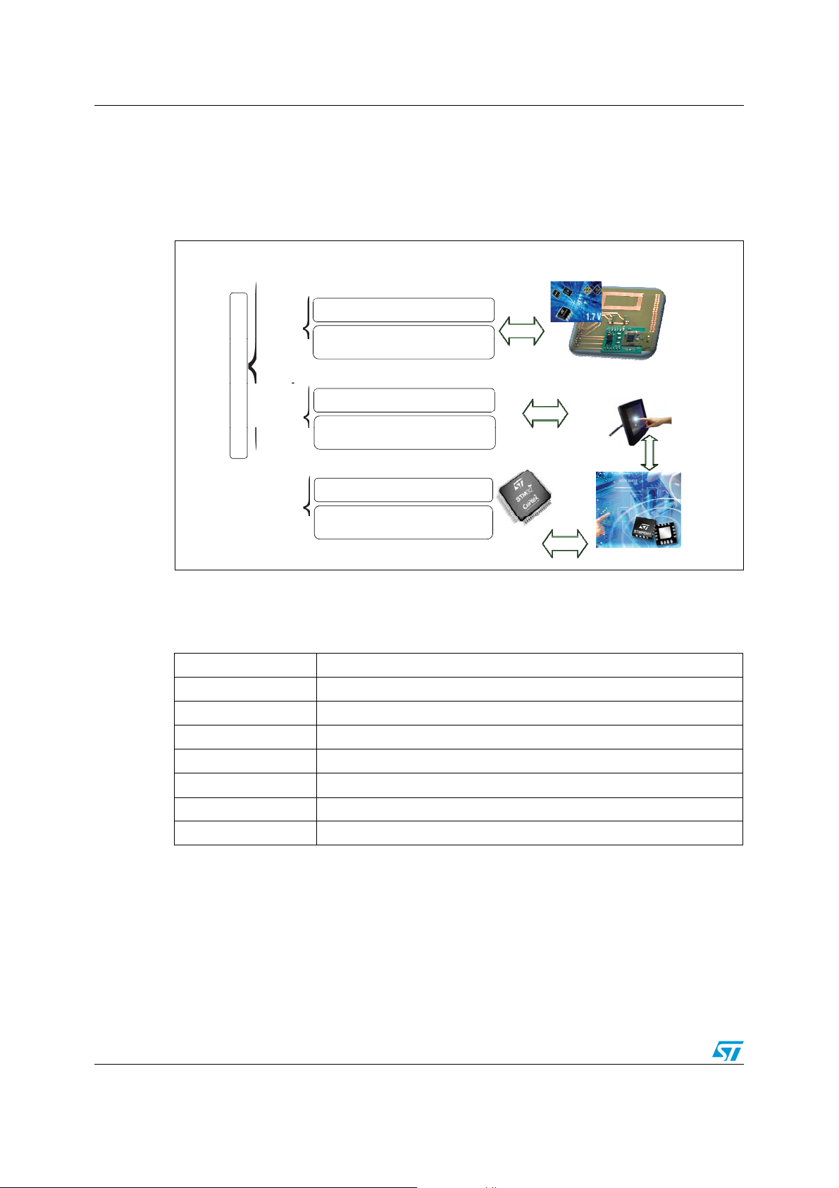
This application note describes the demonstration firmware running on the STM3210CEVAL for the STM32F107VC to manage a smartplug network system.
An embedded graphical user interface (GUI) based on the “multi-input embedded GUI
library 2.0 for STM32F10xxx” described in the AN3128 application note, and working on an
LCD TFT 320 x 240 display and 5-position joystick, allows the user to interact with the
smartplug system made up of one coordinator and two smartplugs connected.
Section 1 describes the document and library rules.
Section 2 highlights the features of the ZigBee smartplug and explains its hardware
interface with a device microcontroller (STM32).
Section 3 describes briefly the “multi-input embedded GUI library”.
Section 4 describes the relevant blocks of the STM3210C-EVAL demonstration board.
Section 5 shows the demonstration firmware/board system setup.
Section 6 describes, in detail, how the “in-home display” firmware is structured, its
architecture and its exported APIs.
Section 7 explains how to get started with the system, how to configure and use the IAR
workspace, and contains an example application source code.
Section 8 illustrates how the “in-home display” GUI application works.
Section 9 illustrates the hardware schematics.
December 2010 Doc ID 18209 Rev 1 1/58
www.st.com

Contents AN3311
Contents
1 Document and library rules . . . . . . . . . . . . . . . . . . . . . . . . . . . . . . . . . . . 6
1.1 Acronyms . . . . . . . . . . . . . . . . . . . . . . . . . . . . . . . . . . . . . . . . . . . . . . . . . . 6
2 ZigBee smartplug . . . . . . . . . . . . . . . . . . . . . . . . . . . . . . . . . . . . . . . . . . . 7
2.1 Smartplug description . . . . . . . . . . . . . . . . . . . . . . . . . . . . . . . . . . . . . . . . 7
2.2 ZigBee module . . . . . . . . . . . . . . . . . . . . . . . . . . . . . . . . . . . . . . . . . . . . . . 8
3 Multi-input embedded GUI library . . . . . . . . . . . . . . . . . . . . . . . . . . . . . . 9
3.1 Description . . . . . . . . . . . . . . . . . . . . . . . . . . . . . . . . . . . . . . . . . . . . . . . . . 9
4 STM3210C-EVAL demonstration board . . . . . . . . . . . . . . . . . . . . . . . . . 11
4.1 Features . . . . . . . . . . . . . . . . . . . . . . . . . . . . . . . . . . . . . . . . . . . . . . . . . . 12
4.2 STM32 peripherals mapping . . . . . . . . . . . . . . . . . . . . . . . . . . . . . . . . . . 12
4.3 Power supply . . . . . . . . . . . . . . . . . . . . . . . . . . . . . . . . . . . . . . . . . . . . . . 14
4.4 Boot option . . . . . . . . . . . . . . . . . . . . . . . . . . . . . . . . . . . . . . . . . . . . . . . . 15
4.5 Clock source . . . . . . . . . . . . . . . . . . . . . . . . . . . . . . . . . . . . . . . . . . . . . . . 16
4.6 Reset source . . . . . . . . . . . . . . . . . . . . . . . . . . . . . . . . . . . . . . . . . . . . . . 16
4.7 Joystick . . . . . . . . . . . . . . . . . . . . . . . . . . . . . . . . . . . . . . . . . . . . . . . . . . . 17
4.8 Pushbuttons . . . . . . . . . . . . . . . . . . . . . . . . . . . . . . . . . . . . . . . . . . . . . . . 17
4.9 Storage memory . . . . . . . . . . . . . . . . . . . . . . . . . . . . . . . . . . . . . . . . . . . . 17
4.10 Development and debug support . . . . . . . . . . . . . . . . . . . . . . . . . . . . . . . 17
4.11 Display and input devices . . . . . . . . . . . . . . . . . . . . . . . . . . . . . . . . . . . . . 17
4.12 JTAG debugging connector CN13 . . . . . . . . . . . . . . . . . . . . . . . . . . . . . . 18
4.13 Daughterboard extension connector CN8 and CN9 . . . . . . . . . . . . . . . . . 19
4.14 TFT LCD connector CN14 . . . . . . . . . . . . . . . . . . . . . . . . . . . . . . . . . . . . 23
4.15 Power connector CN18 . . . . . . . . . . . . . . . . . . . . . . . . . . . . . . . . . . . . . . 23
5 Demonstration firmware system setup . . . . . . . . . . . . . . . . . . . . . . . . . 24
5.1 Hardware requirements . . . . . . . . . . . . . . . . . . . . . . . . . . . . . . . . . . . . . . 24
5.2 STM3210C-EVAL demonstration board setup . . . . . . . . . . . . . . . . . . . . . 24
5.3 STM3210C-EVAL and ZigBee adapter with M24LR62-r memory . . . . . . 24
5.4 How to navigate the demo menu . . . . . . . . . . . . . . . . . . . . . . . . . . . . . . . 25
2/58 Doc ID 18209 Rev 1

AN3311 Contents
6 In-home display firmware . . . . . . . . . . . . . . . . . . . . . . . . . . . . . . . . . . . . 26
6.1 Firmware architecture . . . . . . . . . . . . . . . . . . . . . . . . . . . . . . . . . . . . . . . 26
6.2 main.c . . . . . . . . . . . . . . . . . . . . . . . . . . . . . . . . . . . . . . . . . . . . . . . . . . . . 27
6.2.1 vSmartPlugSamplingTask . . . . . . . . . . . . . . . . . . . . . . . . . . . . . . . . . . . 27
6.2.2 vGraphicLibraryTask . . . . . . . . . . . . . . . . . . . . . . . . . . . . . . . . . . . . . . . 28
6.2.3 prvApplicationTask . . . . . . . . . . . . . . . . . . . . . . . . . . . . . . . . . . . . . . . . . 29
6.2.4 prvSetupHardware . . . . . . . . . . . . . . . . . . . . . . . . . . . . . . . . . . . . . . . . . 29
6.2.5 vBoardInit . . . . . . . . . . . . . . . . . . . . . . . . . . . . . . . . . . . . . . . . . . . . . . . . 30
7 Getting started with the system . . . . . . . . . . . . . . . . . . . . . . . . . . . . . . . 31
7.1 Configure IAR tool for building, debugging, and programming the application
31
7.2 Example application - main.c . . . . . . . . . . . . . . . . . . . . . . . . . . . . . . . . . . 33
8 In-home display GUI application . . . . . . . . . . . . . . . . . . . . . . . . . . . . . . 38
9 Schematics . . . . . . . . . . . . . . . . . . . . . . . . . . . . . . . . . . . . . . . . . . . . . . . 45
9.1 Smartplug board schematics and layout . . . . . . . . . . . . . . . . . . . . . . . . . 45
9.2 ZigBee/RF adapter for smartplug and dual interface memory . . . . . . . . . 46
9.3 STM3210C . . . . . . . . . . . . . . . . . . . . . . . . . . . . . . . . . . . . . . . . . . . . . . . . 47
9.4 MCU . . . . . . . . . . . . . . . . . . . . . . . . . . . . . . . . . . . . . . . . . . . . . . . . . . . . . 48
9.5 LCD . . . . . . . . . . . . . . . . . . . . . . . . . . . . . . . . . . . . . . . . . . . . . . . . . . . . . 49
9.6 I/O expander . . . . . . . . . . . . . . . . . . . . . . . . . . . . . . . . . . . . . . . . . . . . . . . 50
9.7 I/O peripherals . . . . . . . . . . . . . . . . . . . . . . . . . . . . . . . . . . . . . . . . . . . . . 51
9.8 Extension connector . . . . . . . . . . . . . . . . . . . . . . . . . . . . . . . . . . . . . . . . . 52
9.9 JTAG and trace . . . . . . . . . . . . . . . . . . . . . . . . . . . . . . . . . . . . . . . . . . . . . 53
9.10 Power . . . . . . . . . . . . . . . . . . . . . . . . . . . . . . . . . . . . . . . . . . . . . . . . . . . . 54
9.11 LCD 3.2" module with SPI and 16-bit interface 1 . . . . . . . . . . . . . . . . . . . 55
10 References . . . . . . . . . . . . . . . . . . . . . . . . . . . . . . . . . . . . . . . . . . . . . . . . 56
11 Revision history . . . . . . . . . . . . . . . . . . . . . . . . . . . . . . . . . . . . . . . . . . . 57
Doc ID 18209 Rev 1 3/58

List of tables AN3311
List of tables
Table 1. List of acronyms . . . . . . . . . . . . . . . . . . . . . . . . . . . . . . . . . . . . . . . . . . . . . . . . . . . . . . . . . . 6
Table 2. Power related jumpers . . . . . . . . . . . . . . . . . . . . . . . . . . . . . . . . . . . . . . . . . . . . . . . . . . . . 15
Table 3. Boot related switches . . . . . . . . . . . . . . . . . . . . . . . . . . . . . . . . . . . . . . . . . . . . . . . . . . . . . 16
Table 4. Reset related jumper . . . . . . . . . . . . . . . . . . . . . . . . . . . . . . . . . . . . . . . . . . . . . . . . . . . . . 16
Table 5. LCD module . . . . . . . . . . . . . . . . . . . . . . . . . . . . . . . . . . . . . . . . . . . . . . . . . . . . . . . . . . . . 17
Table 6. JTAG debugging connector CN13 . . . . . . . . . . . . . . . . . . . . . . . . . . . . . . . . . . . . . . . . . . . 18
Table 7. Daughterboard extension connector CN8 . . . . . . . . . . . . . . . . . . . . . . . . . . . . . . . . . . . . . 19
Table 8. Daughterboard extension connector CN9 . . . . . . . . . . . . . . . . . . . . . . . . . . . . . . . . . . . . . 21
Table 9. ZigBee adapter pin description . . . . . . . . . . . . . . . . . . . . . . . . . . . . . . . . . . . . . . . . . . . . . . 24
Table 10. Function description format . . . . . . . . . . . . . . . . . . . . . . . . . . . . . . . . . . . . . . . . . . . . . . . . 26
Table 11. vSmartPlugSamplingTask task . . . . . . . . . . . . . . . . . . . . . . . . . . . . . . . . . . . . . . . . . . . . . . 27
Table 12. vGraphicLibraryTask task . . . . . . . . . . . . . . . . . . . . . . . . . . . . . . . . . . . . . . . . . . . . . . . . . . 28
Table 13. prvApplicationTask task . . . . . . . . . . . . . . . . . . . . . . . . . . . . . . . . . . . . . . . . . . . . . . . . . . . 29
Table 14. prvSetupHardware function . . . . . . . . . . . . . . . . . . . . . . . . . . . . . . . . . . . . . . . . . . . . . . . . 29
Table 15. vBoardInit function . . . . . . . . . . . . . . . . . . . . . . . . . . . . . . . . . . . . . . . . . . . . . . . . . . . . . . . 30
Table 16. Document revision history . . . . . . . . . . . . . . . . . . . . . . . . . . . . . . . . . . . . . . . . . . . . . . . . . 57
4/58 Doc ID 18209 Rev 1

AN3311 List of figures
List of figures
Figure 1. STM3210C-EVAL block scheme . . . . . . . . . . . . . . . . . . . . . . . . . . . . . . . . . . . . . . . . . . . . . 7
Figure 2. Block diagram . . . . . . . . . . . . . . . . . . . . . . . . . . . . . . . . . . . . . . . . . . . . . . . . . . . . . . . . . . . . 8
Figure 3. I/O expander hardware configuration on the STM3210C-EVAL . . . . . . . . . . . . . . . . . . . . . 10
Figure 4. STM3210C-EVAL demonstration board . . . . . . . . . . . . . . . . . . . . . . . . . . . . . . . . . . . . . . . 11
Figure 5. Hardware block diagram - STM32 peripherals mapping. . . . . . . . . . . . . . . . . . . . . . . . . . . 13
Figure 6. STM3210C-EVAL demonstration board layout. . . . . . . . . . . . . . . . . . . . . . . . . . . . . . . . . . 14
Figure 7. JTAG debugging connector CN13 viewed from above the PCB . . . . . . . . . . . . . . . . . . . . 18
Figure 8. Power supply connector CN18 viewed from the front. . . . . . . . . . . . . . . . . . . . . . . . . . . . . 23
Figure 9. In-home display firmware architecture . . . . . . . . . . . . . . . . . . . . . . . . . . . . . . . . . . . . . . . . 26
Figure 10. Application project files . . . . . . . . . . . . . . . . . . . . . . . . . . . . . . . . . . . . . . . . . . . . . . . . . . . . 31
Figure 11. IAR embedded workbench main window . . . . . . . . . . . . . . . . . . . . . . . . . . . . . . . . . . . . . . 32
Figure 12. IAR embedded workbench debugger options. . . . . . . . . . . . . . . . . . . . . . . . . . . . . . . . . . . 32
Figure 13. ZigBee dongle connection problem . . . . . . . . . . . . . . . . . . . . . . . . . . . . . . . . . . . . . . . . . . 38
Figure 14. Main menu . . . . . . . . . . . . . . . . . . . . . . . . . . . . . . . . . . . . . . . . . . . . . . . . . . . . . . . . . . . . . 38
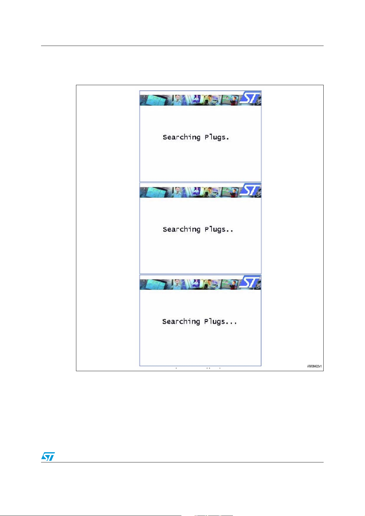
Figure 15. Searching plugs . . . . . . . . . . . . . . . . . . . . . . . . . . . . . . . . . . . . . . . . . . . . . . . . . . . . . . . . . 39
Figure 16. No plug detected. . . . . . . . . . . . . . . . . . . . . . . . . . . . . . . . . . . . . . . . . . . . . . . . . . . . . . . . . 40
Figure 17. Plugs detected . . . . . . . . . . . . . . . . . . . . . . . . . . . . . . . . . . . . . . . . . . . . . . . . . . . . . . . . . . 40
Figure 18. Label changing . . . . . . . . . . . . . . . . . . . . . . . . . . . . . . . . . . . . . . . . . . . . . . . . . . . . . . . . . . 41
Figure 19. TRIAC smartplug management . . . . . . . . . . . . . . . . . . . . . . . . . . . . . . . . . . . . . . . . . . . . . 41
Figure 20. Relay smartplug management . . . . . . . . . . . . . . . . . . . . . . . . . . . . . . . . . . . . . . . . . . . . . . 42
Figure 21. Smartplug statistics. . . . . . . . . . . . . . . . . . . . . . . . . . . . . . . . . . . . . . . . . . . . . . . . . . . . . . . 42
Figure 22. Energy consumption . . . . . . . . . . . . . . . . . . . . . . . . . . . . . . . . . . . . . . . . . . . . . . . . . . . . . . 43
Figure 23. Global energy consumption . . . . . . . . . . . . . . . . . . . . . . . . . . . . . . . . . . . . . . . . . . . . . . . . 43
Figure 24. Power consumption . . . . . . . . . . . . . . . . . . . . . . . . . . . . . . . . . . . . . . . . . . . . . . . . . . . . . . 44
Figure 25. Global power consumption . . . . . . . . . . . . . . . . . . . . . . . . . . . . . . . . . . . . . . . . . . . . . . . . . 44
Figure 26. ZigBee and dual interface EEPROM adapter schematic for STM3210C-EVAL . . . . . . . . . 45
Figure 27. ZigBee and dual interface EEPROM adapter layout for STM3210C-EVAL . . . . . . . . . . . . 46
Figure 28. STM3210C main schematic . . . . . . . . . . . . . . . . . . . . . . . . . . . . . . . . . . . . . . . . . . . . . . . . 47
Figure 29. MCU schematic . . . . . . . . . . . . . . . . . . . . . . . . . . . . . . . . . . . . . . . . . . . . . . . . . . . . . . . . . 48
Figure 30. LCD schematic . . . . . . . . . . . . . . . . . . . . . . . . . . . . . . . . . . . . . . . . . . . . . . . . . . . . . . . . . . 49
Figure 31. I/O expander schematic . . . . . . . . . . . . . . . . . . . . . . . . . . . . . . . . . . . . . . . . . . . . . . . . . . . 50
Figure 32. I/O peripherals . . . . . . . . . . . . . . . . . . . . . . . . . . . . . . . . . . . . . . . . . . . . . . . . . . . . . . . . . . 51
Figure 33. Extension connector . . . . . . . . . . . . . . . . . . . . . . . . . . . . . . . . . . . . . . . . . . . . . . . . . . . . . . 52
Figure 34. JTAG and trace. . . . . . . . . . . . . . . . . . . . . . . . . . . . . . . . . . . . . . . . . . . . . . . . . . . . . . . . . . 53
Figure 35. Power . . . . . . . . . . . . . . . . . . . . . . . . . . . . . . . . . . . . . . . . . . . . . . . . . . . . . . . . . . . . . . . . . 54
Figure 36. LCD 3.2" module with SPI and 16-bit interface 1 . . . . . . . . . . . . . . . . . . . . . . . . . . . . . . . . 55
Doc ID 18209 Rev 1 5/58

Document and library rules AN3311
1 Document and library rules
This document uses the conventions described in the sections below.
1.1 Acronyms
Ta bl e 1 lists the acronyms used in this document.
Table 1. List of acronyms
Acronym Meaning
API Application programming interface
HAL Hardware abstraction layer
MCU Microcontroller unit
I2C Inter-integrated circuit
SPI Serial to parallel interface
OOP Object oriented programming
6/58 Doc ID 18209 Rev 1

AN3311 ZigBee smartplug
2 ZigBee smartplug
2.1 Smartplug description
The smartplug coordinator is connected via an SPI to the STM3210C-EVAL through an “AdHoc” adapter.
In Figure 1 it is possible to take a quick look at the STM3210C-EVAL board and a smartplug
node block diagram.
Figure 1. STM3210C-EVAL block scheme
An adapter is connected to the extended connectors CN8 and CN9 on the STM3210CEVAL (for more detailed information please refer to the UM0600 user manual), it allows the
connection of a ZigBee smartplug coordinator and the I
2
C/RF dual interface EEPROM
M24LR64-r. The Gerber files of the adapter board are included in the setup package of this
project.
The ZigBee smartplug board can be used as a guide to build a home/building automation
subsystem for energy management. In a typical application, the board is plugged into an
electrical wall socket and supplies an electrical load, monitoring the energy consumption;
using several smartplugs it is possible to monitor and control the home/building energy
consumption socket by socket. The board includes the following functions, shown in the
block diagram of Figure 2:
● Energy measurement
● Load differential current
● Load driving by relay or TRIAC (dimming)
● ZigBee communication capability.
Doc ID 18209 Rev 1 7/58

ZigBee smartplug AN3311
Figure 2. Block diagram
The STEVAL-IHP001V3 is a smartplug board based on an STM32F10x microcontroller, a
SPZB260 ZigBee module, and an STPM01 energy metering IC.
It implements a ZigBee metering node which allows the final user to monitor and manage
energy consumption.
The board has been developed as a guide to build a home/building automation subsystem
for energy management. In a typical home system implementation, the board is plugged into
an electrical wall socket and supplies a home appliance or other generic electrical load.
The current, power, energy, and other information, related to the electrical load connected to
the smartplug board, can be displayed locally on an LCD screen, and are sent to a ZigBee
data concentrator through the home/building ZigBee network.
2.2 ZigBee module
ZigBee smartplug communication is based on the SPZB260 module with a DIL adapter. The
module is FCC compliant (FCC ID:S9NZB260A). The module is based on the SN260
ZigBee network processor which integrates a 2.4 GHz, IEEE 802.15.4 compliant
transceiver, as well as IEEE 802.15.4 PHY and MAC. The main features are:
● 0dBm nominal TX output power
● -92dBm RX sensitivity
● +2dBm TX output power in boost mode
● RX filtering for co-existence with IEEE 802.11g and Bluetooth
For further details please refer to the SPZB260 module and the SN260 network processor
datasheet.
Note: For more information, see the UM0608 user manual, STEVAL-IHP001V3 schematics
diagram, and AN2993 application note.
®
devices.
8/58 Doc ID 18209 Rev 1

AN3311 Multi-input embedded GUI library
3 Multi-input embedded GUI library
3.1 Description
This solution enables users, comfortable with the use of standard microcontrollers, to create
higher-end “look and feel” human interfaces by replacing conventional electromechanical
switches with touch-sensing controls.
Users can combine touch-sensing functions using multiple configurations (touchscreen,
joystick, and keys) with traditional MCU features (communication, beeper, LCD control, etc.).
The E-multi-input graphic library is part of the application firmware.
The graphic objects are a set of controls that can be printed on the screen and associated to
an action when pressed.
The library has been developed and tested on an LCD panel of QWGA resolution (320x240)
which is the default, but the library is independent of the LCD resolution, although it has not
been tested with others.
The library supports touchscreen features and includes a low level driver which handles the
analog input (for 12-bit ADC), and a function for the touchscreen calibration based on an
algorithm that uses 5 points.
The multi-input embedded GUI firmware library is fully developed in 'ANSI-C' following an
OOP approach. This means that the final application uses instances of page and graphic
objects according to their public methods and properties. In the end, the PageObj is a
structure containing public properties (data fields) and methods (functions pointers). The
OOP encapsulation feature is assured. The library has been developed and tested on the
“STM3210C” STMicroelectronics demonstration board.
The library can be included in the final application as a library file (multi-input embedded
GUI library.a) and used as a black box through its exported public API, or can be included in
the final application as source files (.c and .h), if the user wants to debug the library itself, or
to change the HAL functions in order to port the library on a different LCD (in model and
resolution) from the one attached to STM3210C-EVAL.
For more information on the graphic library see the AN3128, rev. 2, application note.
The calibration process is part of the post-processing layer. The touchscreen must be
calibrated at first power-on and/or upon user request.
Once the calibration is done, final adjustments on future power-on of the board are not
necessary because the calibration parameters are saved on the Flash memory.
The touchscreen and the joystick are controlled by the STMPE811 devices.
The STMPE811 has a simple 2-wire I
access the data in the touchscreen controller register at any time. It communicates via the
serial interface with a master controller.
Figure 3 shows how the STM32F10xxx microcontroller (master device) must be connected
to the STMPE811 device.
2
C digital serial interface which allows the user to
Refer to the STMPE811 datasheet for more information on the register concerning the data
of the touched points on the touchscreen.
Doc ID 18209 Rev 1 9/58

Multi-input embedded GUI library AN3311
Y-
1
INT
2
A0/Data
Out
3
4
5
VCC
6
Data in
7
IN0
8
IN1
9
GND
10
IN2
11
IN3
12
X+
13
Vio
14
Y+
15
X-
16
U7
STMPE81811
Y-
1
INT
2
A0/Data
Out
3
4
5
VCC
6
Data in
7
IN0
8
IN1
9
GND
10
IN2
11
IN3
12
X+
13
Vio
14
Y+
15
X-
16
U8
STMPE81811
R56
10K
+3V3
I2C
device
address:0x8 2
I2C
device
address:0x88
+3V3
+3V3
R57
100K
R58
100K
TouchScreen_X+
TouchScreen_X-
TouchScreen_Y+
TouchScreen_Y-
EXP_I_IO2
EXP_I_IO3
EXP_I_IO4
EXP_I_IO5
EXP_I_IO6
EXP_I_IO7
EXP_I_IO8
EXP_I_IO9
EXP_I_IO1O10
EXP_I_IO1O11
EXP_I_IO1O12
EXP_I_IO1
R160
10K
R159 0
+3V3
R37
10K
R164
10K
+3V3
C89
100nF
C90
100nF
PB6
PB7
P
B14
SCLK
SDAT
SCLK
SDAT
Figure 3. I/O expander hardware configuration on the STM3210C-EVAL
+3V
C8
100n
IO_Expander_SCK
IO_Expander_SDA
IO_Expander_INT
VC
14
Vio
10
GN
SCLK
B1
R15
+3V
R160
10
+3V
+3V
R3
10
C9
100n
R164
10
+3V
SDAT
Data
A0/Data
Out
ST
devic
address:0x8
VC
14
Vio
10
GN
SCLK
SDAT
Data
A0/Data
Out
R5
ST
10
devic
address:0x8
16
15
13
12
11
16
15
13
12
11
TouchScreen_Y-
TouchScreen_XTouchScreen_Y+
TouchScreen_X+
EXP
EXP
EXP
EXP
R5
100
EXP
EXP
EXP
EXP
EXP
EXP
EXP
EXP
R5
100
AM08449v1
10/58 Doc ID 18209 Rev 1

AN3311 STM3210C-EVAL demonstration board
4 STM3210C-EVAL demonstration board
Figure 4. STM3210C-EVAL demonstration board
Doc ID 18209 Rev 1 11/58

STM3210C-EVAL demonstration board AN3311
4.1 Features
● Three 5 V power supply options: power jack, USB connector, or daughterboard
● Boot from user Flash, system memory or SRAM
● I2S audio DAC, stereo audio jack
● 512 MByte (or bigger) micro-SD cardTM
● Both type A and B smartcard support
2
● I
C compatible serial interface 64-Kbit EEPROM, MEMS and I/O expander
● RS-232 communication
● IrDA transceiver
● USB-OTG full speed, USB mini-AB connector
● IEEE-802.3-2002 compliant Ethernet connector
● Two channels of CAN2.0A/B compliant connection
● Inductor motor control connector
● JTAG and trace debug support
● 3.2" 240x320 TFT color LCD with touchscreen
● Joystick with 4-direction control and selector
● Reset, wake-up, tamper, and user button
● 4 color LEDs
● RTC with backup battery
● MCU consumption measurement circuit
● Extension connector for daughterboard or wrapping board.
4.2 STM32 peripherals mapping
The STM3210C-EVAL demonstration board is designed around the STM32F107VC in a
100-pin TQFP package. The hardware block diagram, Figure 5, illustrates the connection
between the STM32F107VC and peripherals (LCD, EEPROM, MEMS, USART, IrDA, USBOTG, Ethernet, audio, CAN bus, smartcard, micro-SD card, and motor control) and these
features can be located on the actual demonstration board in Figure 6.
12/58 Doc ID 18209 Rev 1

AN3311 STM3210C-EVAL demonstration board
Figure 5. Hardware block diagram - STM32 peripherals mapping
6REGULATOR
-#5
CONSUMPTION
MEASUREMENT
,%$SKEY
%XTENSION
CONNECTORFOR
'0)/S
4&4,#$
-ICRO3$
CARD
-#CONTROL
CONNECTOR
*4!'
4RACE
".#CONNECTOR
0OTENTIOMETER
"ATTERYVOLTAGE
MEASUREMENT
'0)/
30)
-#
$EBUG
!$#
34-&6#4
)3
)#
/4'
-))2-)
#!.
#!.
53!24
53!24
!UDIO$!#
-%-3
%%02/-
)/EXPANDER
53"POWER
SWITCH
0(9
#!.
TRANSCEIVER
#!.
TRANSCEIVER
23
TRANSCEIVER
)R$!
TRANSCEIVER
3MARTCARD
INTERFACE
*OYSTICK
4OUCHSCREEN
53"-INI!"
CONNECTOR
)NTEGRATED2*
CONNECTOR
#!.
$"CONNECTOR
#!.
$"CONNECTOR
53!24
$"CONNECTOR
3MARTCARD
INTERFACE
!-V
For more details of calibration parameters, refer to the STPM01 datasheet on www.st.com.
Doc ID 18209 Rev 1 13/58

STM3210C-EVAL demonstration board AN3311
Figure 6. STM3210C-EVAL demonstration board layout
&1&1%1&
&1
&$1
&1
&$1
&1&1([WHQVLRQKHDGHU
8
)9&7
670
&10RWRUFRQWURO
&1
5-
FRQQHFWRU
&1
56
&1
86%0LFUR$%
FRQQHFWRU
&1
9SRZHU
&1
$XGLR MDFN
&1
0LFUR6'FDUG
&1
6PDUWFDUG
%
5HVHW
4.3 Power supply
The STM3210C-EVAL demonstration board is designed to be powered by a 5 V DC power
supply and protected by PolyZen from a wrong power plug-in event. It is possible to
configure the demonstration board to use any of the following three sources for the power
supply:
● 5 V DC power adapter connected to CN18, the power jack on the board (PSU on silk
screen for power supply unit)
● 5 V DC power with 500 mA limitation from CN2, the USB mini-AB connector (USB on
silkscreen)
● 5 V DC power from both CN8 and CN9, the extension connector for the daughterboard
(DTB for daughterboard on silkscreen).
%:DNHXS
%7DPSHU 8-R\VWLFN
&1
7U D F H
&1
-7$*
&1
&RORU/&'
8
,U'$
59
3RWHQW LR PHWH
%
8VHUNH\
U
!-V
14/58 Doc ID 18209 Rev 1

AN3311 STM3210C-EVAL demonstration board
The power supply is configured by setting the related jumpers JP24 and JP25, as described
in Ta bl e 2 .
Table 2. Power related jumpers
Jumper Description Configuration
JP25
selects one of the three possible power supply resources.
For power supply jack (CN18) to the STM3210C-EVAL only, JP25 is set as shown:
(Default)
For power supply from the daughterboard connectors (CN8 and CN9) to the
STM3210C-EVAL only, JP25 is set as shown:
JP25
For power supply from USB (CN2) to the STM3210C-EVAL only, JP25 is set as shown:
For power supply from power supply jack (CN18) to both the STM3210CEVAL
and daughterboard connected on CN8 and CN9, JP25 is set as
shown to the right (the daughterboard must not have its own power supply
connected):
bat is connected to 3.3 V power when JP24 is set as shown: (Default)
V
JP24
Vbat is connected to battery when JP24 is set as shown:
4.4 Boot option
The STM3210C-EVAL board is able to boot from:
● Embedded user Flash
● System memory with boot loader for ISP
● Embedded SRAM for debugging.
The boot option is configured by setting switches SW1 (BOOT1) and SW2 (BOOT0). The
BOOT0 can be configured also via the RS-232 connector CN6.
Doc ID 18209 Rev 1 15/58

STM3210C-EVAL demonstration board AN3311
Table 3. Boot related switches
Switch Boot from Configuration
STM3210C-EVAL boots from user Flash when SW2 is set as shown on
the right. SW1 setting does not matter in this configuration. (Default)
STM3210C-EVAL boots from system memory when SW1 and SW2 are
SW1 and SW2
set as shown:
STM3210C-EVAL boots from embedded SRAM when SW1 and SW2
are set as shown:
4.5 Clock source
Two clock sources are available on the STM3210C-EVAL demonstration board for
STM32F107VC, and RTC is embedded.
● X2, 32 kHz crystal for embedded RTC
● X3, 25 MHz crystal with socket for an STM32F107VC microcontroller, it can be
removed from the socket when an internal RC clock is used.
4.6 Reset source
The reset signal of the STM3210C-EVAL board is low active and the reset sources include:
● Reset button, B1
● Debugging tools from JTAG connector CN13 and trace connector CN12
● Daughterboard from CN9
● RS-232 connector CN6 for ISP.
Table 4. Reset related jumper
Jumper Description
JP20
Enables reset of the STM32F107VC embedded JTAG TAP controller each
time a system reset occurs. JP20 connects the TRST signal from the JTAG
connection with the system reset signal RESET#.
Default setting: not fitted.
16/58 Doc ID 18209 Rev 1

AN3311 STM3210C-EVAL demonstration board
4.7 Joystick
The joystick is four-directional and includes a selection key.
4.8 Pushbuttons
The following pushbuttons are provided:
● Key: user pushbutton
● Tamper: user pushbutton
● Wake-up: pushbutton used to wake up the processor from low-power mode.
4.9 Storage memory
The ZigBee adapter has a 64-Kbit I2C/RF dual interface memory (M24LR64-r) on board,
and it is connected to the I
2
The I
C address of the memory can be set by using the jumpers JP1 and JP2 on the ZigBee
adapter and must be different from the one already present on the STM3210C-EVAL (with
address 0xA0).
2
C1 peripheral of the MCU.
4.10 Development and debug support
The two debug connectors available on the STM3210C-EVAL demonstration board are:
1. CN13, standard 20-pin JTAG interface connector which is compliant with the debug
tools of ARM7 and ARM9
2. CN12, SAMTEC 20-pin connector FTSH-110-01-L-DV for both SWD and trace which is
compliant with ARM CoreSight
TM
debug tools
4.11 Display and input devices
The 3.2" TFT color LCD connected to SPI3 and 4 general purpose color LED's (LED 1, 2, 3,
4) are available as display devices.
A touchscreen connected to an I/O expander (U7), a 4-direction joystick with selection key, a
general purpose button (B3), a wake-up button (B2), and a tamper detection button (B4) are
available as input devices.
Table 5. LCD module
Pin on CN14 Description Pin connection
1 CS PB2
2RS-
3 WR/SCL PC10
4RD -
3.2" TFT LCD with touchscreen
CN14 (default)
Doc ID 18209 Rev 1 17/58

STM3210C-EVAL demonstration board AN3311
Table 5. LCD module (continued)
3.2" TFT LCD with touchscreen
CN14 (default)
Pin on CN14 Description Pin connection
5 RESET RESET#
22 BL_GND GND
23 BL_Control +5 V
24 VDD 3.3 V
25 VCI 3.3 V
26 GND GND
27 GND GND
28 BL_VDD +5 V
29 SDO PC11
30 SDI PC12
31 XL I/O Expander
32 XR I/O Expander
33 YD I/O Expander
34 YU I/O Expander
4.12 JTAG debugging connector CN13
Figure 7. JTAG debugging connector CN13 viewed from above the PCB
Table 6. JTAG debugging connector CN13
Pin number Description Pin number Description
1 3.3 V power 2 3.3 V power
3 PB4 4 GND
5PA156GND
7PA138GND
9PA1410GND
!-V
18/58 Doc ID 18209 Rev 1

AN3311 STM3210C-EVAL demonstration board
Table 6. JTAG debugging connector CN13 (continued)
Pin number Description Pin number Description
11 RTCK 12 GND
13 PB3 14 GND
15 RESET# 16 GND
17 DBGRQ 18 GND
19 DBGACK 20 GND
4.13 Daughterboard extension connector CN8 and CN9
Two 50-pin male headers, CN8 and CN9, can be used to connect a daughterboard or
standard wrapping board to the STM3210C-EVAL demonstration board. All 80 GPIOs are
available on it. The space between these two connectors and the power position, GND and
RESET pin are defined as a standard, which allows to develop common daughterboards for
several demonstration boards. The standard width between CN8 pin1 and CN9 pin1 is 2700
mills (68.58mm). This standard was implemented on the majority of demonstration boards.
Each pin on CN8 and CN9 can be used by a daughterboard after disconnecting it from the
corresponding function block on the STM3210C-EVAL demonstration board.
Table 7. Daughterboard extension connector CN8
Pin Description Alternate function
1GND -
3PC7 MC
5 PC9 USB power switch On Remove R36
7 PA9 USB VBUS Remove R78
9 PA0 MC/Ethernet/WKUP
11 PC14 via SB1 32 kHz oscillator Remove R161, close SB1
13 PA12 USB_DP Remove R43 or disconnect USB cable
15 PC15 via SB2 32 kHz oscillator Remove R59, close SB2
17 PC10 SPI1_CLK
19 GND -
21 PC12 SPI1_MOSI
23 PD1 CAN1_TX
25 PD3 LD3 Remove R96
How to disconnect with function block on STM3210C-
EVAL board
Disconnect STM3210C-EVAL board from motor power drive
board
Keep JP14 open. Disconnect STM3210C-EVAL board from
motor power drive board.
27 PD5 USART2_TX
29 PD7 LD1 Remove R94
31
Doc ID 18209 Rev 1 19/58

STM3210C-EVAL demonstration board AN3311
Table 7. Daughterboard extension connector CN8 (continued)
Pin Description Alternate function
33 PB3 TDO/SWO
35 PB5 CAN2_RX Remove R45
37 PB7 I2C1_SDA Remove R132
39 GND -
41 PE2 Trace_CK
43 PE4 Trace_D1
45 PB8 MC
47 PE6 Trace_D3
49 D5V
2 PC6 I2S_MCK/MC JP10 open
4PC8 MC
6 PA8 MCO JP4 open
8 PA10 USB_ID Remove R38 or disconnect USB cable
10 GND
12 PA11 USB_DM Remove R42 or disconnect USB cable
How to disconnect with function block on STM3210C-
EVAL board
Disconnect STM3210C-EVAL board from motor power drive
board
Disconnect STM3210C-EVAL board from motor power drive
board
14 PA13 TMS/SWDIO
16 PA14 TCK/SWCLK
18 PC11 SPI1_MISO Remove R135 and LCD
20 PA15 TDI
22 PD0 CAN1_RX Remove R44
24 PD2 MC
26 PD4 LD4 Remove R97
28 PD6 USART2_RX Keep JP16 open
30 GND
32
34 PB4 TRST Keep JP20 open
36 PB6
38 PE0
40 PE1 USB_Overcurrent Remove R35
42 PE3 Trace_D0
44 PE5 Trace_D2
CAN2_TX/
I2C1_SCK
MC/Micro-SD card
detection
Disconnect STM3210C-EVAL board from motor power drive
board.
Keep JP9 open
Remove micro-SD card. Disconnect STM3210C-EVAL board
from motor power drive board.
20/58 Doc ID 18209 Rev 1

AN3311 STM3210C-EVAL demonstration board
Table 7. Daughterboard extension connector CN8 (continued)
Pin Description Alternate function
46 PB9 User button Remove R104
48 3.3 V
50 GND
How to disconnect with function block on STM3210C-
EVAL board
Table 8. Daughterboard extension connector CN9
Pin Description Alternate function
1GND -
3 PD14 MC
5 PD12 Ethernet Remove RS2
7 PD10 Ethernet/smartcard Keep JP11 open
9
11 RESET# -
13 PB15 I2S_DIN
PC13 button
B3
IDD_CNT_EN /
Anti-tamper button
B4
How to disconnect with function block on STM3210C-
EVAL board
Keep JP22 open. Disconnect STM3210C-EVAL board from
motor
power drive board.
Keep JP1 open
15 PB13 I2S_CK/Ethernet Remove RS3
17 PB11 Ethernet Remove RS3
19 D5V -
21 PE14 Smartcard_CMDVCC Remove R166
23
25 PE12 MC
27 PE10 MC
29 PE8 MC
31 PE7 Smartcard_OFF Remove R69
33 PB1 MC Remove R168
35 PC5 VBAT_voltage Remove R154
37 PA7 MC Remove R169
39 GND
41 PA4
43 PA2 Ethernet Remove R162
45 PC3 Ethernet Remove RS1
Micro-SD card/
Audio_DAC
Disconnect STM3210C-EVAL board from motor power drive
board
Keep JP15 open
Doc ID 18209 Rev 1 21/58

STM3210C-EVAL demonstration board AN3311
Table 8. Daughterboard extension connector CN9 (continued)
Pin Description Alternate function
47 PC1 Ethernet
IDD_CNT_EN /
49 PC13
2PD15 MC
4 PD13 LD2 Remove R95
6 PD11 Ethernet Remove RS1
8 PD9 Ethernet/smartcard Keep JP12 open
10 GND
12 PD8 Ethernet/smartcard Keep JP13 open
14 PB14 IO_Expander_INT Remove R159
16 PB12 Ethernet/audio Remove RS3
18 PB10 Ethernet Remove RS2
20 PE15 MC Remove R139
22 PE13 MC
24
26 PE11 MC
28 PE9 MC
30 GND
Anti-tamper button
B4
How to disconnect with function block on STM3210C-
EVAL board
Keep JP1 open
Disconnect STM3210C-EVAL board from motor power drive
board
Disconnect STM3210C-EVAL board from motor power drive
board
Disconnect STM3210C-EVAL board from motor power drive
board
32 PB2 MC Remove R168
34 PB0 MC Remove R167
36 PC4 Potentiometer Remove R103
38 PA6 IDD_Measurement Remove R79
40 PA5 MC Remove R84
42 PA3 MC/Ethernet Keep JP10 open
44 PA1 Ethernet Keep JP3 open
46 PC2 Ethernet Remove RS1
48 PC0 MC/smartcard Remove R165
50 GND
22/58 Doc ID 18209 Rev 1

AN3311 STM3210C-EVAL demonstration board
4.14 TFT LCD connector CN14
One 34-pin male header CN14 is available on the board to connect LCD module board
MB785.
4.15 Power connector CN18
The STM3210C-EVAL demonstration board can be powered from a DC 5 V power supply
via the external power supply jack (CN18) shown in Figure 8. The central pin of CN18 must
be positive.
Figure 8. Power supply connector CN18 viewed from the front
'&9
*1'
For more information on STM3210C-EVAL, please refer to the UM0600 user manual.
!-V
Doc ID 18209 Rev 1 23/58

Demonstration firmware system setup AN3311
5 Demonstration firmware system setup
5.1 Hardware requirements
a) ZigBee adapter board
b) ZigBee module SPZB260-PRO
c) VDC/2A isolated power supply is recommended
d) One JTAG programmer/debugger dongle (J-Link from SEGGER or IAR Systems™
is recommended). It is unnecessary if no modifications to the firmware code have
been performed.
5.2 STM3210C-EVAL demonstration board setup
Set up the STM3210C-EVAL board as follows:
● Close jumper JP19
● Keep JP15 open
● Remove R79, R84, and R169.
5.3 STM3210C-EVAL and ZigBee adapter with M24LR62-r memory
Table 9. ZigBee adapter pin description
STM32 pin no. Pin name
- VDD 3.3 V CN8 - Pin 48 VCC_3V3
- VSS GND CN9 - Pin 50 GND
29 PA4 SPI1_NSS CN9 - Pin 41 ZIG_SS
30 PA5 SPI1_CLK CN9 - Pin 40 ZIG_SCLK
31 PA6 SPI1_MISO CN9 - Pin 38 ZIG_MISO
32 PA7 SPI1_MOSI CN9 - Pin 37 ZIG_MOSI
92 PB6 CAN2_TX/I2C1_SCK CN8 - Pin 36 I2C1_SCK
93 PB7 I2C1_SDA CN8 - Pin 37 I2C1_SDA
2 PE3 Trace_D0 CN8 - Pin 42 ZIG_HOST_INT
3 PE4 Trace_D1 CN8 - Pin 43
4 PE5 Trace_D2 CN8 - Pin 44 ZIG_WAKE
5 PE6 Trace_D3 CN8 - Pin 47 ZIG_RSTB
STM3210C-EVAL I/O
assignment
Extension connector pin
no.
ZigBee adapter I/O
assignment
VCC-GPIO (for M24LR64-
r)
24/58 Doc ID 18209 Rev 1

AN3311 Demonstration firmware system setup
5.4 How to navigate the demo menu
Four basic elements constitute the hardware of the system user interface: a 320 x 240 TFT
LCD display, a resistive touchscreen, a 5-way (left, right, up, down, selection) micro-joystick
and a pushbutton “Key”.
The joystick is primarily used for navigating between the various menu screens, within a
screen and between screen items. In addition, the joystick allows the selection and editing of
item values.
Doc ID 18209 Rev 1 25/58
In-home display firmware AN3311
p
{
ZigB
k
R
u
r
{
t
{
{
t
d
e
{
6 In-home display firmware
6.1 Firmware architecture
Figure 9. In-home display firmware architecture
InHome Display Firmware Architecture
on
F
r
e
e
T
O
S
licati
Ap
t
i-Inp
Mul
SmartPlug Coordinator
Layer
y
Multi-Input GUI Layer
Libra
GUI
LCD HAL
ee Stac
SPI
ZigBee Adapter and RF
Antenna for I2C Dual
Interface Memory
SPI
ware
nden
Har
Dep
This section describes the firmware implementation. The tasks/functions are described in
the following format:
Table 10. Function description format
Function name The name of the function
Function prototype Prototype declaration of the function
Behavior description Brief explanation of how the function is executed
Input parameter {x} Description of the input parameters
Output parameter {x} Description of the output parameters
Return value Value returned by the function
Required preconditions Requirements before calling the function
Called functions Other library functions called
LCD Libraries
STM32F10xx Libraries
I2C
AM08462v1
26/58 Doc ID 18209 Rev 1
AN3311 In-home display firmware
6.2 main.c
6.2.1 vSmartPlugSamplingTask
Ta bl e 1 1 describes the vSmartPlugSamplingTask task:
Table 11. vSmartPlugSamplingTask task
Function name vSmartPlugSamplingTask
Function prototype void vSmartPlugSamplingTask(void *pvParameters)
Behavior description Read and sample the plug consumption values
Input parameter {x} None
Output parameter {x} None
Return value None
Required preconditions None
Called functions No API/HAL layer functions;
Example:
static void vSmartPlugSamplingTask( void *pvParameters)
{
CoordinatorType* pObjCoordinator = GetCoordinatorObj();
int i=0;
sinkAdvertise();
pObjCoordinator = GetCoordinatorObj();
//Get the Smart-Plug list
ppSmartPlugList = pObjCoordinator->GetSmartPlugList(pObjCoordinator);
while(1)
{
if ( ppSmartPlugList[0] )
{
smart_points1[i%N_SAMPLES] = ppSmartPlugList[0]->Energy;
smart_points1B[i%N_SAMPLES] = ppSmartPlugList[0]->Power;
}
if ( ppSmartPlugList[1] )
{
smart_points2[i%N_SAMPLES] = ppSmartPlugList[1]->Energy;
smart_points2B[i%N_SAMPLES] = ppSmartPlugList[1]->Power;
}
i++;
if(i == N_SAMPLES)
{
i=0;
for(int j=0; j<N_SAMPLES; j++)
{
smart_points1[j] = 0;
smart_points1B[j] = 0;
smart_points2[j] = 0;
smart_points2B[j] = 0;
}
}
if( i%8 == 0 )
Doc ID 18209 Rev 1 27/58

In-home display firmware AN3311
sinkAdvertise();
vTaskDelay(2000); //20 sec
}
}
The application simulates the behavior of the system in a 24 hour period considering an
hour as equal to 20 seconds. After 24 hours (simulated), it resets the array values, so the
GraphCharts and the histograms show a maximum value set to zero.
6.2.2 vGraphicLibraryTask
Ta bl e 1 2 describes the vGraphicLibraryTask task:
Table 12. vGraphicLibraryTask task
Function name vGraphicLibraryTask
Function prototype void vGraphicLibraryTask(void *pvParameters)
Behavior description
Input parameter {x} None
Output parameter {x} None
Check if an input device has been stimulated (touchscreen or
joystick/button)
Return value None
Required preconditions None
Called functions No API/HAL layer functions;
This function checks if an input device has been stimulated (touchscreen or joystick/button)
and calls the graphic library relative function according to the object pressed.
Example:
static void vGraphicLibraryTask( void *pvParameters )
{
/* Menu Initialization*/
MENU_DeInit();
CursorShow(195, 50);
/* Infinite main loop ------------------------------------------------------*/
while (1)
{
ProcessTouchScreenData();
/*Time out calculate for power saving mode*/
TimeOutCalculate();
#ifdef USE_STM3210C_EVAL
if (restart_calibration==1)
{
TS_Calibration();
restart_calibration = 0;
MENU_DeInit();
}
CursorReadJoystick(IOEXP_MODE);
TSC_Read();
#else
28/58 Doc ID 18209 Rev 1
AN3311 In-home display firmware
CursorReadJoystick(POLLING_MODE);
#endif
vTaskDelay(2);
}
}
6.2.3 prvApplicationTask
Ta bl e 1 3 describes the prvApplicationTask task:
Table 13. prvApplicationTask task
Function name prvApplicationTask
Function prototype void prvApplicationTask (void *pvParameters)
Behavior description Start the Smartplug Coordinator Application routine
Input parameter {x} None
Output parameter {x} None
Return value None
Required preconditions None
Called functions No API/HAL layer functions;
This function starts the smartplug coordinator application routine.
Example:
void prvApplicationTask( void * pvParameters )
{
/* The parameters are not used in this task. */
( void ) pvParameters;
for( ;; )
{
applicationTick();
/* Wait until it is time to move onto the next string. */
vTaskDelay(4);
}
}
6.2.4 prvSetupHardware
Ta bl e 1 4 describes the prvSetupHardware function:
Table 14. prvSetupHardware function
Function name prvSetupHardware
Function prototype void prvSetupHardware (void)
Behavior description
Input parameter {x} None
Output parameter {x} None
Initialize the hardware peripheral of the STM32 MCU, and ZigBee
hardware configuration
Return value None
Doc ID 18209 Rev 1 29/58
In-home display firmware AN3311
Table 14. prvSetupHardware function (continued)
Required preconditions None
Called functions No API/HAL layer functions;
This function is intended to initialize the hardware peripherals of the STM32 MCU, and the
ZigBee hardware configuration.
Example:
static void prvSetupHardware( void )
{
SystemInit();
/* Enable GPIOA, GPIOB, GPIOC, GPIOD, GPIOE and AFIO clocks */
RCC_APB2PeriphClockCmd(RCC_APB2Periph_GPIOA | RCC_APB2Periph_GPIOB |
RCC_APB2Periph_GPIOC | RCC_APB2Periph_GPIOD |
RCC_APB2Periph_GPIOE | RCC_APB2Periph_AFIO, ENABLE );
/* Set the Vector Table base address at 0x08000000 */
NVIC_SetVectorTable( NVIC_VectTab_FLASH, 0x0 );
NVIC_PriorityGroupConfig( NVIC_PriorityGroup_4 );
/* Configure HCLK clock as SysTick clock source. */
SysTick_CLKSourceConfig( SysTick_CLKSource_HCLK );
/* Initialize the board */
vBoardInit();
EZSP_Init(); //init OBJ Coordinator
}
6.2.5 vBoardInit
Ta bl e 1 5 describes the vBoardInit function:
Table 15. vBoardInit function
Function name vBoardInit
Function prototype void vBoardInit (void)
Behavior description Initialize the hardware peripheral of the STM3210C-EVAL board
Input parameter {x} None
Output parameter {x} None
Return value None
Required preconditions None
Called functions No API/HAL layer functions;
This function is intended to initialize the hardware peripheral of the STM3210C-EVAL board
and the graphic library hardware parameters.
Regarding the file menu.c, it just uses the API function of the graphic library and some
others of the “ZigBee stack for smartplug”, for more information please refer to the AN3128,
rev. 2, application note.
30/58 Doc ID 18209 Rev 1

AN3311 Getting started with the system
7 Getting started with the system
7.1 Configure IAR tool for building, debugging, and programming the application
Together with the firmware library package, an example application is delivered in order to
provide the final user with a real example of “In-home display” application usage.
The delivered example application has been written and developed using IAR EWARM 5.40
IDE and can be built for both STM32F10xxx medium-density and high-density
microcontroller families.
The workspace is created using the IAR embedded Workbench 5.40 IDE, using the ARM
based 32-bit STM32F10xx firmware library (ver. 3.1.2) CMSIS compliant, and in C
language.
The tree structure of the project is organized separating and grouping the source files with
the header files, both for the project files and the library files, as shown in Figure 10.
Figure 10. Application project files
®
-
In order to load the project, click on File\Open\Workspace and in the window that appears
select, in \project folder\EWARM, the file “Project.eww”.
Doc ID 18209 Rev 1 31/58

Getting started with the system AN3311
Figure 11. IAR embedded workbench main window
On the main node, where the program name located in the files window is shown, right click
the mouse button and select options. In the window which appears, select the debugger
item in the category list box, and select the proper debugging tool in the driver list box, then
press the Ok button. In the proposed example the J-Link dongle is used (Figure 12).
Press the Make icon or click on Project\Rebuild All. No error or warning should appear once
compiling has completed. Connect the J-Link tool to the USB port of the PC, and connect
the flat cable with the programming adapter. Plug the adapter into the dongle connector.
Press the debug icon, CTRL+D or click project\debug. The debugger starts to download the
firmware to the dongle through the J-Link debugger\programmer. Press the Go button, F5 or
click debug\go in order to execute the firmware in debug mode. To run the dongle in
standalone mode, press the stop debugging icon, CTRL+SHIFT+D or click debug\stop
debugging. Then remove the J-link adapter from the dongle and reset the board by
unplugging and plugging the power cable back in.
Figure 12. IAR embedded workbench debugger options
32/58 Doc ID 18209 Rev 1

AN3311 Getting started with the system
In order to use the In-home display application project, it is necessary to:
● Include all the firmware delivered in the In-home display package containing the
FreeRTOS core files. See Figure 10
● Create the desired menu application functions in the file menu.c
● Put inside “picture.c” the HEX dump of the pictures to be used with the application GUI
● Implement a main function as described in the following section.
7.2 Example application - main.c
An example of a main application is given below. The main function contains an example of
the In-home display application initialization/configuration and implements the classic
operations:
/* Standard includes. */
#include <stdio.h>
/* Scheduler includes. */
#include "FreeRTOS.h"
#include "task.h"
#include "queue.h"
#include "semphr.h"
/* Library includes. */
#include "stm32f10x.h"
#include "stm32f10x_it.h"
#include "STM3210c_eval_lcd.h"
#include "LcdHal.h" //SB
/* Demo app includes. */
#include "flash.h"
#include "partest.h"
#include "common.h"
#include "micro_clocks_irqs.h"
#include "micro.h"
#include "menu.h"
#include "graphicObject.h"
#include "cursor.h"
#include "stm32d-eval_io_expander.h"
#include "LcdHal.h"
#include "TscHal.h"
#include "pictures.h"
#include "stm32f10x.h"
#include "stm32f10x_rcc.h"
#include "misc.h"
#include "SmartPlugObj.h"
#include "CoordinatorObj.h"
#include "COORDINATOR_Layer.h"
#include "ZSP_Layer.h"
#ifdef USE_STM3210E_EVAL
#include "stm3210e_eval_lcd.h"
#elif USE_STM3210C_EVAL
#include "stm3210c_eval_lcd.h"
#include "touchscreen.h"
#endif
/* Private define ------------------------------------------------------------*/
Doc ID 18209 Rev 1 33/58

Getting started with the system AN3311
/* Touchscreen Controller and Joystick DEFINES */
#define TSC_GPIO_PORT_SOURCE GPIO_PortSourceGPIOB
#define TSC_GPIO_PIN_SOURCE GPIO_PinSource14
#define JOY_GPIO_PORT_SOURCE GPIO_PortSourceGPIOB
#define JOY_GPIO_PIN_SOURCE GPIO_PinSource14
#define JOY_GPIO_SELECT_PORT GPIOG
#define JOY_GPIO_SELECT_PIN GPIO_Pin_7
#define JOY_GPIO_RIGHT_PORT GPIOG
#define JOY_GPIO_RIGHT_PIN GPIO_Pin_13
#define JOY_GPIO_LEFT_PORT GPIOG
#define JOY_GPIO_LEFT_PIN GPIO_Pin_14
#define JOY_GPIO_UP_PORT GPIOG
#define JOY_GPIO_UP_PIN GPIO_Pin_15
#define JOY_GPIO_DOWN_PORT GPIOD
#define JOY_GPIO_DOWN_PIN GPIO_Pin_3
#define JOY_GPIO_RCC_APB_PERIPH1 RCC_APB2Periph_GPIOG
#define JOY_GPIO_RCC_APB_PERIPH2 RCC_APB2Periph_GPIOG
#define JOY_GPIO_RCC_APB_PERIPH3 RCC_APB2Periph_GPIOG
#define JOY_GPIO_RCC_APB_PERIPH4 RCC_APB2Periph_GPIOG
#define JOY_GPIO_RCC_APB_PERIPH5 RCC_APB2Periph_GPIOD
#define TSC_EXTI_IRQ_CHANNEL EXTI15_10_IRQn
#define JOY_EXTI_IRQ_CHANNEL EXTI15_10_IRQn
#define TSC_EXTI_LINE EXTI_Line14
#define JOY_EXTI_LINE EXTI_Line14
#define TSC_GPIO_PORT GPIOA
#define TSC_GPIO_PIN GPIO_Pin_14
#define TSC_I2C_DEVICE_REGISTER 0x82
#define JOY_I2C_DEVICE_REGISTER 0x88
#define M24LR64_I2C_DEVICE_REGISTER 0x24
#define TSC_I2C_PORT I2C1
/* User Button GPIO Port and Pin*/
#ifdef USE_STM3210C_EVAL
#define USER_BUTTON_PORT GPIOB
#define USER_BUTTON_PIN GPIO_Pin_9
#elif USE_STM3210E_EVAL
#define USER_BUTTON_PORT GPIOG
#define USER_BUTTON_PIN GPIO_Pin_8
#endif
/* LCD Controller DEFINES */
#define LCD_CTRL_PORT_NCS GPIOB
#define LCD_GPIO_DATA_PORT GPIOC
#define LCD_CTRL_PIN_NCS GPIO_Pin_2
#define LCD_CTRL_PIN_NWR GPIO_Pin_15
#define LCD_CTRL_PIN_RS GPIO_Pin_7
#define LCD_GPIO_PIN_SCK GPIO_Pin_10
#define LCD_GPIO_PIN_MISO GPIO_Pin_11
#define LCD_GPIO_PIN_MOSI GPIO_Pin_12
#define LCD_GPIO_RCC_APB_PERIPH RCC_APB2Periph_GPIOC
#define LCD_GPIO_RCC_APB_PERIPH_NCS RCC_APB2Periph_GPIOB
#define LCD_GPIO_REMAP_PORT GPIO_Remap_SPI3
#define LCD_RCC_APB_PERIPH RCC_APB1Periph_SPI3
#define LCD_RCC_AHB_PERIPH RCC_AHBPeriph_FSMC
#define LCD_SPI_PORT SPI3
#ifdef USE_STM3210C_EVAL
#define LCD_CONNECTION_MODE GL_SPI
#elif USE_STM3210E_EVAL
#define LCD_CONNECTION_MODE GL_FSMC
#endif
#define RCC_AHBPeriph_FSMC ((uint32_t)0x00000100)
34/58 Doc ID 18209 Rev 1

AN3311 Getting started with the system
/* Exported variables--------------------------------------------------------*/
LCD_HW_Parameters_TypeDef* pLcdParam;
TSC_HW_Parameters_TypeDef* pTscParam;
JOY_HW_Parameters_TypeDef* pJoyParam;
BTN_HW_Parameters_TypeDef* pBtnParam;
extern volatile GL_u8 touch_done;
GL_s16 smart_points1[N_SAMPLES];
GL_s16 smart_points1B[N_SAMPLES];
GL_s16 smart_points2[N_SAMPLES];
GL_s16 smart_points2B[N_SAMPLES];
SmartPlugType** ppSmartPlugList;
SmartPlugType* pCurrentSmartPlug;
extern GL_Page_TypeDef pageS2B;
extern GL_Page_TypeDef pageS2C;
/* Private macro -------------------------------------------------------------*/
/* Private variables ---------------------------------------------------------*/
static volatile ErrorStatus HSEStartUpStatus /*= SUCCESS*/;
volatile GL_u8 restart_calibration = 0;
GPIO_InitTypeDef GPIO_InitStructure;
static u32 TimingDelay;
static xTaskHandle xEmberTaskHandle, xApplTaskHandle, xSmartSamplingTaskHandle,
xGraphLibTaskHandle;
/* The time between cycles of the 'check' functionality (defined within the tick
hook. */
#define mainCHECK_DELAY ( ( portTickType ) 5000 / portTICK_RATE_MS )
/* Task priorities. */
#define EMBER_Task ( tskIDLE_PRIORITY + 3 )
#define APPLICATION_Tick_Task ( tskIDLE_PRIORITY + 2 )
#define mainINIT_TASK_PRIORITY ( tskIDLE_PRIORITY + 1 )
/* The period of the system clock in nano seconds. This is used to calculate the
jitter time in nano seconds. */
#define mainNS_PER_CLOCK ((unsigned portLONG)((1.0 /
(double)configCPU_CLOCK_HZ)*1000000000.0))
/*-----------------------------------------------------------*/
/* Configure the hardware for the demo. */
static void prvSetupHardware( void );
static void vEmberTickTask( void *pvParameters );
extern void EZSPInit(void);
static void prvApplicationTask( void * pvParameters );
void vApplication_EXIT2_ISRFunc( void );
void vApplication_USART0_ISRFunc( void );
/* Configure the hardware for the demo. */
static void prvSetupHardware( void );
/* Configure the board, LCD, Joystick, Button, GPIO and other peripherals as required
by the demo. */
static void vBoardInit( void );
/* Check Touchscreen, Joystick, Button in polling mode as required by the demo. */
static void vGraphicLibraryTask(void *pvParameters);
/* Check the SmartPlug Energy data as required by the demo. */
static void vSmartPlugSamplingTask( void *pvParameters);
Doc ID 18209 Rev 1 35/58

Getting started with the system AN3311
/*
* Configures the high frequency timers - those used to measure the timing
* jitter while the real time kernel is executing.
*/
extern void vSetupHighFrequencyTimer( void );
u16 ticksSinceLastHeard[APPLICATION_ADDRESS_TABLE_SIZE];
EmberNetworkStatus networkState = EMBER_NO_NETWORK;
/* insert Start */
xSemaphoreHandle xSemaphore_Ember = NULL;
xSemaphoreHandle xSemaphore_Serial = NULL;
extern void EZSP_Init(void);
extern void emberTick(void);
extern void processSerialInput(void);
extern void applicationTick(void);
/* insert End */
/*-------------------------*/
int main( void )
{
#ifdef DEBUG
debug();
#endif
pLcdParam = NewLcdHwParamObj ();
pTscParam = NewTscHwParamObj ();
pJoyParam = NewJoyHwParamObj ();
pBtnParam = NewBtnHwParamObj ();
prvSetupHardware();
/* Start the tasks. FreeRTOS API. */
xTaskCreate( vEmberTickTask, "EMBER", configMINIMAL_STACK_SIZE, NULL, EMBER_Task,
xEmberTaskHandle );
xTaskCreate( vSmartPlugSamplingTask, ( signed portCHAR * ) "SmartPlugSampling",
configMINIMAL_STACK_SIZE, NULL, tskIDLE_PRIORITY,
xSmartSamplingTaskHandle );
xTaskCreate( vGraphicLibraryTask, ( signed portCHAR * ) "GraphicLibrary",
configMINIMAL_STACK_SIZE*2, NULL, tskIDLE_PRIORITY+1,
xGraphLibTaskHandle );
/* Start the scheduler. */
vTaskStartScheduler();
// emberLeaveNetwork();
/* Will only get here if there was insufficient memory to create the idle task. The
idle task is created within vTaskStartScheduler(). */
for( ;; );
}
The initialization process is charged with preparing the basic mechanism of the system:
● Hardware peripheral configuration and initialization
● ZigBee stack initialization
● FreeRTOS task creation
● Starting system.
36/58 Doc ID 18209 Rev 1

AN3311 Getting started with the system
The clock distribution and the interrupt settings are two components that are strongly
dependent on the target project. An example of clock rate may be 72 MHz as the maximum
speed of the current STM32 microcontroller. It can be decreased to reduce the power
consumption. The clock rate assumptions are:
● System HCLK - 72 MHz
● Low speed peripheral PCLK1 - 72 MHz
● High speed peripheral PCLK2 - 36 MHz
● Analog to digital converter ADCCLK - 36 MHz
The interrupt setting situation is very similar to clock distribution. The library functions
involved with interrupt managing do not take the priorities into account; they only perform
very necessary and absolutely common settings to make them serviceable.
Doc ID 18209 Rev 1 37/58

In-home display GUI application AN3311
8 In-home display GUI application
If the ZigBee dongle is not connected or the resistors R79, R84, and R169 have not been
removed from the STM3210C-EVAL, the following screen is shown:
Figure 13. ZigBee dongle connection problem
After a board reset, if the firmware is correctly loaded into the Flash memory and the board
power is correctly supplied, the main screen is displayed as shown in Figure 14.
Figure 14. Main menu
38/58 Doc ID 18209 Rev 1
AN3311 In-home display GUI application
If Search Plugs is selected, the coordinator scans for smartplug devices for a certain length
of time and the display shows the following screens in loop:
Figure 15. Searching plugs
After that, if some plugs are connected, it adds them to the smartplug list and then shows
the home screen.
Doc ID 18209 Rev 1 39/58

In-home display GUI application AN3311
If you click on Management two situations are possible:
● If no plug is connected to the smartplug coordinator, the following screen is shown:
Figure 16. No plug detected
● Once more plugs are detected, the following screen is shown:
Figure 17. Plugs detected
There are three main buttons: identify, modify, and control. They allow to manage the
smartplug device.
The Identify button is useful to activate the LED flashing on the relative plug, so this way the
user can easily identify which plug they are going to manage through the GUI.
If Modify is clicked, the user can change the label of the selected plug, through the screen
shown in Figure 18, choosing the new label from a list contained in a combobox.
40/58 Doc ID 18209 Rev 1

AN3311 In-home display GUI application
Figure 18. Label changing
The user should scroll the list of the labels and click on the Apply button in order to save the
information and set the label also in the plug device via ZigBee protocol.
When Control is clicked, it is possible to switch ON/OFF the smartplug, in case of relay type,
or regulate the output power, in case of TRIAC type. The following screens show both
possibilities:
Figure 19. TRIAC smartplug management
Doc ID 18209 Rev 1 41/58

In-home display GUI application AN3311
Figure 20. Relay smartplug management
In the home screen, by clicking on Statistics, it is possible to see the electrical consumption
of the single smartplug device or the total consumption related to all plugs connected to the
smartplug coordinator. The following screen is shown:
Figure 21. Smartplug statistics
42/58 Doc ID 18209 Rev 1
AN3311 In-home display GUI application
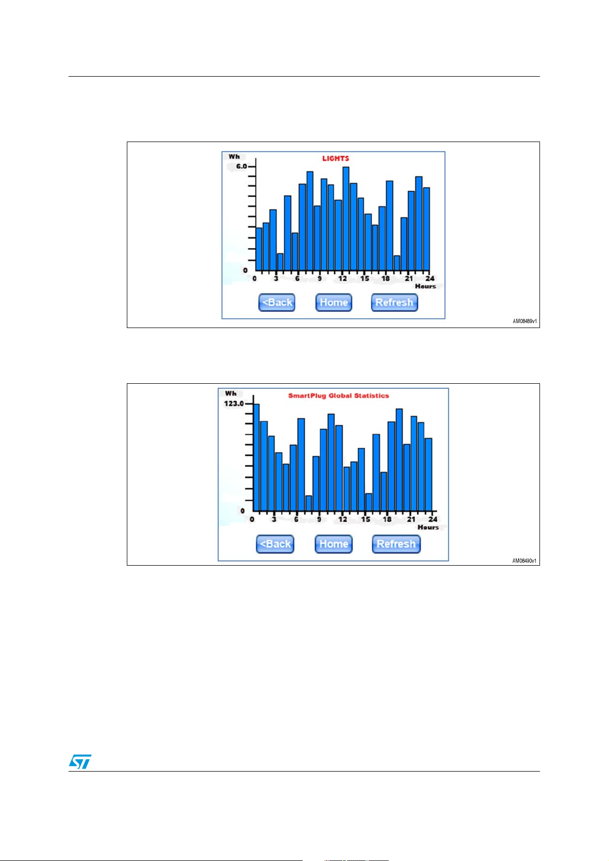
When Energy is clicked, the following screen, representing the energy consumption of the
selected smartplug device, is shown:
Figure 22. Energy consumption
When Global Energy is clicked, the following screen, representing the energy consumption
of the whole smartplug network, is shown:
Figure 23. Global energy consumption
Doc ID 18209 Rev 1 43/58

In-home display GUI application AN3311
When Power is clicked, the following screen, representing the power consumption of the
selected smartplug device, is shown:
Figure 24. Power consumption
When Global Power is clicked, the following screen, representing the power consumption of
the whole smartplug network, is shown:
Figure 25. Global power consumption
When the Refresh button is clicked, it is possible to make a refresh of the graph chart in
relation to the sampled points of the power consumption.
When the Home button is clicked, it returns to the home screen.
44/58 Doc ID 18209 Rev 1

AN3311 Schematics
9 Schematics
9.1 Smartplug board schematics and layout
Figure 26. ZigBee and dual interface EEPROM adapter schematic for STM3210C-EVAL
48R ev
o
meR -
)
KL
C_
1IPS(
5AP
PA6 (SPI1_MISO) - Remove R79
GND
ZIG_MISO
ZIG_SCLK
CN9
CN9
181920
10
8
14
5 6
1 2
3 4
9
7
111213
17
15 16
21 22
36
33 34
35
37 38
ZIG_MOSI
3940414243 44
9
6
SS_
1R
e
G
IZSS_GIZ
vo
meR - )IS
46
49 50
45
47 48
Header 25x2 (Female-Bottom)
Header 25x2 (Female-Bottom)
26
23 24
27 28
29 30
31 32
25
VCC_3V3
VCC_3V3
R3
4k7R34k7
2
Jumper
Jumper
1
R2
U1
3
GND
4k7R24k7
1
Jumper
Jumper
E1
VCC-GPIO
8
VCC
E01AC0
E0
JP2
JP2
3
JP1
JP1
2
I2C1_SDA
I2C1_SCK
5
7
6
E1
SCL
SDA
M24LR64U1M24LR64
VSS
AC1
3
2
4
GND
L1
4.7uHL14.7uH
SMD 7.8mm diameter, 5.3mm height
101112
CN8
CN8
1 2
3 4
5 6
7 8
9
13 14
O
M_1I
P
S( 7AP
PA4 (SPI1_NSS) - Keep JP15 open
ZIG_SCLK
ZIG_MOSI
ZIG_MISO
VCC_3V3
VCC_3V3
VCC_3V3
15 16
17 18
19 20
21 22
232425262728293031 32
MOSI
VBRDVBRD
1
23456
J2
J2
1
J4
J4
2
HOST_INT
ZIG_HOST_INT
R1
I2C1_SCK
36
33 34
35
MISO
SCLK
nSSEL
345
WAKE
RSTB
GND
ZIG_WAKE
ZIG_RSTB
4k7R14k7
PE3
42
39 40
37 38
41
I2C1_SDA
GND
6
GNDVCC-GPIO
VCC_3V3
3V3
PE5
444546
43
47 48
PE4
PE6
ZigBee - CONN1
ZigBee - CONN1
ZigBee - CONN2
ZigBee - CONN2
49 50
ZIGBEE/SPZB260-PRO
Header 25x2 (Female-Bottom)
Header 25x2 (Female-Bottom)
Prior to using this adapter, remove the required
resistance from the STM3210C-Eval Board
AM08515v1
Doc ID 18209 Rev 1 45/58

Schematics AN3311
9.2 ZigBee/RF adapter for smartplug and dual interface memory
Figure 27. ZigBee and dual interface EEPROM adapter layout for STM3210C-EVAL
46/58 Doc ID 18209 Rev 1

AN3311 Schematics
9.3 STM3210C
Figure 28. STM3210C main schematic
BNC1
MC_EmergencySTOP
MC_CurrentA
U_IO Peripherals
BNC2
JOY_SEL
LED4
LED3
LED1
LED2
IO Peripherals.SchDoc
JOY_LEFT
JOY_RIGHT
JOY_DOWN
EEPROM_SCK
EEPROM_SDA
MEMS_SCK
JOY_UP
MEMS_INT1
MEMS_INT2
Potentiometer
Anti_Tamper
MEMS_SDA
WAKEUP
User_Button
EXP_IO10
EXP_IO11
EXP_IO12
IO_Expander_SCK
IO_Expander_SDA
IO_Expander_INT
U_IO_Expander
IO_Expandor.SchDoc
R132 0
R131 0
EXP_IO9
R134
R133
EXP_IO1
TouchScreen_X-
TouchScreen_Y-
TouchScreen_X-
TouchScreen_Y-
TouchScreen_X+
TouchScreen_Y+
4K7
4K7
+3V3
U_LCD
LCD_CS
LCD.SchDoc
TouchScreen_X+
TouchScreen_Y+
LCD_CLK
LCD_DO
LCD_DI
RESET#
PA[0..15]
PB[0..15]
PC[0..15]
PD[0..15]
PE[0..15]
U_ExtensionConnector
RESET#
ExtensionConnector.SchDoc
USB_P owerSwitchOn
USB_DM
USB_DP
U_USB_OTG_FS
USB_OTG_FS.SchDoc
USB_OverCurrent
USB_VBUS
USB_ID
EXP_IO2
EXP_IO3
EXP_IO4
EXP_IO5
EXP_IO6
EXP_IO7
EXP_IO8
BNC1
BNC2
MC_PFCsync1
MC_PFCsync2
MC_WL
U_MotorControl
MotorControl.SchDoc
MC_VH
MC_VL
MC_UH
MC_UL
MC_WH
MC_NTC
MC_DissipativeBrake
MC_PFCpwm
MC_CurrentC
MC_EnA
MC_EnB
MC_HeatsinkTemperature
MC_BusVoltage
MC_EnIndex
MC_CurrentB
U_MCU
MCU.SchDoc
U_Audio
Audio.SchDoc
MC_VH
MC_WL
MC_PFCsync1
MC_PFCsync2
Audio_DAC_OUT
Audio_RST
Audio_SCK
Audio_SDA
Audio_DAC_OUT
MC_VL
I2S_CK
I2S_CK
MC_UH
I2S_DIN
I2S_DIN
MC_UL
MC_WH
I2S_CMD
I2S_MCK
I2S_MCK
I2S_CMD
MC_NTC
U_CAN
MC_EnB
MC_EnIndex
MC_PFCpwm
MC_BusVoltage
MC_DissipativeBrake
MC_HeatsinkTemperature
CAN1_TX
CAN1_RX
CAN2_TX
CAN2_RX
CAN1_TX
CAN2_TX
CAN1_RX
CAN2_RX
CAN.SchDoc
MC_EnA
MC_CurrentB
MC_CurrentC
MC_CurrentA
MC_EmergencySTOP
MicroSDCard_Detection
MicroSDCard_MISO
MicroSDCard_Detection
U_MicroSDCard
MicroSDCard.SchDoc
LED4
LED3
MicroSDCard_CS
MicroSDCard_CS
MicroSDCard_SCK
MicroSDCard_MOSI
U_JTAG&Trace
LED1
LED2
RESET#
TDI
TRST
TMS/SWDIO
TCK/SWCLK
TDI
TRST
RESET#
TMS/SWDIO
TCK/SWCLK
JTAG&Trace.SchDoc
WAKEUP
Anti_Tamper
Potentiometer
TRACE_D0
TRACE_CK
TDO/SWO
TDO/SWO
TRACE_D0
TRACE_CK
User_Button
TRACE_D3
TRACE_D2
TRACE_D1
TRACE_D3
TRACE_D2
TRACE_D1
I2C1_SCK
I2C1_SDA
IO_Expander_INT
MII_TX_CLK
MII_TX_CLK
U_Ethernet
Ethernet.SchDoc
IDD_Measurement
VBAT_Voltage_OUT
VBAT_Voltage
IDD_Measurement
Power.SchDoc
USB_ID
USB_DP
USB_DM
USB_P owerSwitchOn
IDD_CNT_EN
VBAT_DIV
LP_WAKEUP
IDD_CNT_EN
USB_VBUS
USB_VBUS
USB_OverCurrent
USART2_TX
USART2_RX
Bootloader_RESET
RS232/IrDA_TX
RS232/IrDA_RX
Bootloader_RESET
U_USART&IrDA
USART&IrDA.SchDoc
Bootloader_BOOT0
Bootloader_BOOT0
LCD_CS
SPI3_SCK
SPI3_MISO
SPI3_MOSI
MII_TX_EN
MII_RX_ER
MII_RX_DV/RMII_CRSDV
MII_COL
MII_CRS
MII_MDC
MII_TXD0
MII_TXD1
MII_TXD2
MII_TXD3
MII_RX_CLK/RMII_REF_CLK
MII_INT
MII_TXD0
MII_TXD1
MII_TXD2
MII_TXD3
MII_TX_EN
MII_RX_ER
MII_RX_DV/RMII_CRSDV
MII_RX_CLK/RMII_REF_CLK
MII_RXD0
MII_RXD0
MII_RXD1
MII_RXD1
MII_RXD2
MII_RXD2
MII_RXD3
MII_RXD3
MII_MDIO
MCO
MCO
MII_CRS
MII_COL
MII_MDC
MII_MDIO
PHY_RESET#
U_SmartCard
SmartCard.SchDoc
PB[0..15]
PC[0..15]
PA[0..15]
SmartCard_3/5V
SmartCard_IO
SmartCard_RST
SmartCard_CLK
SmartCard_CMDVCC
SmartCard_IO
SmartCard_RST
SmartCard_CLK
SmartCard_3/5V
SmartCard_CMDVCC
PE[0..15]
PD[0..15]
SmartCard_OFF
SmartCard_OFF
U_Power
AM08494v1
Doc ID 18209 Rev 1 47/58

Schematics AN3311
9.4 MCU
Figure 29. MCU schematic
PA[0..15]
PB[0..15]
PC[0..15]
PD[0..15]
PE[0..15]
PA[0..15]
PB[0..15]
PC[0..15]
PD[0..15]
PE[0..15]
MII_RX_DV/RMII_CRSDV
SmartCard_IO
SmartCard_RST
SmartCard_CLK
JP1
USB_P owerSwitchOn
SPI3_SCK
PC8
PC9
PC10
66
PC1078PC1179PC12
MC_EnA
I2S_MCK
321
MC_EnB
MC_EnIndex
VBAT_Voltage_OUT
PC5
PC6
PC7
34
PC663PC764PC865PC9
JP10
MII_TX_CLK
Potentiometer
PC2
PC3
PC4
18
PC433PC5
SmartCard_3/5V
MII_MDC
MII_TXD2
PC1
MC_HeatsinkTemperature
R165
0
MC_PFCpwm
LED2
MII_RXD2
MII_RXD3
PD11
PD12
PD13
PD14
PD15
PC0
62
PC015PC116PC217PC3
Anti_Tamper
IDD_CNT_EN
MC306-G-06Q-32.768 (manufacturer JFVNY)
R161
0
R59
0
321
SPI3_MISO
SPI3_MOSI
PC11
PC12
PC13
PC14
PC15
8
7
9
80
X2
C16
10pF
4 1
3 2
C17
10pF
MII_RXD0
MII_RXD1
321
321
JP12
USART2_TX
USART2_RX
LED4
PD3
PD4
PD5
LED3
PD2
321
MC_NTC
0DP51BP
PD1
JP13
CAN1_RX
MC_EmergencySTOP
PE15
46
PD081PD182PD283PD384PD485PD586PD687PD7
I2C device open / CAN2
==================================================
JP1: 2<->3 / Anti_Temper 1<->2 / MCU current measurement
JP9: close /
MC_WL
MC_WH
PE12
default set/ feature enabled another set/ feature enabled
MC_VH
MC_VL
PE10
PE11
PE1041PE1142PE1243PE1344PE1445PE15
PE9
40
MC_UH
MC_UL
PE8
JP10: 1<->2 / I2S Audio 2<->3 / MC
PE7
Jumper conguration:
SmartCard_CMDVCC
PE13
PE14
JP11
LED1
PD6
PD7
PD8
PD9
PD10
56
88
PD855PD9
PD1057PD1158PD1259PD1360PD1461PD15
1<->2 / Smartcard
/ Ethernet 2<->3 / WKUP & MC
JP11: 2<->3 / Ethernet
JP12: 2<->3 / Ethernet 1<->2 / Smartcard
JP13: 2<->3 / Ethernet 1<->2 / Smartcard
JP14: 1<->2
SmartCard_OFF
TRACE_D3
TRACE_D2
TRACE_D1
TRACE_D0
PE3
PE4
PE5
PE6
5
PE738PE839PE9
close / BL_Boot0
JP18: open/ BL_Boot0 disabled
JP19: open/ BL_Reset disabled close / BL_Reset
JP15: close / SDcard CS open / output for audio DAC
MC_PF Csync2
TRACE_CK
USB_OverCurrent
PE0
PE1
PE2
98
PE21PE32PE43PE54PE6
PE097PE1
JP26
U9A
TP6
MCO
321
WAKEUP
MII_CRS
MC_DissipativeBrake
PC14-OSC32_IN
PC15-OSC32_OUT
PC13-ANTI_TAMP
PA0-WKUP23PA124PA225PA326PA429PA530PA631PA7
PA0
PA1
PA2
PA3
PA4
PA5
MII_MDIO
MII_RX_CLK/RMII_REF_CLK
JP14
MII_COL
PA867PA968PA1069PA1170PA1271PA13
32
PA6
PA7
PA8
PA9
MCO
MC_CurrentA
MC_BusVoltage
IDD_Measurement
R78
USB_VBUS
JP15
MicroSDCard_CS
Audio_DAC_OUT
PA10
USB_ID
0
PA11
PA12
USB_DM
+3V3
72
PA13
PA14
USB_DP
TMS/SWDIO
2
SW1
1
PA1476PA15
77
PA15
PB0
TDI
TCK/SWCLK
R60 10K
09.03290.01
3
PB035PB136PB2
PB389PB490PB591PB692PB7
37
PB1
PB2
PB3
TDO/SWO
MC_CurrentB
MC_CurrentC MC_PF Csync1
LCD_CS
PB4
TRST
PB5
PB6
CAN2_RX
PB895PB9
93
PB7
PB8
I2C1_SDA
MII_TXD3
JP9
CAN2_TX
I2C1_SCK
PB1047PB1148PB1251PB1352PB1453PB15
96
PB9
PB10
PB11
PB12
User_Button
MII_TX_EN
MII_RX_ER
MII_TXD0
PB13
I2S_CMD
I2S_CK
54
PB14
IO_Expander_INT CAN1_TX
MII_TXD1
I2S_DIN
TP4
PTP_PPS
X3
25MHz (with socket)
OSC_IN12OSC_OUT13NRST
14
73
C18
20pF
NC
BOOT0
94
MicroSDCard_Detection
STM32F107VCT
Bootloader_BOOT0
+3V3
+3V3
C15
R62
D2
[N/A]
100nF
Bootloader_RESET
JP19
1N4148
RESET#
D1
1N4148
JP18
SW2
09.03290.01
20pF
3
2
1
2
B1
RESET
1
4 3
R61
10K
R63
220
C19
AM08495v1
48/58 Doc ID 18209 Rev 1

AN3311 Schematics
9.5 LCD
Figure 30. LCD schematic
LCD_DO
LCD_DI
LCD_CS
LCD_CLK
RESET#
PC11
PC12
PB2
PC10
+5V
+3V3
+5V
+3V3
+3V3
CN14
1
CS
2
RS
3
WR/SCL
4
RD
5
RESET
22
BL_GND
23
BL_Control
24
VDD
25
VCI
26
GND
27
GND
28
BL_VDD
29
SDO
30
SDI
3.2" LCD_connector (MB785 with AM-240320D4TOQW-T00H(R))
CN15
1
CS
2
SCL
3
SDI
4
RS
5
WR
6
RD
7
SDO
8
RESET
9
VDD
10
VCI
11
GND
12
GND
13
BL_VDD
14
BL_Control
15
BL_GND
16
BL_GND
2.4" LCD connector (MB542 with AM240320L8TNQW-00H)
PD1
PD2
PD3
PD4
PD5
PD6
PD7
PD8
PD10
PD11
PD12
PD13
PD14
PD15
PD16
PD17
6
7
8
9
10
11
12
13
14
15
16
17
18
19
20
21
31
XL
32
XR
33
YD
34
YU
To IO expandor
TouchScreen_X-
TouchScreen_X+
TouchScreen_Y-
TouchScreen_Y+
AM08496v1
Doc ID 18209 Rev 1 49/58

Schematics AN3311
9.6 I/O expander
Figure 31. I/O expander schematic
+3V3
C89
IO_Expander_SCK
IO_Expander_SDA
IO_Expander_INT
PB6
PB7
PB14
R159 0
+3V3
R160
10K
+3V3
+3V3
100nF
R37
10K
C90
100nF
R164
10K
+3V3
R56
10K
6
14
10
4
5
2
7
3
6
14
10
4
5
2
7
3
U7
VCC
Vio
GND
SCLK
SDAT
INT
Data in
A0/Data Out
STMPE811
I2C device address:0x82
U8
VCC
Vio
GND
SCLK
SDAT
INT
Data in
A0/Data Out
STMPE811
I2C device address:0x88
Y-
XY+
X+
IN3
IN2
IN1
IN0
Y-
XY+
X+
IN3
IN2
IN1
IN0
1
16
15
13
12
11
9
8
1
16
15
13
12
11
9
8
TouchScreen_Y-
TouchScreen_XTouchScreen_Y+
TouchScreen_X+
EXP_IO9
EXP_IO10
EXP_IO11
EXP_IO12
R57
100K
EXP_IO1
EXP_IO2
EXP_IO3
EXP_IO4
EXP_IO5
EXP_IO6
EXP_IO7
EXP_IO8
R58
100K
AM08497v1
50/58 Doc ID 18209 Rev 1

9.7 I/O peripherals
Figure 32. I/O peripherals
BNC1
BNC2
EEPROM
Doc ID 18209 Rev 1 51/58
U17
1
E0
2
E1
3
E2
VSS4SDA
M24C64-WMN6
PA7
PB0
BNC
VCC
WC
SCL
C91
100nF
8
7
6
5
PB6
PB7
CN10
VB334
4
5
+3V3
SB3
SB4
2
1
3
CN11
VB334
R107
10K
EEPROM_SCK
EEPROM_SDA
MEMS
MEMS_SDA
MEMS_SCK
MEMS_INT1
MEMS_INT2
To IO expander
R112 50
R113 50
2
345
JP17
AN3311 Schematics
U15
R108
5
COMMON
100
+3V3
10K
10K
R91
10K
10K
R90
R92
To IO expander
JOY_SEL
JOY_DOWN
JOY_LEFT
JOY_RIGHT
JOY_UP
1
LD1
Green
R94
C92
100nF
PB7
PB6
+3V3
1
6
3
13
14
8
9
LED1
LED2
LED3
LED4
U16
VDD_IO
VDD
Reserved
SDA
SCL
INT1
INT2
LIS302DL
SDO
GND
GND
GND
GND
Reserved
PD7
PD13
PD3
PD4
+3V3
R106
10K
7
CS
12
2
10
5
4
11
1 2
330
LD2
Orange
R95
1 2
680
LD3
Red
R96
1 2
680
LD4
Blue
R97
1 2
680
LEDs
Potentiometer
Potentiometer
R98 0
R99 0
R100 0
R101 0
R102 0
PC4
R89
C52 100nF
C53 100nF
C54 100nF
R103
0
C55 100nF
C60
10nF
R93
C56 100nF
10K
2
Selection
3
DWON
1
LEFT
4
RIGHT
6
UP
MT008-A
Joystick
R86
2 RV1
1K
+3V3
10K
1 3
User_Button
R104
0
R109
100
C59
[N/A]
+3V3
43
R117
220K
1
B2
WKUP
2
+3V3
R114
4K7
Anti_Tamper
2
3
B3
USER
1
4
C57
100nF
R110
100
+3V3
R115
R105
0
4K7
31CP9BP
Button
2
B4
Tamper
1
4 3
C58
100nF
WAKEUP
PA0
R116
330
R111
100
AM08516v1

Schematics AN3311
9.8 Extension connector
Figure 33. Extension connector
PC14
PC15
SB1
SB2
Open by default
Pin assignment niPdexif assignment xed
CN8
1 2
PC9
PA0
PC12
PD7
PB7
PE6
D5V
3 4
5 6
7 8
9 10
11 12
13 14
15 16
17 18
19 20
21 22
23 24
25 26
27 28
29 30
31 32
33 34
35 36
37 38
39 40
41 42
43 44
45 46
47 48
49 50
Header 25X2
PC6
PA8
PA14
PA15
PD0
PE0
PE1
8CP7CP
01AP9AP
PA11
31AP21AP
11CP01CP
2DP1DP
4DP3DP
6DP5DP
4BP3BP
6BP5BP
3EP2EP
5EP4EP
9BP8BP
+3V3
Pin assignment niPdexif assignment xed
thgiRtfeL
PC13
RESET#
D5V
PE8
PE7
PC13
CN9
1 2
3 4
5 6
7 8
R87
820
9 10
820
R88
11 12
13 14
15 16
17 18
19 20
21 22
23 24
25 26
27 28
29 30
31 32
33 34
35 36
37 38
39 40
41 42
43 44
45 46
47 48
49 50
Header 25X2
PD15
PD13PD14
PD11PD12
PD9PD10
PD8
PB14PB15
PB12PB13
PB10PB11
PE15
PE13PE14
PE11PE12
PE9PE10
PB2
PB0PB1
PC4PC5
PA6PA7
PA5
PA3PA4
PA1PA2
PC2PC3
PC0PC1
PA[0..15]
PB[0..15]
PC[0..15]
PD[0..15]
PE[0..15]
RESET#
AM08505v1
PA[0..15]
PB[0..15]
PC[0..15]
PD[0..15]
PE[0..15]
RESET#
52/58 Doc ID 18209 Rev 1
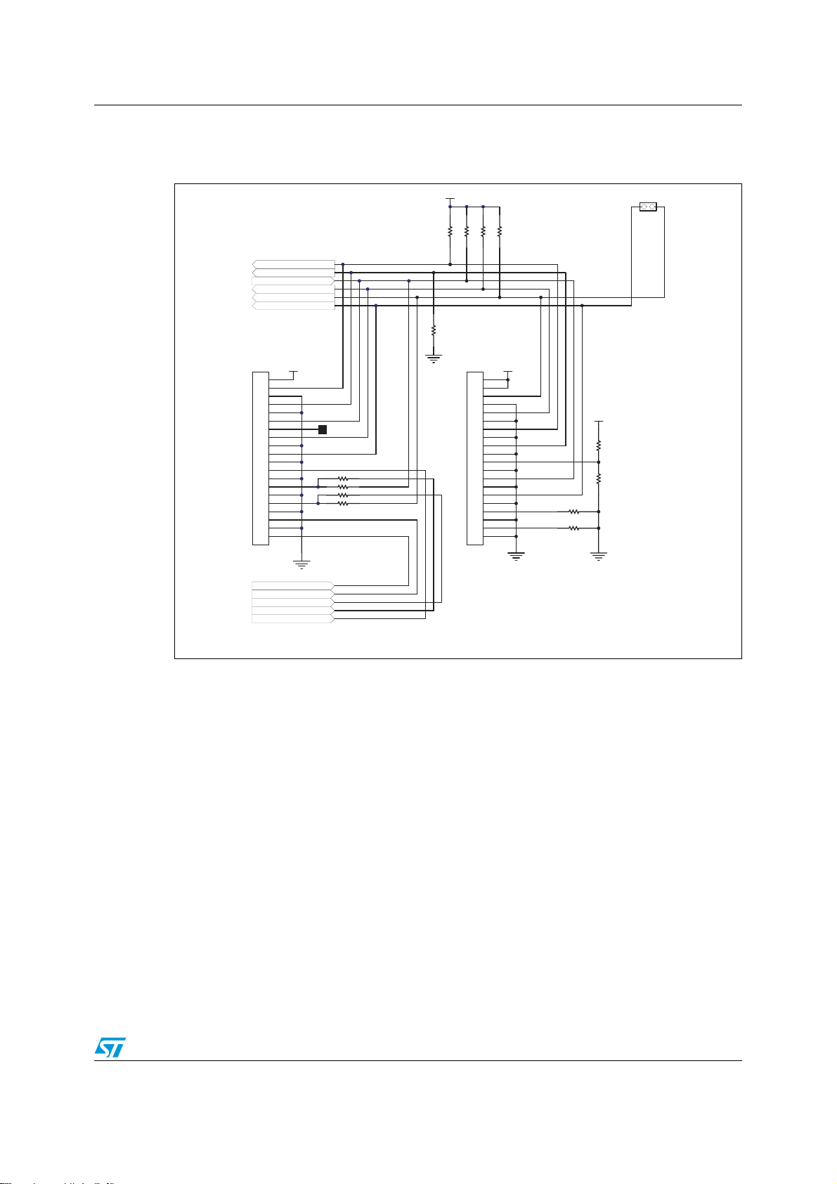
AN3311 Schematics
9.9 JTAG and trace
Figure 34. JTAG and trace
+3V3
R121
10K
R122
10K
R123
10K
R124
10K
JP20
TMS/SWDIO
TCK/SWCLK
TDO/SWO
TDI
TRST
RESET#
CN12
FTSH-110-01-L-DV
+3V3
1
2
3
4
5
6
7
8
9
10
11
12
13
14
15
16
17
18
19
20
TRACE_D3
TRACE_D2
TRACE_D1
TRACE_D0
TRACE_CK
KEY
R1290
R119[N/A]
R1300
R120[N/A]
Trace connector
PE6
PE5
PE4
PE3
PE2
PA13
PA14
PB3
PA15
PB4
R125
10K
CN13
JTAG
JTAG connector
+3V3
1
2
3
4
5
6
7
8
9
10
11
12
13
14
15
16
17
18
19
20
R127 10K
R128 10K
+3V3
R126
10K
R118
[N/A]
AM08506v1
Doc ID 18209 Rev 1 53/58

Schematics AN3311
9.10 Power
Figure 35. Power
TP12
Ground
+5V
TP11
BNX002-01
100nF
R147
0
49
74
19
VSSA
VSS_1
VSS_2
VDD_1
VDD_2
22
50
75
C87
C76
1uF
BEAD
99
VSS_3
VDD_3
100
100nF
TP10
27
VSS_4
VDD_4
28
5V
D5V E5V
3V3
U19
10
11
VSS_5
VDD_5
VDD_MCU
34
56
JP25
USB_VBUS 12
+3V3
C80
C75
2
Vout
GND
Vin
LD1086D2M33
3
C79_1
C79
+5V
VBAT
BARRACUDA_256K
6
100nF
10uF
1
220uF
220uF
VDD_MCU
R148
12
LD7
C85
C84
C83
C82
C81
321
1K5
TP5
100nF
100nF
100nF
100nF
100nF
red
2V5
+2V5
U27
LD1117S25TR
+5V
R150
10K(1%)
JP24
C51
2
Vout
Vin
3
VBAT_Voltage
PC5
R154
0
R151
BT1
CR1220 holder
10uF
1
R163
20K(1%)
VBAT_DIV
From IO expander
0
2
VDD_MCU
IDD_Measurement
PA6
R79
R149
2
O/I
I/O
U22
1
3
U21
MAX9938FEUK+
1
5
JP23
3
1
0
C78
4K7
4
4
+3V3
4
S
T1
0.47uF
+3V3
5
VCC
GND3C
R157 1K(1%)
R156
5
126
D
G
3
74H1G66STR
2
6
2
1
5
4
1(1%)
+3V3
U23
74LX1G04CTR
4
T2
STT5PF20V
D
S
LP_WAKEUP
PA0
+3V3
3
5
STT5PF20V
+3V3
3
G
IDD_CNT_EN
PC13
R152
10K
+3V3
C48
100nF
14
12
16
15
Q913Q8
Q10
CLR
VCC
Q121Q132Q143Q64Q55Q76Q47GND
U24
2
11
CI
10
CO9CO
8
R153
30K
R158
15K
C88
1nF
Oscillator frequency 30KHz
M74HC4060TTR
E5V
U20
U18
ZEN056V130A24LS
CN18
C27
1uF
TP13
VREF+
3
CV
SV1SG
3
1
132
C86
R155
VDDA
C74
10uF
CG14CG25CG3
2
VREF
47
6
Z1
2
DC-10B
VREF-
100nF
U9B
C77
SMAJ5.0A-TR
20
VREF-
VREF+21VDDA
L1
54/58 Doc ID 18209 Rev 1
VDD_MCU
+3V3
AM08517v1
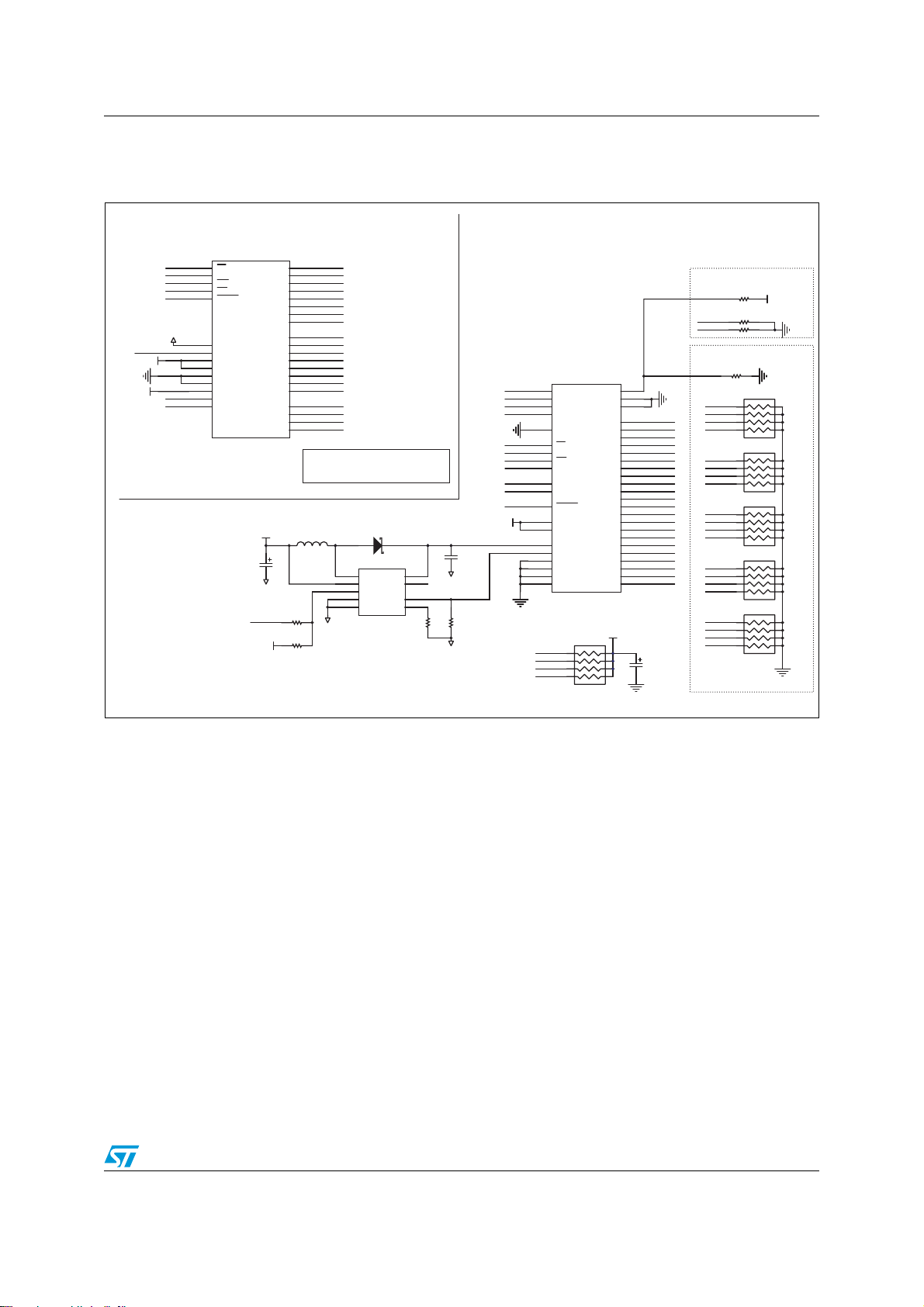
AN3311 Schematics
9.11 LCD 3.2" module with SPI and 16-bit interface 1
Figure 36. LCD 3.2" module with SPI and 16-bit interface 1
CN1
CS
1
RS
2
WR
3
RD
4
#RESET
5
BLGND
SDO
SDI
22
23
24
25
26
27
28
29
30
3.2LCD_connector
BL_Control
VDD
BLVDD
LCD board connector to mother board
CS
RS
WR/SCL
RD
RESET
BL_GND
BL_Control
VDD
VCI
GND
GND
BL_VDD
SDO
SDI
BLVDD
BLGND
BL_Control
BLVDD
PD1
PD2
PD3
PD4
PD5
PD6
PD7
PD8
PD10
PD11
PD12
PD13
PD14
PD15
PD16
PD17
C2
2.2uF
PD1
6
PD2
7
PD3
8
PD4
9
PD5
10
PD6
11
PD7
12
PD8
13
PD10
14
PD11
15
PD12
16
PD13
17
PD14
18
PD15
19
PD16
20
PD17
21
31
XL
XL
32
XR
XR
33
YD
YD
YU
34
YU
The 34-pin connector to mother board for both
serial and 16- bit interface. Compatible with
MB694 with touch screen signals added on
pin 31-34.
4.7uH(1A)
R8
R5
0
do not t
L1
BLGND
U1
8
1
7
9
STLD40DPMR
Z1
STPS1L40M
SW
Vi
EN
GND3FB
PGND
Soldered for i80-system 16-bit interface
R1
10K
VDD
R2
PD16
PD14
PD12
PD10
PD8
PD6
PD4
PD2
PD9
PD0
RS
RD
PD17
PD15
PD13
PD11
PD7
PD5
PD3
PD1
4K7
R3
4K7
R4
0
RP1
10K
RP2
10K
RP3
10K
RP4
10K
RP5
10K
SDO
SDI
Soldered for Serial interface only
CN2
36
VSYNC
HSYNC
DotClk
Enable
CS
WR
RD
RS
SDO
SDI
#RESET
VDD
A
C1
4.7uF/50V
6
Vo
NC
Rset
BLGND
5
4
2
R7
R6
10
100K
BLGND
K
VSYNC
37
HSYNC
38
DOTCLK
39
ENABLE
11
NC
31
CS
34
WR/SCL
35
RD
33
RS
10
SDO
12
SDI
32
RESET
40
VCC
41
VCC
44
LED_A
43
LED_K
6
VSS
42
VSS
45
VSS
1
VSS
FF0245SS1
AM-240320D4TOQW-T00H(R)
RP6
HSYNC
Enable
VSYNC
DotClk
10K
IM0/ID
8
IM1
9
IM3
7
YU
5
YU
YD
XR
XL
D0
D1
D2
D3
D4
D5
D6
D7
D8
D9
D10
D11
D12
D13
D14
D15
D16
D17
VDD
YD
4
XR
3
XL
2
PD0
30
PD1
29
PD2
28
PD3
27
PD4
26
PD5
25
PD6
24
PD7
23
PD8
22
PD9
21
PD10
20
PD11
19
PD12
18
PD13
17
PD14
16
PD15
15
PD16
14
PD17
13
C3
1uF/50V
AM08509v1
Doc ID 18209 Rev 1 55/58

References AN3311
10 References
1. AN3128 application note
2. RM0008 reference manual
3. STM32F10xFWLib 3.2.1 help file
4. STM811 datasheet
5. TN0074 technical note
6. UM0608 user manual
7. STEVAL-IHP001V3 schematics diagram
8. AN2993 application note
9. M24LR64-r datasheet
10. AN2972 application note.
56/58 Doc ID 18209 Rev 1

AN3311 Revision history
11 Revision history
Table 16. Document revision history
Date Revision Changes
14-Dec-2010 1 Initial release.
Doc ID 18209 Rev 1 57/58

AN3311
Please Read Carefully:
Information in this document is provided solely in connection with ST products. STMicroelectronics NV and its subsidiaries (“ST”) reserve the
right to make changes, corrections, modifications or improvements, to this document, and the products and services described herein at any
time, without notice.
All ST products are sold pursuant to ST’s terms and conditions of sale.
Purchasers are solely responsible for the choice, selection and use of the ST products and services described herein, and ST assumes no
liability whatsoever relating to the choice, selection or use of the ST products and services described herein.
No license, express or implied, by estoppel or otherwise, to any intellectual property rights is granted under this document. If any part of this
document refers to any third party products or services it shall not be deemed a license grant by ST for the use of such third party products
or services, or any intellectual property contained therein or considered as a warranty covering the use in any manner whatsoever of such
third party products or services or any intellectual property contained therein.
UNLESS OTHERWISE SET FORTH IN ST’S TERMS AND CONDITIONS OF SALE ST DISCLAIMS ANY EXPRESS OR IMPLIED
WARRANTY WITH RESPECT TO THE USE AND/OR SALE OF ST PRODUCTS INCLUDING WITHOUT LIMITATION IMPLIED
WARRANTIES OF MERCHANTABILITY, FITNESS FOR A PARTICULAR PURPOSE (AND THEIR EQUIVALENTS UNDER THE LAWS
OF ANY JURISDICTION), OR INFRINGEMENT OF ANY PATENT, COPYRIGHT OR OTHER INTELLECTUAL PROPERTY RIGHT.
UNLESS EXPRESSLY APPROVED IN WRITING BY AN AUTHORIZED ST REPRESENTATIVE, ST PRODUCTS ARE NOT
RECOMMENDED, AUTHORIZED OR WARRANTED FOR USE IN MILITARY, AIR CRAFT, SPACE, LIFE SAVING, OR LIFE SUSTAINING
APPLICATIONS, NOR IN PRODUCTS OR SYSTEMS WHERE FAILURE OR MALFUNCTION MAY RESULT IN PERSONAL INJURY,
DEATH, OR SEVERE PROPERTY OR ENVIRONMENTAL DAMAGE. ST PRODUCTS WHICH ARE NOT SPECIFIED AS "AUTOMOTIVE
GRADE" MAY ONLY BE USED IN AUTOMOTIVE APPLICATIONS AT USER’S OWN RISK.
Resale of ST products with provisions different from the statements and/or technical features set forth in this document shall immediately void
any warranty granted by ST for the ST product or service described herein and shall not create or extend in any manner whatsoever, any
liability of ST.
ST and the ST logo are trademarks or registered trademarks of ST in various countries.
Information in this document supersedes and replaces all information previously supplied.
The ST logo is a registered trademark of STMicroelectronics. All other names are the property of their respective owners.
© 2010 STMicroelectronics - All rights reserved
STMicroelectronics group of companies
Australia - Belgium - Brazil - Canada - China - Czech Republic - Finland - France - Germany - Hong Kong - India - Israel - Italy - Japan -
Malaysia - Malta - Morocco - Philippines - Singapore - Spain - Sweden - Switzerland - United Kingdom - United States of America
www.st.com
58/58 Doc ID 18209 Rev 1
 Loading...