


AN2484
Application note
STOTG04 in power down mode
Introduction
A standard USB bus is based on a host-peripheral topology, where the host is typically a PC
which manages the peripherals connected to the bus.
The need to interconnect mobile devices is the purpose for the development of the "OTG
supplement to the USB 2.0 specification" the main target of which is to add host functionality
to devices originally intended as peripherals in USB 2.0.
Battery-powered equipment, such as PDAs and mobile phones, are typical applications for
USB OTG, and therefore for the STOTG04 USB OTG transceiver.
Because increasing battery life is a constant challenge in these products, the STOTG04
implements a power-down operating mode to decrease power consumption. The amount of
current drawn by the transceiver in this mode is dependent on its configuration. This
document is intended to assist in the programming of the STOTG04's internal registers to
achieve minimum power consumption.
April 2007 Rev 1 1/10
www.st.com

Contents AN2484
Contents
1 STOTG04 Description . . . . . . . . . . . . . . . . . . . . . . . . . . . . . . . . . . . . . . . . 3
2 Power-down mode . . . . . . . . . . . . . . . . . . . . . . . . . . . . . . . . . . . . . . . . . . . 4
3 Driver biasing control . . . . . . . . . . . . . . . . . . . . . . . . . . . . . . . . . . . . . . . . 5
4 References . . . . . . . . . . . . . . . . . . . . . . . . . . . . . . . . . . . . . . . . . . . . . . . . . 9
5 Revision history . . . . . . . . . . . . . . . . . . . . . . . . . . . . . . . . . . . . . . . . . . . . 9
2/10
AN2484 STOTG04 Description
1 STOTG04 Description
The STOTG04 is a LS/FS USB OTG transceiver integrating a charge pump for V
generation, an ID line detector and interrupt generator, V
comparators, and integrated
BUS
BUS
voltage
switchable data line pull-up/pull-down resistors. The device is also capable of UART and
Audio Mode operation (refer to AN2148 for more information regarding STOTG04 in an
Audio Carkit Environment).
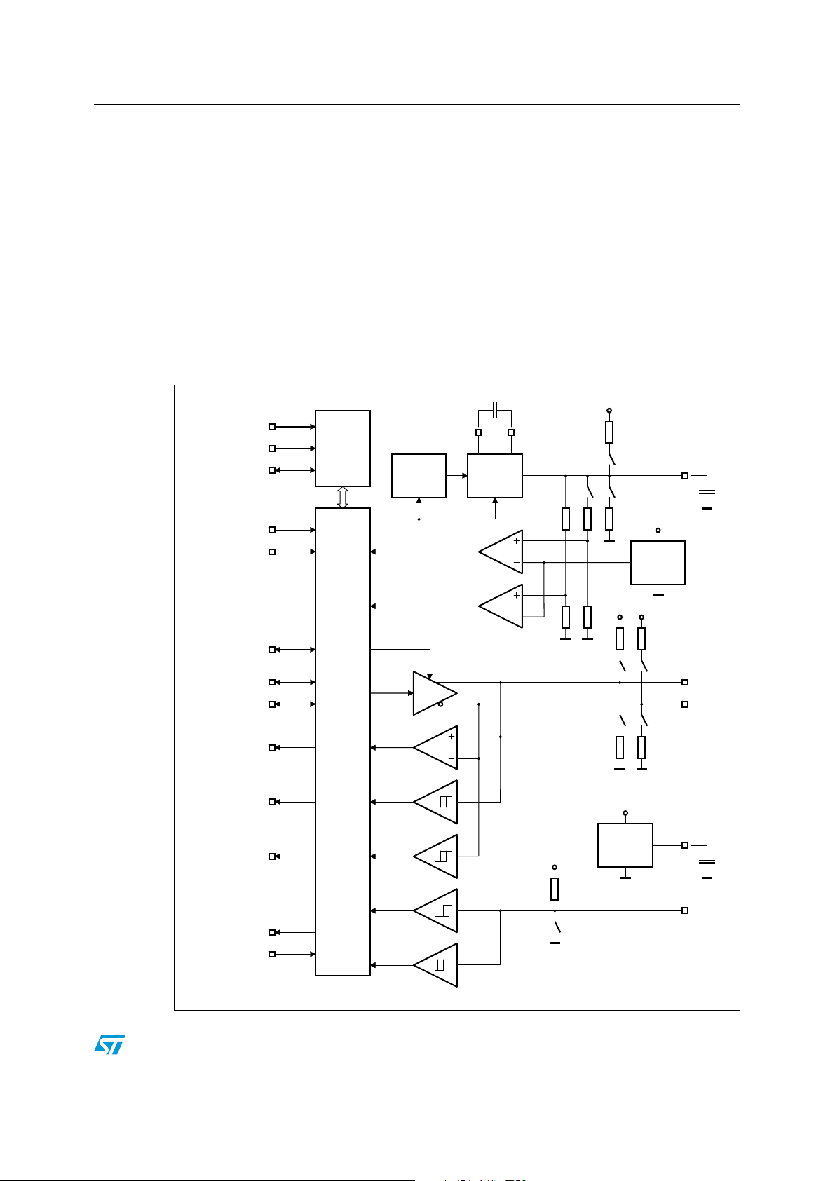
The device can be fully controlled through programming some internal registers through the
2
I
C serial bus. Figure 1 shows a simplified block diagram which can be useful to identify the
internal blocks described in the paragraphs that follow.
Refer to the STOTG04 datasheet for a detailed description of each block.
Figure 1. STOTG04 block diagram
VBAT
ADR_PSW
SCL
SDA
SPEED
SUSPEND
I2C
Interface
Oscillator
Charge
Pump
CAP2CAP1
VBUS
VBAT
Bandgap
Reference
OE_TP_INT/
DAT_VP
SE0_VM
RCV
VP
VM
INT/
RESET/
and
Register Set
Control Logic
VBAT
VTRM
VBAT
Voltage
Regulator
D+
D-
VTRM
ID
3/10

Power-down mode AN2484
2 Power-down mode
The STOTG04 can be placed in power-down mode when there is no need for the USB
function. This mode of operation is controlled by a suspend bit in control register 1, and a
suspend pin. In order to enter power-down mode, both the suspend pin and bit must be set.
This alone, however, is not sufficient to ensure minimum power consumption. Some bits
have higher priority than the suspend bit and could cause some internal blocks to be turned
on even when the STOTG04 is configured in power-down mode. Tab l e 1 contains a detailed
description of the impact on power consumption, in power-down mode, of relevant bits
whose status is not dependent on the suspend bit/pin.
Table 1. Bits having impact on power consumption
Register Bit Bit Name Description
Control 1 6 uart_en
Enables UART mode and turns on regulator
and buffers
Connects DP data line pull up resistor. Pull up
Control 2 0 dp_pull-up
resistors are connected to V
coming from the internal regulator which
therefore has to be on even in suspend mode
when this bit is set
(1)
TRM
Connects DM data line pull up resistor. Pull up
Control 2 1 dm_pull-up
resistors are connected to V
coming from the internal regulator which
TRM
therefore has to be on even in suspend mode
when this bit is set
Shorts the ID pin to ground. This creates a
Control 2 4 id_gnd_drv
Control 2 5 vbus_drv
direct path between V
ID pull-up resistor (which is connected between
and ID)
V
BAT
Turns on internal charge pump even in powerdown mode
and GND through the
BAT
Control 2 7 vbus_chrg Connects a resistor between V
Activates the comparator on DP data line used
Control 3 5 audio_en
for carkit interrupt detection. The comparator
has to be biased leading to increased power
consumption
supply voltage
supply voltage
and V
BUS
BAT
1. If V
voltage is present, the pull-up to V
BUS
internal Voltage Regulator is therefore turned off in order to save current. This does not apply to dm_pullup.
TRM
Ta bl e 2 shows the recommended configuration for minimum power consumption in
power- down mode.
Table 2. Recommended register configuration in power-down mode
Suspend bit Suspend pin Control register 1 Control register 2 Control register 3
1 1 x1x0xx0- 00xx00x0 -xxxx0xx
1. Reserved; x: Don‘t care; Bit order: 0...7
4/10
is disconnected and a 7kΩ pull-up to V
is connected. The
BUS
(1)

AN2484 Driver biasing control
3 Driver biasing control
To reduce power consumption, the STOTG04 allows the user to disable transmitter biasing
in receive mode. This feature is controlled through bit 1 in control register 3 (rec_bias_en).
Although, under normal operating conditions, this function does not affect the transceiver's
performance, laboratory tests have identified some issues when using it in conjunction with
controllers which have shorter than usual output enable-to-data transmission delay.
The problem lies in the time required to properly bias the differential driver, and may cause
compliance test failure.
If data is sent by the controller too early after the output enable signal goes low, the driver's
biasing transient could result in the first bit of the packet not being in line with USB specs.
Lab tests show a longer than expected first bit, which has a significant impact on the eye
pattern and evaluated jitter.
USB compliance software builds the eye diagram using the following algorithm:
once the data packet has been identified, the average data rate and bit time are computed.
Equally spaced (1 bit time) reference points are placed using as a base point the second
crossover of the USB data line. They are then shifted using a least square algorithm to
minimize error between ideal references and actual crossover points. The eye pattern is
then generated, segmenting the waveforms in 1 bit long segments, the limits of which are
the ideal references, and then overlapping each segment.
Figure 1 shows a USB FS data packet where the black points are the references, while the
green ones are actual crossover points.
The longer first bit mentioned above can be easily identified also. This timing error causes
the evaluated average bit rate to be lower than expected, which implies longer average bit
times and therefore higher distances between reference points. The result is a constant shift
in the position of the actual crossover points versus reference points and misalignment in
waveform segments. As a result, the output eye diagram (Figure 3) shows very high
apparent jitter and several mask violations, which lead to compliance test failure.
5/10

Driver biasing control AN2484
Figure 2. USB packet with reference and cross over points
First Bit
Figure 3. Eye pattern with jitter and mask crossing failures
It is worth noting that the sole reason for this failure is the first bit of the data packet, which is
easily demonstrated by removing it from the compliance test. The eye pattern in Figure 4 is
the result.
6/10

AN2484 Driver biasing control
Figure 4. Good eye pattern
Under these circumstances it is recommended to set the bit rec_bias_en in control register
3, making the first bit of the packet fall within specs. This will completely eliminate the eyepattern issues described above.
7/10

Internal control registers AN2484
Appendix A Internal control registers
Table 3. Control register 1
Name Bit R Description
speed 0 1
suspend 1 1
dat_se0 2 0
transp_en 3 0 Enables transparent I
bdis_acon_en 4 0 Enables A-device to connect if B-device disconnect detected
oe_int_en 5 0
uart_en 6 0 Enables UART mode (higher priority than transp_en bit)
7Reserved
– 0 = low-speed mode
– 1 = full-speed mode
– 0 = normal operation
– 1 = power-down mode
– 0 = VP_VM mode
– 1 = DAT_SE0 mode
2
C mode
When set and suspend = 1 then OE_TP_INT/ pin becomes
interrupt output
Table 4. Control register 2
Name Bit R Description
dp_pull-up 0 0 Connects D+ pull-up
dm_pull-up 1 0 Connects D- pull-up
dp_pull-down 2 1 Connects D+ pull-down
dm_pull-down 3 1 Connects D- pull-down
id_gnd_drv 4 0 Connects ID pin to ground
vbus_drv 5 0 Provides power to V
vbus_dischrg 6 0 Discharges V
vbus_chrg 7 0 Charges V
Table 5. Control register 3
Name Bit R Description
00Reserved
rec_bias_en 1 0 Enables transmitter bias even during USB receive
bidi_en 2 1
bdir[0] 3 0
bdir[1] 4 1
8/10
When set, then DAT_VP and SE0_VM pins become bidirectional
otherwise they are inputs only
Direction of the drivers between DAT_VP↔DP and SE0_VM↔DM
in the UART mode
BUS
through a resistor to ground
BUS
through a resistor
BUS

AN2484 References
Table 5. Control register 3 (continued)
Name Bit R Description
audio_en 5 0 Enables car-kit interrupt detector
psw_en 6 0
2V7_en 7 0 Enables 2.7 V voltage regulation instead of 3.3 V
Enables external charge pump control on the ADR_PSW pin.
Disables internal charge pump
Note: R indicates the status of the bit after reset.
4 References
● Universal serial bus specification revision 2.0
● OTG supplement to the USB 2.0 specification
● STOTG04E/ES Datasheet
● AN2148 - STOTG04 in Audio Carkit Environment
5 Revision history
Table 6. Revision history
Date Revision Changes
03-Apr-2007 1 First issue
9/10

AN2484
Please Read Carefully:
Information in this document is provided solely in connection with ST products. STMicroelectronics NV and its subsidiaries (“ST”) reserve the
right to make changes, corrections, modifications or improvements, to this document, and the products and services described herein at any
time, without notice.
All ST products are sold pursuant to ST’s terms and conditions of sale.
Purchasers are solely responsible for the choice, selection and use of the ST products and services described herein, and ST assumes no
liability whatsoever relating to the choice, selection or use of the ST products and services described herein.
No license, express or implied, by estoppel or otherwise, to any intellectual property rights is granted under this document. If any part of this
document refers to any third party products or services it shall not be deemed a license grant by ST for the use of such third party products
or services, or any intellectual property contained therein or considered as a warranty covering the use in any manner whatsoever of such
third party products or services or any intellectual property contained therein.
UNLESS OTHERWISE SET FORTH IN ST’S TERMS AND CONDITIONS OF SALE ST DISCLAIMS ANY EXPRESS OR IMPLIED
WARRANTY WITH RESPECT TO THE USE AND/OR SALE OF ST PRODUCTS INCLUDING WITHOUT LIMITATION IMPLIED
WARRANTIES OF MERCHANTABILITY, FITNESS FOR A PARTICULAR PURPOSE (AND THEIR EQUIVALENTS UNDER THE LAWS
OF ANY JURISDICTION), OR INFRINGEMENT OF ANY PATENT, COPYRIGHT OR OTHER INTELLECTUAL PROPERTY RIGHT.
UNLESS EXPRESSLY APPROVED IN WRITING BY AN AUTHORIZED ST REPRESENTATIVE, ST PRODUCTS ARE NOT
RECOMMENDED, AUTHORIZED OR WARRANTED FOR USE IN MILITARY, AIR CRAFT, SPACE, LIFE SAVING, OR LIFE SUSTAINING
APPLICATIONS, NOR IN PRODUCTS OR SYSTEMS WHERE FAILURE OR MALFUNCTION MAY RESULT IN PERSONAL INJURY,
DEATH, OR SEVERE PROPERTY OR ENVIRONMENTAL DAMAGE. ST PRODUCTS WHICH ARE NOT SPECIFIED AS "AUTOMOTIVE
GRADE" MAY ONLY BE USED IN AUTOMOTIVE APPLICATIONS AT USER’S OWN RISK.
Resale of ST products with provisions different from the statements and/or technical features set forth in this document shall immediately void
any warranty granted by ST for the ST product or service described herein and shall not create or extend in any manner whatsoever, any
liability of ST.
ST and the ST logo are trademarks or registered trademarks of ST in various countries.
Information in this document supersedes and replaces all information previously supplied.
The ST logo is a registered trademark of STMicroelectronics. All other names are the property of their respective owners.
© 2007 STMicroelectronics - All rights reserved
STMicroelectronics group of companies
Australia - Belgium - Brazil - Canada - China - Czech Republic - Finland - France - Germany - Hong Kong - India - Israel - Italy - Japan -
Malaysia - Malta - Morocco - Singapore - Spain - Sweden - Switzerland - United Kingdom - United States of America
www.st.com
10/10
 Loading...